 | –≠–ª–µ–∫—Ç—Ä–æ–Ω–Ω—ã–π –∫–æ–º–ø–æ–Ω–µ–Ω—Ç: ADS8344NB | –°–∫–∞—á–∞—Ç—å:  PDF PDF  ZIP ZIP |

Æ
1
ADS8344
ADS8344
16-Bit, 8-Channel Serial Output Sampling
ANALOG-TO-DIGITAL CONVERTER
FEATURES
q
PIN FOR PIN WITH ADS7844
q
SINGLE SUPPLY: 2.7V to 5V
q
8-CHANNEL SINGLE-ENDED OR
4-CHANNEL DIFFERENTIAL INPUT
q
UP TO 100kHz CONVERSION RATE
q
84dB SINAD
q
SERIAL INTERFACE
q
QSOP-20 AND SSOP-20 PACKAGES
Æ
DESCRIPTION
The ADS8344 is an 8-channel, 16-bit sampling ana-
log-to-digital converter (ADC) with a synchronous
serial interface. Typical power dissipation is 10mW at
a 100kHz throughput rate and a +5V supply. The
reference voltage (V
REF
) can be varied between 500mV
and V
CC
, providing a corresponding input voltage
range of 0V to V
REF
. The device includes a shutdown
mode which reduces power dissipation to under 15
µ
W.
The ADS8344 is guaranteed down to 2.7V operation.
Low power, high speed, and on-board multiplexer
make the ADS8344 ideal for battery operated systems
such as personal digital assistants, portable multi-
channel data loggers, and measurement equipment.
The serial interface also provides low-cost isolation
for remote data acquisition. The ADS8344 is available
in a QSOP-20 or a SSOP-20 package and is guaran-
teed over the ≠40
∞
C to +85
∞
C temperature range.
©
2000 Burr-Brown Corporation
PDS-1571A
Printed in U.S.A. April, 2000
APPLICATIONS
q
DATA ACQUISITION
q
TEST AND MEASUREMENT
q
INDUSTRIAL PROCESS CONTROL
q
PERSONAL DIGITAL ASSISTANTS
q
BATTERY-POWERED SYSTEMS
International Airport Industrial Park ∑ Mailing Address: PO Box 11400, Tucson, AZ 85734 ∑ Street Address: 6730 S. Tucson Blvd., Tucson, AZ 85706 ∑ Tel: (520) 746-1111
Twx: 910-952-1111 ∑ Internet: http://www.burr-brown.com/ ∑ Cable: BBRCORP ∑ Telex: 066-6491 ∑ FAX: (520) 889-1510 ∑ Immediate Product Info: (800) 548-6132
For most current data sheet and other product
information, visit www.burr-brown.com
CDAC
SAR
Comparator
Eight
Channel
Multiplexer
Serial
Interface
and
Control
CH4
CH5
CH6
CH7
COM
V
REF
CS
SHDN
DIN
DOUT
BUSY
DCLK
CH0
CH1
CH2
CH3
§
ADS8344
§
ADS8344

Æ
2
ADS8344
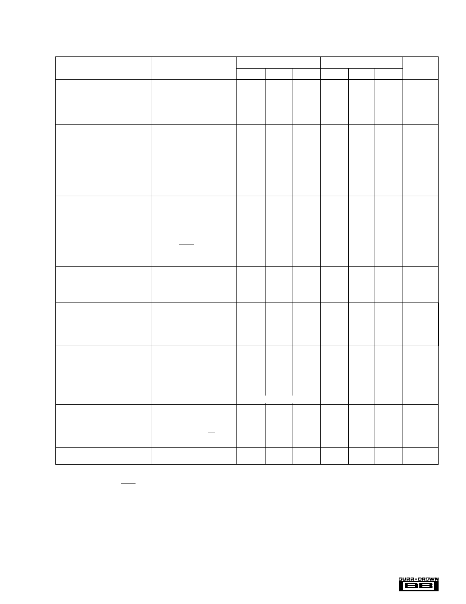
SPECIFICATION: +5V
At T
A
= ≠40
∞
C to +85
∞
C, +V
CC
= +5V, V
REF
= +5V, f
SAMPLE
= 100kHz, and f
CLK
= 24 ∑ f
SAMPLE
= 2.4MHz, unless otherwise noted.
The information provided herein is believed to be reliable; however, BURR-BROWN assumes no responsibility for inaccuracies or omissions. BURR-BROWN assumes
no responsibility for the use of this information, and all use of such information shall be entirely at the user's own risk. Prices and specifications are subject to change
without notice. No patent rights or licenses to any of the circuits described herein are implied or granted to any third party. BURR-BROWN does not authorize or warrant
any BURR-BROWN product for use in life support devices and/or systems.
ADS8344E, N
ADS8344EB, NB
PARAMETER
CONDITIONS
MIN
TYP
MAX
MIN
TYP
MAX
UNITS
ANALOG INPUT
Full-Scale Input Span
Positive Input - Negative Input
0
V
REF
T
T
V
Absolute Input Range
Positive Input
≠0.2
+V
CC
+0.2
T
T
V
Negative Input
≠0.2
+1.25
T
T
V
Capacitance
25
T
pF
Leakage Current
±
1
T
µ
A
SYSTEM PERFORMANCE
Resolution
16
T
Bits
No Missing Codes
14
15
Bits
Integral Linearity Error
8
6
LSB
Offset Error
±
2
±
1
mV
Offset Error Match
1.2
4
T
T
LSB
(1)
Gain Error
±
0.05
±
0.024
%
Gain Error Match
1.0
4
T
T
LSB
Noise
20
T
µ
Vrms
Power Supply Rejection
+4.75V < V
CC
< 5.25V
3
T
LSB
(1)
SAMPLING DYNAMICS
Conversion Time
16
T
Clk Cycles
Acquisition Time
4.5
T
Clk Cycles
Throughput Rate
100
T
kHz
Multiplexer Settling Time
500
T
ns
Aperture Delay
30
T
ns
Aperture Jitter
100
T
ps
Internal Clock Frequency
SHDN = V
DD
2.4
T
MHz
External Clock Frequency
0.024
2.4
T
T
MHz
Data Transfer Only
0
2.4
T
T
MHz
DYNAMIC CHARACTERISTICS
Total Harmonic Distortion
(2)
V
IN
= 5Vp-p at 10kHz
≠90
T
dB
Signal-to-(Noise + Distortion)
V
IN
= 5Vp-p at 10kHz
86
T
dB
Spurious Free Dynamic Range
V
IN
= 5Vp-p at 10kHz
92
T
dB
Channel-to-Channel Isolation
V
IN
= 5Vp-p at 10kHz
100
T
dB
REFERENCE INPUT
Range
0.5
+V
CC
T
T
V
Resistance
DCLK Static
5
T
G
Input Current
40
100
T
T
µ
A
f
SAMPLE
= 12.5kHz
2.5
T
µ
A
DCLK Static
0.001
3
T
T
µ
A
DIGITAL INPUT/OUTPUT
Logic Family
CMOS
T
Logic Levels
V
IH
| I
IH
|
+5
µ
A
3.0
5.5
T
T
V
V
IL
| I
IL
|
+5
µ
A
≠0.3
+0.8
T
T
V
V
OH
I
OH
= ≠250
µ
A
3.5
T
V
V
OL
I
OL
= 250
µ
A
0.4
T
V
Data Format
Straight Binary
T
POWER SUPPLY REQUIREMENTS
+V
CC
Specified Performance
4.75
5.25
T
T
V
Quiescent Current
1.5
2.0
T
mA
f
SAMPLE
= 100kHz
300
T
µ
A
Power-Down Mode
(3)
, CS = +V
CC
3
T
µ
A
Power Dissipation
7.5
10
T
mW
TEMPERATURE RANGE
Specified Performance
≠40
+85
T
T
∞
C
T
Same specifications as ADS8344E.
NOTES: (1) LSB means Least Significant Bit. With V
REF
equal to +5.0V, one LSB is 76
µ
V. (2) First nine harmonics of the test frequency. (3) Auto power-down mode
(PD1 = PD0 = 0) active or SHDN = GND.
Æ
3
ADS8344
SPECIFICATION: +2.7V
At T
A
= ≠40
∞
C to +85
∞
C, +V
CC
= +2.7V, V
REF
= +2.5V, f
SAMPLE
= 100kHz, and f
CLK
= 24 ∑ f
SAMPLE
= 2.4MHz, unless otherwise noted.
ADS8344E, N
ADS8344EB, NB
T
Same specifications as ADS8344E.
NOTES: (1) LSB means Least Significant Bit. With V
REF
equal to +2.5V, one LSB is 38
µ
V. (2) First nine harmonics of the test frequency. (3) Auto power-down mode
(PD1 = PD0 = 0) active or SHDN = GND.
PARAMETER
CONDITIONS
MIN
TYP
MAX
MIN
TYP
MAX
UNITS
ANALOG INPUT
Full-Scale Input Span
Positive Input - Negative Input
0
V
REF
T
T
V
Absolute Input Range
Positive Input
≠0.2
+V
CC
+0.2
T
T
V
Negative Input
≠0.2
+0.2
T
T
V
Capacitance
25
T
pF
Leakage Current
±
1
T
µ
A
SYSTEM PERFORMANCE
Resolution
16
T
Bits
No Missing Codes
14
15
Bits
Integral Linearity Error
12
8
LSB
Offset Error
±
1
0.5
mV
Offset Error Match
1.2
4
T
T
LSB
Gain Error
±
0.05
±
0.0024
% of FSR
Gain Error Match
1
4
T
T
LSB
Noise
20
T
µ
Vrms
Power Supply Rejection
+2.7 < V
CC
< +3.3V
3
T
LSB
(1)
SAMPLING DYNAMICS
Conversion Time
16
T
Clk Cycles
Acquisition Time
4.5
T
Clk Cycles
Throughput Rate
100
T
kHz
Multiplexer Settling Time
500
T
ns
Aperture Delay
30
T
ns
Aperture Jitter
100
T
ps
Internal Clock Frequency
SHDN = V
DD
2.4
T
MHz
External Clock Frequency
0.024
2.0
T
T
MHz
Data Transfer Only
0
2.0
T
T
MHz
DYNAMIC CHARACTERISTICS
Total Harmonic Distortion
(2)
V
IN
= 2.5Vp-p at 1kHz
≠90
T
dB
Signal-to-(Noise + Distortion)
V
IN
= 2.5Vp-p at 1kHz
86
T
dB
Spurious Free Dynamic Range
V
IN
= 2.5Vp-p at 1kHz
92
T
dB
Channel-to-Channel Isolation
V
IN
= 2.5Vp-p at 10kHz
100
T
dB
REFERENCE INPUT
Range
0.5
+V
CC
T
T
V
Resistance
DCLK Static
5
T
G
Input Current
13
40
T
T
µ
A
f
SAMPLE
= 12.5kHz
2.5
T
µ
A
DCLK Static
0.001
3
T
T
µ
A
DIGITAL INPUT/OUTPUT
Logic Family
CMOS
T
Logic Levels
V
IH
| I
IH
|
+5
µ
A
+V
CC
∑ 0.7
5.5
T
T
V
V
IL
| I
IL
|
+5
µ
A
≠0.3
+0.8
T
T
V
V
OH
I
OH
= ≠250
µ
A
+V
CC
∑ 0.8
T
V
V
OL
I
OL
= 250
µ
A
0.4
T
V
Data Format
Straight Binary
T
POWER SUPPLY REQUIREMENTS
+V
CC
Specified Performance
2.7
3.6
T
T
V
Quiescent Current
1.2
1.85
T
T
mA
f
SAMPLE
= 100kHz
220
T
µ
A
Power-Down Mode
(3)
, CS = +V
CC
3
T
µ
A
Power Dissipation
3.2
5
T
mW
TEMPERATURE RANGE
Specified Performance
≠40
+85
T
T
∞
C

Æ
4
ADS8344
PIN CONFIGURATION
Top View
PIN DESCRIPTIONS
PIN
NAME
DESCRIPTION
1
CH0
Analog Input Channel 0.
2
CH1
Analog Input Channel 1.
3
CH2
Analog Input Channel 2.
4
CH3
Analog Input Channel 3.
5
CH4
Analog Input Channel 4.
6
CH5
Analog Input Channel 5.
7
CH6
Analog Input Channel 6.
8
CH7
Analog Input Channel 7.
9
COM
Ground reference for analog inputs. Sets zero code
voltage in single ended mode. Connect this pin to ground
or ground reference point.
10
SHDN
Shutdown. When LOW, the device enters a very low
power shutdown mode.
11
V
REF
Voltage Reference Input. See Specification Table for
ranges.
12
+V
CC
Power Supply, 2.7V to 5V.
13
GND
Ground
14
GND
Ground
15
D
OUT
Serial Data Output. Data is shifted on the falling edge of
D
CLK
. This output is high impedance when
CS is high.
16
BUSY
Busy Output. Busy goes low when the DIN control bits
are being read and also when the device is converting.
The Output is high impedance when CS is High.
17
D
IN
Serial Data Input. If CS is LOW, data is latched on rising
edge of D
CLK
.
18
CS
Chip Select Input. Active LOW. Data will not be clocked
into D
IN
unless CS is low. When CS is high D
OUT
is high
impedance.
19
CLK
External Clock Input. The clock speed determines the
conversion rate by the equation f
CLK
= 24 ∑ f
SAMPLE
.
20
+V
CC
Power Supply
MINIMUM
RELATIVE
MAXIMUM
SPECIFICATION
PACKAGE
ACCURACY
GAIN ERROR
TEMPERATURE
DRAWING
ORDERING
TRANSPORT
PRODUCT
(LSB)
(%)
RANGE
PACKAGE
NUMBER
NUMBER
(1)
MEDIA
ADS8344E
8
±
0.05
≠40
∞
C to +85
∞
C
QSOP-20
349
ADS8344E
Rails
"
"
"
"
"
"
ADS8344E/2K5
Tape and Reel
ADS8344N
"
"
"
SSOP-20
334
ADS8344N
Rails
"
"
"
"
"
"
ADS8344N/1K
Tape and Reel
ADS8344EB
6
±
0.024
≠40
∞
C to +85
∞
C
QSOP-20
349
ADS8344EB
Rails
"
"
"
"
"
"
ADS8344EB/2K5
Tape and Reel
ADS8344NB
"
"
"
SSOP-20
334
ADS8344NB
Rails
"
"
"
"
"
"
ADS8344NB/1K
Tape and Reel
NOTES: (1) Models with a slash (/) are available only in Tape and Reel in the quantities indicated (e.g., /2K5 indicates 2500 devices per reel). Ordering 2500 pieces
of "ADS8344E/2K5" will get a single 2500-piece Tape and Reel.
PACKAGE/ORDERING INFORMATION
ABSOLUTE MAXIMUM RATINGS
(1)
+V
CC
to GND ........................................................................ ≠0.3V to +6V
Analog Inputs to GND ............................................ ≠0.3V to +V
CC
+ 0.3V
Digital Inputs to GND ........................................................... ≠0.3V to +6V
Power Dissipation .......................................................................... 250mW
Maximum Junction Temperature ................................................... +150
∞
C
Operating Temperature Range ........................................ ≠40
∞
C to +85
∞
C
Storage Temperature Range ......................................... ≠65
∞
C to +150
∞
C
Lead Temperature (soldering, 10s) ............................................... +300
∞
C
NOTE: (1) Stresses above those listed under "Absolute Maximum Ratings"
may cause permanent damage to the device. Exposure to absolute maximum
conditions for extended periods may affect device reliability.
ELECTROSTATIC
DISCHARGE SENSITIVITY
This integrated circuit can be damaged by ESD. Burr-Brown
recommends that all integrated circuits be handled with
appropriate precautions. Failure to observe proper handling and
installation procedures can cause damage.
ESD damage can range from subtle performance degradation to
complete device failure. Precision integrated circuits may be
more susceptible to damage because very small parametric
changes could cause the device not to meet its published specifi-
cations.
1
2
3
4
5
6
7
8
9
10
CH0
CH1
CH2
CH3
CH4
CH5
CH6
CH7
COM
SHDN
+V
CC
D
CLK
CS
D
IN
BUSY
D
OUT
GND
GND
+V
CC
V
REF
20
19
18
17
16
15
14
13
12
11
ADS8344

Æ
5
ADS8344
TYPICAL PERFORMANCE CURVES: +5V
At T
A
= +25
∞
C, +V
CC
= +5V, V
REF
= +5V, f
SAMPLE
= 100kHz, and f
CLK
= 24 ∑ f
SAMPLE
= 2.4MHz, unless otherwise noted.
0
≠20
≠40
≠60
≠80
≠100
≠120
≠140
≠160
FREQUENCY SPECTRUM
(4096 Point FFT; f
IN
= 1.001kHz, ≠0.2dB)
0
10
20
30
40
50
Frequency (kHz)
Amplitude (dB)
0
≠20
≠40
≠60
≠80
≠100
≠120
≠140
≠160
FREQUENCY SPECTRUM
(4096 Point FFT; f
IN
= 9.985kHz, ≠0.2dB)
0
10
20
30
40
50
Frequency (kHz)
Amplitude (dB)
SIGNAL-TO-NOISE RATIO AND SIGNAL-TO-
(NOISE+DISTORTION) vs INPUT FREQUENCY
10
1
100
Frequency (kHz)
SNR and SINAD (dB)
100
90
80
70
60
SINAD
SNR
SPURIOUS FREE DYNAMIC RANGE AND TOTAL
HARMONIC DISTORTION vs INPUT FREQUENCY
10
1
100
Frequency (kHz)
SFDR (dB)
THD (dB)
100
90
80
70
60
≠100
≠90
≠80
≠70
≠60
THD
(1)
SFDR
NOTE: (1) First Nine Harmonics
of the Input Frequency
CHANGE IN SIGNAL-TO-(NOISE+DISTORTION)
vs TEMPERATURE
≠40
≠25
0
20
50
75
100
Temperature (∞C)
Delta from +25
∞
C (dB)
0.2
0.0
≠0.2
≠0.4
≠0.6
≠0.8
0.4
f
IN
= 9.985kHz, ≠0.2dB
EFFECTIVE NUMBER OF BITS
vs INPUT FREQUENCY
10
1
100
Frequency (kHz)
Effective Number of Bits
15.0
14.5
14.0
13.5
13.0
12.5
12.0
11.5
11.0

Æ
6
ADS8344
TYPICAL PERFORMANCE CURVES: +2.7V
At T
A
= +25
∞
C, +V
CC
= +2.7V, V
REF
= +2.5V, f
SAMPLE
= 100kHz, and f
CLK
= 24 ∑ f
SAMPLE
= 2.4MHz, unless otherwise noted.
TYPICAL PERFORMANCE CURVES: +5V
(Cont.)
At T
A
= +25
∞
C, +V
CC
= +5V, V
REF
= +5V, f
SAMPLE
= 100kHz, and f
CLK
= 24 ∑ f
SAMPLE
= 2.4MHz, unless otherwise noted.
Output Code
2
1
0
≠1
≠2
≠3
≠4
INTEGRAL LINEARITY ERROR vs CODE
8000
H
C000
H
FFFF
H
0000
H
4000
H
ILE (LSB)
Output Code
3
2
1
0
≠1
≠2
≠3
DIFFERENTIAL LINEARITY ERROR vs CODE
8000
H
C000
H
FFFF
H
0000
H
4000
H
DLE (LSB)
0
≠20
≠40
≠60
≠80
≠100
≠120
≠140
≠160
FREQUENCY SPECTRUM
(4096 Point FFT; f
IN
= 1.001kHz, ≠0.2dB)
0
10
20
30
40
50
Frequency (kHz)
Amplitude (dB)
0
≠20
≠40
≠60
≠80
≠100
≠120
≠140
≠160
FREQUENCY SPECTRUM
(4096 Point FFT; f
IN
= 9.985kHz, ≠0.2dB)
0
10
20
30
40
50
Frequency (kHz)
Amplitude (dB)
SIGNAL-TO-NOISE RATIO AND SIGNAL-TO-
(NOISE+DISTORTION) vs INPUT FREQUENCY
10
1
100
Frequency (kHz)
SNR and SINAD (dB)
100
90
80
70
60
50
SINAD
SNR
SPURIOUS FREE DYNAMIC RANGE AND TOTAL
HARMONIC DISTORTION vs INPUT FREQUENCY
10
1
100
Frequency (kHz)
SFDR (dB)
THD
(1)
SFDR
100
90
80
70
60
50
THD (dB)
≠100
≠90
≠80
≠70
≠60
≠50
NOTE: (1) First Nine Harmonics
of the Input Frequency

Æ
7
ADS8344
EFFECTIVE NUMBER OF BITS
vs INPUT FREQUENCY
10
1
100
Frequency (kHz)
Effective Number of Bits
15
14
13
12
11
10
9
8
CHANGE IN SIGNAL-TO-(NOISE+DISTORTION)
vs TEMPERATURE
≠40
≠25
0
20
50
75
100
Temperature (∞C)
Delta from +25
∞
C (dB)
2.0
1.5
1.0
0.5
0.0
≠0.5
≠1.0
≠1.5
≠2.0
f
IN
= 9.985kHz, ≠0.2dB
TYPICAL PERFORMANCE CURVES: +2.7V
(Cont.)
At T
A
= +25
∞
C, +V
CC
= +2.7V, V
REF
= +2.5V, f
SAMPLE
= 100kHz, and f
CLK
= 24 ∑ f
SAMPLE
= 2.4MHz, unless otherwise noted.
Output Code
3
2
1
0
≠1
≠2
≠3
INTEGRAL LINEARITY ERROR vs CODE
8000
H
C000
H
FFFF
H
0000
H
4000
H
ILE (LSB)
Output Code
3
2
1
0
≠1
≠2
≠3
DIFFERENTIAL LINEARITY ERROR vs CODE
8000
H
C000
H
FFFF
H
0000
H
4000
H
DLE (LSB)
SUPPLY CURRENT vs +V
SS
2.5
3.0
3.5
4.0
4.5
5.0
+V
SS
(V)
Supply Current (mA)
1.6
1.5
1.4
1.3
1.2
1.1
1.0
f
SAMPLE
= 100kHz, V
REF
= +V
SS

Æ
8
ADS8344
THEORY OF OPERATION
The ADS8344 is a classic successive approximation register
(SAR) analog-to-digital (A/D) converter. The architecture is
based on capacitive redistribution which inherently includes
a sample/hold function. The converter is fabricated on a
0.6
µ
s CMOS process.
The basic operation of the ADS8344 is shown in Figure 1.
The device requires an external reference and an external
clock. It operates from a single supply of 2.7V to 5.25V. The
external reference can be any voltage between 500mV and
+V
CC
. The value of the reference voltage directly sets the
input range of the converter. The average reference input
current depends on the conversion rate of the ADS8344.
The analog input to the converter is differential and is
provided via an eight-channel multiplexer. The input can be
provided in reference to a voltage on the COM pin (which
is generally ground) or differentially by using four of the
eight input channels (CH0 - CH7). The particular configura-
tion is selectable via the digital interface.
A2
A1
A0
CH0
CH1
CH2
CH3
CH4
CH5
CH6
CH7
0
0
0
+IN
≠IN
0
0
1
+IN
≠IN
0
1
0
+IN
≠IN
0
1
1
+IN
≠IN
1
0
0
≠IN
+IN
1
0
1
≠IN
+IN
1
1
0
≠IN
+IN
1
1
1
≠IN
+IN
TABLE II. Differential Channel Control (SGL/DIF LOW).
TABLE I. Single-Ended Channel Selection (SGL/DIF HIGH).
FIGURE 1. Basic Operation of the ADS8344.
A2
A1
A0
CH0
CH1
CH2
CH3
CH4
CH5
CH6
CH7
COM
0
0
0
+IN
≠IN
1
0
0
+IN
≠IN
0
0
1
+IN
≠IN
1
0
1
+IN
≠IN
0
1
0
+IN
≠IN
1
1
0
+IN
≠IN
0
1
1
+IN
≠IN
1
1
1
+IN
≠IN
ANALOG INPUT
Figure 2 shows a block diagram of the input multiplexer on
the ADS8344. The differential input of the converter is
derived from one of the eight inputs in reference to the COM
pin or four of the eight inputs. Table I and Table II show the
relationship between the A2, A1, A0, and SGL/DIF control
bits and the configuration of the analog multiplexer. The
control bits are provided serially via the DIN pin, see the
Digital Interface section of this data sheet for more details.
When the converter enters the hold mode, the voltage
difference between the +IN and ≠IN inputs (see Figure 2) is
captured on the internal capacitor array. The voltage on the
≠IN input is limited between ≠0.2V and 1.25V, allowing the
input to reject small signals which are common to both the
+IN and ≠IN input. The +IN input has a range of ≠0.2V to
+V
CC
+ 0.2V.
The input current on the analog inputs depends on the
conversion rate of the device. During the sample period, the
source must charge the internal sampling capacitor (typi-
CH0
CH1
CH2
CH3
CH4
CH5
CH6
CH7
COM
SHDN
1
2
3
4
5
6
7
8
9
10
20
19
18
17
16
15
14
13
12
11
+V
CC
D
CLK
CS
D
IN
BUSY
D
OUT
GND
GND
+V
CC
V
REF
Serial/Conversion Clock
Chip Select
Serial Data In
Serial Data Out
+2.7V to +5V
1
µ
F to 10
µ
F
ADS8344
Single-ended
or differential
analog inputs
1
µ
F to 10
µ
F
0.1
µ
F

Æ
9
ADS8344
cally 25pF). After the capacitor has been fully charged, there
is no further input current. The rate of charge transfer from
the analog source to the converter is a function of conversion
rate.
REFERENCE INPUT
The external reference sets the analog input range. The
ADS8344 will operate with a reference in the range of
100mV to +V
CC
. Keep in mind that the analog input is the
difference between the +IN input and the ≠IN input as shown
in Figure 2. For example, in the single-ended mode, a 1.25V
reference, and with the COM pin grounded, the selected input
channel (CH0 - CH7) will properly digitize a signal in the
range of 0V to 1.25V. If the COM pin is connected to 0.5V,
the input range on the selected channel is 0.5V to 1.75V.
There are several critical items concerning the reference input
and its wide voltage range. As the reference voltage is re-
duced, the analog voltage weight of each digital output code
is also reduced. This is often referred to as the LSB (least
significant bit) size and is equal to the reference voltage
divided by 65536. Any offset or gain error inherent in the
A/D converter will appear to increase, in terms of LSB size,
as the reference voltage is reduced. For example, if the offset
of a given converter is 2 LSBs with a 2.5V reference, then it
will typically be 10 LSBs with a 0.5V reference. In each case,
the actual offset of the device is the same, 76.3
µ
V.
FIGURE 2. Simplified Diagram of the Analog Input.
Converter
+IN
≠IN
CH0
CH1
CH2
CH3
A2-A0
(shown 00o
B
)
(1)
SGL/DIF
(shown HIGH)
CH4
CH5
CH6
CH7
COM
NOTE: (1) See Truth Tables, Table I
and Table II for address coding.
Likewise, the noise or uncertainty of the digitized output will
increase with lower LSB size. With a reference voltage of
500mV, the LSB size is 7.6
µ
V. This level is below the
internal noise of the device. As a result, the digital output
code will not be stable and vary around a mean value by a
number of LSBs. The distribution of output codes will be
gaussian and the noise can be reduced by simply averaging
consecutive conversion results or applying a digital filter.
With a lower reference voltage, care should be taken to
provide a clean layout including adequate bypassing, a clean
(low noise, low ripple) power supply, a low-noise reference,
and a low-noise input signal. Because the LSB size is lower,
the converter will also be more sensitive to nearby digital
signals and electromagnetic interference.
The voltage into the V
REF
input is not buffered and directly
drives the capacitor digital-to-analog converter (CDAC)
portion of the ADS8344. Typically, the input current is
13
µ
A with a 2.5V reference. This value will vary by
microamps depending on the result of the conversion. The
reference current diminishes directly with both conversion
rate and reference voltage. As the current from the reference
is drawn on each bit decision, clocking the converter more
quickly during a given conversion period will not reduce
overall current drain from the reference.
DIGITAL INTERFACE
The ADS8344 has a four-wire serial interface compatible
with several microprocessor families (note that the digital
inputs are over-voltage tolerant up to +5.5V, regardless of
+V
CC
). Figure 3 shows the typical operation of the ADS8344
digital interface.
Most microprocessors communicate using 8-bit transfers;
the ADS8344 can complete a conversion with three such
transfers, for a total of 24 clock cycles on the DCLK input,
provided the timing is as shown in Figure 3.
The first eight clock cycles are used to provide the control
byte via the DIN pin. When the converter has enough
information about the following conversion to set the input
multiplexer appropriately, it enters the acquisition (sample)
mode. After four more clock cycles, the control byte is
complete and the converter enters the conversion mode. At
this point, the input sample/hold goes into the hold mode.
The next sixteen clock cycles accomplish the actual A/D
conversion.
Control Byte
Also, shown in Figure 3 is the placement and order of the
control bits within the control byte. Table III and IV give
detailed information about these bits. The first bit, the "S"
bit, must always be HIGH and indicates the start of the
control byte. The ADS8344 will ignore inputs on the DIN
pin until the start bit is detected. The next three bits (A2-A0)
select the active input channel or channels of the input
multiplexer (see Tables I and II and Figure 2).
The SGL/DIF-bit controls the multiplexer input mode: ei-
ther single-ended mode, the selected input channel is refer-
enced to the COM pin. In differential mode, the two selected

Æ
10
ADS8344
inputs provide a differential input. See Tables I and II and
Figure 2 for more information. The last two bits (PD1 - PD0)
select the power-down mode and clock mode as shown in
Table V. If both PD1 and PD0 are HIGH, the device is
always powered up. If both PD1 and PD0 are low, the device
enters a power-down mode between conversions. When a
new conversion is initiated, the device will resume normal
operation instantly--no delay is needed to allow the device
to power up and the very first conversion will be valid.
Clock Modes
The ADS8344 can be used with an external serial clock or
an internal clock to perform the successive-approximation
conversion. In both clock modes, the external clock shifts
data in and out of the device. Internal clock mode is selected
when PD1 is HIGH and PD0 is LOW.
External Clock Mode
In external clock mode, the external clock not only shifts
data in and out of the ADS8344, it also controls the A/D
conversion steps. BUSY will go HIGH for one clock period
after the last bit of the control byte is shifted in. Successive-
approximation bit decisions are made and appear at DOUT
on each of the next 16 SCLK falling edges (Figure 3). Figure
4 shows the BUSY timing in external clock mode.
FIGURE 3. Conversion Timing, 24-Clocks per Conversion, 8-Bit Bus Interface. No DCLK delay required with dedicated
serial port.
t
ACQ
Acquire
Idle
Conversion
1
DCLK
CS
8
1
15
DOUT
BUSY
(MSB)
(START)
(LSB)
A2
S
DIN
A1
A0
SGL/
DIF
PD1 PD0
14
13
12
11
10
9
8
7
6
5
4
3
2
1
0
Zero Filled...
8
1
8
Acquire
Idle
Conversion
1
8
1
15
(MSB)
(START)
A2
S
A1
A0
SGL/
DIF
PD1 PD0
14
Bit 7
Bit 6
Bit 5
Bit 4
Bit 3
Bit 2
Bit 1
Bit 0
(MSB)
(LSB)
S
A2
A1
A0
--
SGL/DIF
PD1
PD0
TABLE III. Order of the Control Bits in the Control Byte.
TABLE IV. Descriptions of the Control Bits within the
Control Byte.
BIT
NAME
DESCRIPTION
7
S
Start Bit. Control byte starts with first HIGH bit on
DIN.
6 - 4
A2 - A0
Channel Select Bits. Along with the SGL/DIF bit,
these bits control the setting of the multiplexer input
as detailed in Tables I and II.
2
SGL/DIF
Single-Ended/Differential Select Bit. Along with bits
A2 - A0, this bit controls the setting of the multiplexer
input as detailed in Tables I and II.
1 - 0
PD1 - PD0
Power-Down Mode Select Bits. See Table V for
details.
PD0
PD1
Description
0
0
Power-down between conversions. When each
conversion is finished, the converter enters a low
power mode. At the start of the next conversion,
the device instantly powers up to full power. There
is no need for additional delays to assure full
operation and the very first conversion is valid.
0
1
Internal clock mode.
1
0
Reserved for future use.
1
1
No power-down between conversions, device al-
ways powered.
TABLE V. Power-Down Selection.
FIGURE 4. Detailed Timing Diagram.
PD0
t
BDV
t
DH
t
CH
t
CL
t
DS
t
CSS
t
DV
t
BD
t
BD
t
TR
t
BTR
t
D0
t
CSH
DCLK
CS
15
DOUT
BUSY
DIN
14

Æ
11
ADS8344
SYMBOL
DESCRIPTION
MIN
TYP
MAX
UNITS
t
ACQ
Acquisition Time
1.5
µ
s
t
DS
DIN Valid Prior to DCLK Rising
100
ns
t
DH
DIN Hold After DCLK HIGH
10
ns
t
DO
DCLK Falling to DOUT Valid
200
ns
t
DV
CS Falling to DOUT Enabled
200
ns
t
TR
CS Rising to DOUT Disabled
200
ns
t
CSS
CS Falling to First DCLK Rising
100
ns
t
CSH
CS Rising to DCLK Ignored
0
ns
t
CH
DCLK HIGH
200
ns
t
CL
DCLK LOW
200
ns
t
BD
DCLK Falling to BUSY Rising
200
ns
t
BDV
CS Falling to BUSY Enabled
200
ns
t
BTR
CS Rising to BUSY Disabled
200
ns
TABLE VI. Timing Specifications (+V
CC
= +2.7V to 3.6V,
T
A
= ≠40
∞
C to +85
∞
C, C
LOAD
= 50pF).
Since one clock cycle of the serial clock is consumed with
BUSY going high (while the MSB decision is being made),
16 additional clocks must be given to clock out all 16 bits of
data; thus, one conversion takes a minimum of 25 clock
cycles to fully read the data. Since most microprocessors
communicate in 8-bit transfers, this means that an additional
transfer must be made to capture the LSB.
There are two ways of handling this requirement. One is
shown in Figure 3, where the beginning of the next control
byte appears at the same time the LSB is being clocked out
of the ADS8344. This method allows for maximum through-
put and 24 clock cycles per conversion.
The other method is shown in Figure 5, which uses 32 clock
cycles per conversion; the last seven clock cycles simply
shift out zeros on the DOUT line. BUSY and DOUT go into
a high-impedance state when CS goes high; after the next CS
falling edge, BUSY will go LOW.
Internal Clock Mode
In internal clock mode, the ADS8344 generates its own
conversion clock internally. This relieves the microproces-
sor from having to generate the SAR conversion clock and
allows the conversion result to be read back at the processor's
convenience, at any clock rate up to 2.4MHz. BUSY goes
HIGH at the start of conversion and then returns LOW when
the conversion is complete. During the conversion, BUSY
will remain LOW for a maximum of 8
µ
s. Also, during the
conversion, SCLK should remain LOW to achieve the best
noise performance. The conversion result is stored in an
internal register; the data may be clocked out of this register
any time after the conversion is complete.
t
ACQ
Acquire
Idle
Conversion
1
DCLK
CS
8
1
15
DOUT
BUSY
(MSB)
(START)
(LSB)
A2
S
DIN
A1
A0
SGL/
DIF
PD1 PD0
14
13
12
11
10
9
8
7
6
5
4
3
2
1
0
8
1
8
Idle
1
8
Zero Filled...
If CS is LOW when BUSY goes LOW following a conver-
sion, the next falling edge of the external serial clock will
write out the MSB on the DOUT line. The remaining bits
(D14-D0) will be clocked out on each successive clock cycle
following the MSB. If CS is HIGH when BUSY goes LOW
then the DOUT line will remain in tri-state until CS goes
LOW (Figure 6). CS does not need to remain LOW once a
conversion has started. Note that BUSY is not tri-stated
when CS goes HIGH in internal clock mode.
Data can be shifted in and out of the ADS8344 at clock rates
exceeding 2.4MHz, provided that the minimum acquisition
time t
ACQ
, is kept above 1.7
µ
s.
Digital Timing
Figure 4 and Tables VI and VII provide detailed timing for
the digital interface of the ADS8344.
t
ACQ
Acquire
Idle
Conversion
1
DCLK
CS
8
9
10
11
12
13
14
15
16
17
18
19
20
21
22
23
24
25
26
27
28
29
30
31
32
15
DOUT
BUSY
(MSB)
(START)
(LSB)
A2
S
DIN
A1
A0
SGL/
DIF
PD1 PD0
14
13
12
11
10
9
8
7
6
5
4
3
2
1
0
Zero Filled...
FIGURE 5.
FIGURE 6.

Æ
12
ADS8344
SYMBOL
DESCRIPTION
MIN
TYP
MAX
UNITS
t
ACQ
Acquisition Time
1.7
µ
s
t
DS
DIN Valid Prior to DCLK Rising
50
ns
t
DH
DIN Hold After DCLK HIGH
10
ns
t
DO
DCLK Falling to DOUT Valid
100
ns
t
DV
CS Falling to DOUT Enabled
70
ns
t
TR
CS Rising to DOUT Disabled
70
ns
t
CSS
CS Falling to First DCLK Rising
50
ns
t
CSH
CS Rising to DCLK Ignored
0
ns
t
CH
DCLK HIGH
150
ns
t
CL
DCLK LOW
150
ns
t
BD
DCLK Falling to BUSY Rising
100
ns
t
BDV
CS Falling to BUSY Enabled
70
ns
t
BTR
CS Rising to BUSY Disabled
70
ns
FIGURE 7. Ideal Input Voltages and Output Codes.
TABLE VII. Timing Specifications (+V
CC
= +4.75V to
+5.25V, T
A
= ≠40
∞
C to +85
∞
C, C
LOAD
= 50pF).
Output Code
0V
FS = Full-Scale Voltage = V
REF
1 LSB = V
REF
/65,536
FS ≠ 1 LSB
11...111
11...110
11...101
00...010
00...001
00...000
1 LSB
NOTE
(1)
: Voltage at converter input, after
multiplexer: +IN≠(≠IN). (See Figure 2.)
Input Voltage
(1)
(V)
Data Format
The ADS8344 output data is in straight binary format as
shown in Figure 7. This figure shows the ideal output code
for the given input voltage and does not include the effects
of offset, gain, or noise.
POWER DISSIPATION
There are three power modes for the ADS8344: full power
(PD1 - PD0 = 11B), auto power-down (PD1 - PD0 = 00B),
and shutdown (SHDN LOW). The effects of these modes
varies depending on how the ADS8344 is being operated.
For example, at full conversion rate and 24-clocks per
conversion, there is very little difference between full power
mode and auto power-down, a shutdown (SHDN LOW) will
not lower power dissipation
When operating at full-speed and 24-clocks per conversion
(as shown in Figure 3), the ADS8344 spends most of its time
acquiring or converting. There is little time for auto power-
down, assuming that this mode is active. Thus, the differ-
ence between full power mode and auto power-down is
negligible. If the conversion rate is decreased by simply
slowing the frequency of the DCLK input, the two modes
remain approximately equal. However, if the DCLK fre-
quency is kept at the maximum rate during a conversion, but
conversions are simply done less often, then the difference
between the two modes is dramatic. In the latter case, the
converter spends an increasing percentage of its time in
power-down mode (assuming the auto power-down mode is
active).
If DCLK is active and CS is LOW while the ADS8344 is in
auto power-down mode, the device will continue to dissipate
some power in the digital logic. The power can be reduced
to a minimum by keeping CS HIGH.
Operating the ADS8344 in auto power-down mode will
result in the lowest power dissipation, and there is no
conversion time "penalty" on power-up. The very first
conversion will be valid. SHDN can be used to force an
immediate power-down.
NOISE
The noise floor of the ADS8344 itself is extremely low, as
can be seen from Figures 8 thru 11, and is much lower than
competing A/D converters. The ADS8344 was tested at both
5V and 2.7V and in both the internal and external clock
modes. A low level DC input was applied to the analog input
pins and the converter was put through 5,000 conversions.
The digital output of the A/D converter will vary in output
code due to the internal noise of the ADS8344. This is true
for all 16-bit SAR-type A/D converters. Using a histogram
to plot the output codes, the distribution should appear bell-
shaped with the peak of the bell curve representing the
nominal code for the input value. The
±
1
,
±
2
, and
±
3
distributions will represent the 68.3%, 95.5%, and 99.7%,
respectively, of all codes. The transition noise can be calcu-
lated by dividing the number of codes measured by 6 and
this will yield the
±
3
distribution or 99.7% of all codes.
Statistically, up to 3 codes could fall outside the distribution
when executing 1000 conversions. The ADS8344, with < 3
output codes for the
±
3
distribution, will yield a <
±
0.5LSB
transition noise at 5V operation. Remember, to achieve this
low noise performance, the peak-to-peak noise of the input
signal and reference must be < 50
µ
V.
FIGURE 8. Histogram of 5000 Conversions of a DC Input at the
Code Transition, 5V operation external clock mode.
Code
4561
242
0
0
197
7FFE
7FFD
8001
8000
7FFF

Æ
13
ADS8344
FIGURE 9. Histogram of 5000 Conversions of a DC Input at the
Code Center, 5V operation internal clock mode.
Code
4507
251
0
0
242
7FFE
7FFD
8001
8000
7FFF
FIGURE 10. Histogram of 5000 Conversions of a DC Input at the
Code Transition, 2.7V operation external clock mode.
FIGURE 11. Histogram of 5000 Conversions of a DC Input at the
Code Center, 2.7V operation internal clock mode.
Code
3511
721
666
50
52
7FFE
7FFD
8001
8000
7FFF
Code
2868
1137
858
78
59
7FFE
7FFD
8001
8000
7FFF
sion results will reduce the transition noise by 1/2 to
±
0.25
LSBs. Averaging should only be used for input signals with
frequencies near DC.
For AC signals, a digital filter can be used to low pass filter
and decimate the output codes. This works in a similar
manner to averaging; for every decimation by 2, the signal-
to-noise ratio will improve 3dB.
LAYOUT
For optimum performance, care should be taken with the
physical layout of the ADS8344 circuitry. This is particu-
larly true if the reference voltage is low and/or the conver-
sion rate is high.
The basic SAR architecture is sensitive to glitches or sudden
changes on the power supply, reference, ground connec-
tions, and digital inputs that occur just prior to latching the
output of the analog comparator. Thus, during any single
conversion for an n-bit SAR converter, there are n "win-
dows" in which large external transient voltages can easily
affect the conversion result. Such glitches might originate
from switching power supplies, nearby digital logic, and
high power devices. The degree of error in the digital output
depends on the reference voltage, layout, and the exact
timing of the external event. The error can change if the
external event changes in time with respect to the DCLK
input.
With this in mind, power to the ADS8344 should be clean
and well bypassed. A 0.1
µ
F ceramic bypass capacitor should
be placed as close to the device as possible. In addition, a
1
µ
F to 10
µ
F capacitor and a 5
or 10
series resistor may
be used to lowpass filter a noisy supply.
The reference should be similarly bypassed with a 0.1
µ
F
capacitor. Again, a series resistor and large capacitor can be
used to lowpass filter the reference voltage. If the reference
voltage originates from an op amp, make sure that it can
drive the bypass capacitor without oscillation (the series
resistor can help in this case). The ADS8344 draws very
little current from the reference on average, but it does place
larger demands on the reference circuitry over short periods
of time (on each rising edge of DCLK during a conversion).
The ADS8344 architecture offers no inherent rejection of
noise or voltage variation in regards to the reference input.
This is of particular concern when the reference input is tied
to the power supply. Any noise and ripple from the supply
will appear directly in the digital results. While high fre-
quency noise can be filtered out as discussed in the previous
paragraph, voltage variation due to line frequency (50Hz or
60Hz) can be difficult to remove.
The GND pin should be connected to a clean ground point.
In many cases, this will be the "analog" ground. Avoid
connections which are too near the grounding point of a
microcontroller or digital signal processor. If needed, run a
ground trace directly from the converter to the power supply
entry point. The ideal layout will include an analog ground
plane dedicated to the converter and associated analog
circuitry.
AVERAGING
The noise of the A/D converter can be compensated by
averaging the digital codes. By averaging conversion results,
transition noise will be reduced by a factor of 1/
n, where n
is the number of averages. For example, averaging 4 conver-