 | –≠–ª–µ–∫—Ç—Ä–æ–Ω–Ω—ã–π –∫–æ–º–ø–æ–Ω–µ–Ω—Ç: AFE1224 | –°–∫–∞—á–∞—Ç—å:  PDF PDF  ZIP ZIP |
AFE1224
Æ
2Mbps, Single Pair ANALOG FRONT END
FEATURES
q
E1/T1 SINGLE PAIR 2B1Q
q
PROGRAMMABLE POWER DISSIPATION
q
28-LEAD SSOP
q
64kbps TO 2320kbps OPERATION
DESCRIPTION
Burr-Brown's Analog Front End minimizes the size
and cost of a single pair High bit rate Digital Sub-
scriber Line (HDSL) system by providing all of the
active analog circuitry needed to connect an HDSL
digital signal processor to an external compromise
hybrid and an HDSL line transformer. The transmit
and receive filter responses automatically change with
clock frequency, allowing the AFE1224 to operate
over a wide range of data rates. The power dissipation
of the device can be reduced under digital control for
operation at lower speeds. The AFE1224 will operate
at bit rates from 64kbps to 2.320Mbps.
©
1999 Burr-Brown Corporation
PDS-1548A
Printed in U.S.A. June, 1999
For most current data sheet and other product
information, visit www.burr-brown.com
International Airport Industrial Park ∑ Mailing Address: PO Box 11400, Tucson, AZ 85734 ∑ Street Address: 6730 S. Tucson Blvd., Tucson, AZ 85706 ∑ Tel: (520) 746-1111
Twx: 910-952-1111 ∑ Internet: http://www.burr-brown.com/ ∑ Cable: BBRCORP ∑ Telex: 066-6491 ∑ FAX: (520) 889-1510 ∑ Immediate Product Info: (800) 548-6132
q
SCALEABLE DATA RATE
q
PIN COMPATIBLE WITH AFE1124
q
COMPLETE ANALOG INTERFACE
q
≠40
∞
C TO +85
∞
C OPERATION
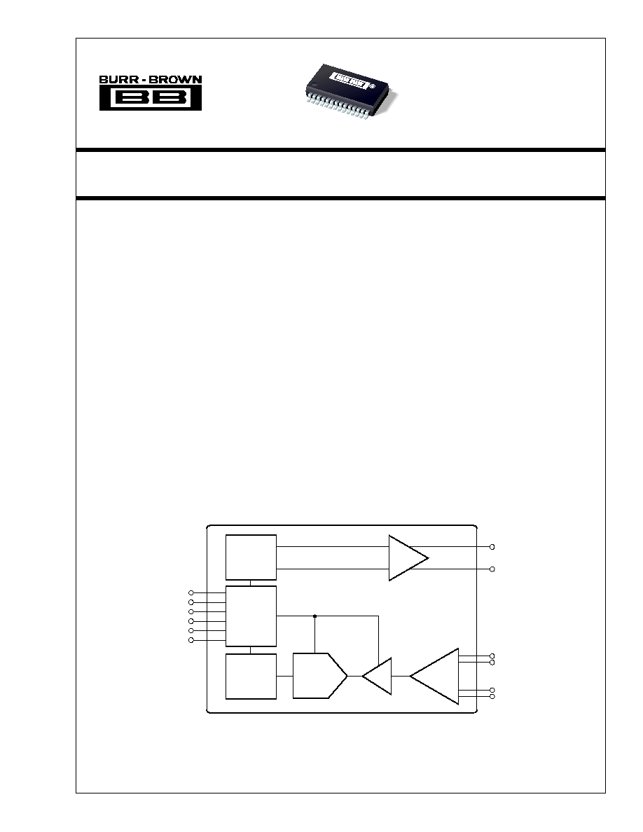
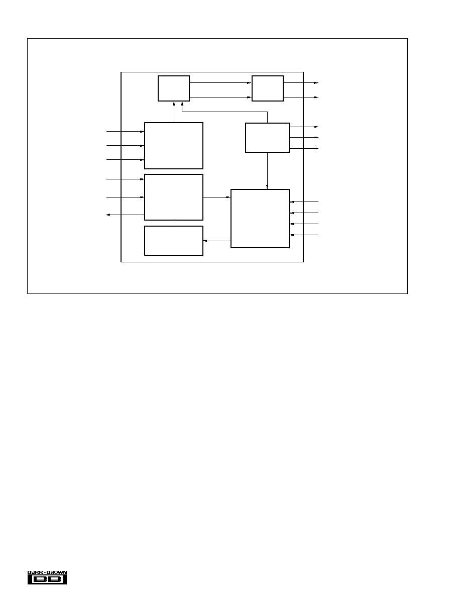
Functionally, this unit consists of a transmit and a
receive section. The transmit section generates analog
signals from 2-bit digital symbol data and filters the
analog signals to create 2B1Q symbols. The on-board
differential line driver provides a 13.5dBm signal to
the telephone line. The receive section filters and
digitizes the symbol data received on the telephone
line. The AFE1224 operates on a single 5V supply.
The digital circuitry in the unit can be connected to a
supply from 3.3V to 5V. The chip uses only 355mW
for full-speed operation. It is housed in a 28-lead
SSOP package.
Modulator
Pulse Former
PGA
Difference
Amplifier
Patents Pending
AFE1224
Line Driver
txLINE
txLINE
rxHYB
rxHYB
rxLINE
rxLINE
tx and rx
Control
Registers
tx and rx
Interface
Lines
Decimation
Filter
AFE1224

2
Æ
AFE1224
SPECIFICATIONS
All specifications at 25
∞
C, AV
DD
= +5V, DV
DD
= +3.3V, f
TX
= 1168kHz (E1 rate) and normal power mode, unless otherwise noted.
The information provided herein is believed to be reliable; however, BURR-BROWN assumes no responsibility for inaccuracies or omissions. BURR-BROWN
assumes no responsibility for the use of this information, and all use of such information shall be entirely at the user's own risk. Prices and specifications are subject
to change without notice. No patent rights or licenses to any of the circuits described herein are implied or granted to any third party. BURR-BROWN does not
authorize or warrant any BURR-BROWN product for use in life support devices and/or systems.
AFE1224E
PARAMETER
COMMENTS
MIN
TYP
MAX
UNITS
RECEIVE CHANNEL
Number of Inputs
Differential
2
Input Voltage Range
Balanced Differential
(1)
±
3.0
V
Common-Mode Voltage
AV
DD
/2
V
Input Impedance, All Inputs
78kbps
32
k
1168kbps
21
k
2320kbps
10
k
Input Capacitance
10
pF
Input Gain Matching
Line Input vs Hybrid Input
±
2
%
Resolution
14
Bits
Programmable Gain
0dB, 3dB, 6dB, 9dB and 12dB
0
+12
dB
Settling Time for Gain Change
6
Symbol Periods
Gain + Offset Error
Tested at Each Gain Range
5
%FSR
(2)
Output Data Coding
Binary Two's Complement
Data Rate
Normal Power
64
2320
kbps
Medium Power
64
1168
kbps
Low Power
64
320
kbps
Output Word Rate
Normal Power
(3)
32
1168
kHz
TRANSMIT CHANNEL
Transmit Clock Rate, f
TX
Symbol Rate, Normal Power
196
1168
kHz
Symbol Rate, Medium Power
96
584
kHz
Symbol Rate, Low Power
80
160
kHz
Transmit ≠3dB Point
2320kbps
485
kHz
1168kbps
292
kHz
784kbps
196
kHz
Transmit Power
(5)
13
13.5
14
dBm
Pulse Output
See Typical Performance Curves
Common-Mode Voltage (V
CM
)
AV
DD
/2
V
Output Resistance
DC to 1MHz
1
TRANSCEIVER PERFORMANCE
Uncancelled Echo
(5)
rxGAIN = 0dB, Loopback Enabled
≠71
≠68.5
dB
rxGAIN = 0dB, Loopback Disabled
≠71
≠68.5
dB
rxGAIN = 3dB, Loopback Disabled
≠74
≠71
dB
rxGAIN = 6dB, Loopback Disabled
≠76
≠73.5
dB
rxGAIN = 9dB, Loopback Disabled
≠78
≠75.5
dB
rxGAIN = 12dB, Loopback Disabled
≠80
≠77.5
dB
DIGITAL INTERFACE
Logic Levels
V
IH
|I
IH
| < 10
µ
A
DV
DD
≠1
DV
DD
+0.3
V
V
IL
|I
IL
| < 10
µ
A
≠0.3
+0.8
V
V
OH
I
OH
= ≠20
µ
A
DV
DD
≠0.5
V
V
OL
I
OL
= 20
µ
A
+0.4
V
t
rx1
Interface
3
4.6
ns
POWER
Analog Power Supply Voltage
Specification
5
V
Operating Range
4.75
5.25
V
Digital Power Supply Voltage
Specification
3.3
V
Operating Range
3.15
5.25
V
Power Dissipation
(4, 5)
Normal Power
385
mW
Medium Power
300
mW
Low Power
240
mW
Power Dissipation
(4, 5)
Normal Power, DV
DD
= 5V
415
mW
Power Supply Rejection Ratio
55
dB
TEMPERATURE RANGE
Operating
(6)
≠40
+85
∞
C
NOTES: (1) With a balanced differential signal, the positive input is 180
∞
out-of-phase with the negative input, therefore the actual voltage swing about the common-
mode voltage on each pin is
±
1.5V to achieve a total input range of
±
3.0V or 6Vp-p. (2) FSR is Full-Scale Range. (3) The output data is available at twice the symbol
rate with interpolated values. (4) With a pseudo-random equiprobable sequence of HDSL pulses; 13.5dBm applied to the transformer (16.5dBm output from txLINE+
and txLINE≠). (5) See the Discussion of Specifications section of this data sheet for more information. (6) Functionality only guaranteed over temperature range.
3
Æ
AFE1224
PIN CONFIGURATION
Analog Inputs: Current ..............................................
±
100mA, Momentary
±
10mA, Continuous
Voltage .................................. AGND ≠0.3V to AV
DD
+0.3V
Analog Outputs Short Circuit to Ground (+25
∞
C) ..................... Continuous
AV
DD
to AGND ......................................................................... ≠0.3V to 6V
DV
DD
to DGND ......................................................................... ≠0.3V to 6V
Digital Input Voltage to DGND .................................. ≠0.3V to DV
DD
+0.3V
Digital Output Voltage to DGND ............................... ≠0.3V to DV
DD
+0.3V
AGND, DGND, Differential Voltage .................................................... 0.3V
Junction Temperature (T
J
) ............................................................. +150
∞
C
Storage Temperature Range .......................................... ≠40
∞
C to +125
∞
C
Lead Temperature (soldering, 3s) .................................................. +260
∞
C
Power Dissipation .......................................................................... 700mW
ABSOLUTE MAXIMUM RATINGS
ELECTROSTATIC
DISCHARGE SENSITIVITY
This integrated circuit can be damaged by ESD. Burr-Brown
recommends that all integrated circuits be handled with
appropriate precautions. Failure to observe proper handling
and installation procedures can cause damage.
ESD damage can range from subtle performance degradation
to complete device failure. Precision integrated circuits may
be more susceptible to damage because very small parametric
changes could cause the device not to meet its published
specifications.
PACKAGE
SPECIFIED
DRAWING
TEMPERATURE
PACKAGE
ORDERING
TRANSPORT
PRODUCT
PACKAGE
NUMBER
(1)
RANGE
MARKING
NUMBER
(2)
MEDIA
AFE1224E
SSOP-28
324
≠40
∞
C to +85
∞
C
AFE1224E
AFE1224E
Rails
"
"
"
"
"
AFE1224E/1K
Tape and Reel
NOTES: (1) For detailed drawing and dimension table, please see end of data sheet, or Appendix C of Burr-Brown IC Data Book. (2) Models with a slash (/ ) are
available only in Tape and Reel in the quantities indicated (e.g., /1K indicates 1000 devices per reel). Ordering 1000 pieces of "AFE1224E/1K" will get a single 1000-
piece Tape and Reel. For detailed Tape and Reel mechanical information, refer to Appendix B of Burr-Brown IC Data Book.
PACKAGE/ORDERING INFORMATION
Top View
SSOP-28
PIN #
TYPE
NAME
DESCRIPTION
1
--
NC
No Connection
2
--
NC
No Connection
3
Power
DV
DD
Digital Supply (+3.3 to +5V)
4
Ground
DGND
Digital Ground
5
Input
txbaudCLK
Transmit Baud Clock
6
Input
tx48xCLK
Transmit Clock at 48x Baud Clock
7
Input
Data In
Input Data Word
8
Input
rxbaudCLK
Receive Baud Clock
9
Input
rx48xCLK
Receive Clock at 48x Baud Clock
10
Output
Data Out
Output Data Word
11
Power
DV
DD
Digital Supply (+3.3V to +5V)
12
Ground
DGND
Digital Ground
13
Power
AV
DD
Analog Supply (+5V)
14
Input
rxHYB≠
Negative Input from Hybrid Network
15
Input
rxHYB+
Positive Input from Hybrid Network
16
Input
rxLINE≠
Negative Line Input
17
Input
rxLINE+
Positive Line Input
18
Ground
AGND
Analog Ground
19
Output
vrREF+
Positive Reference Output
20
Output
V
CM
Common-Mode Voltage (buffered)
21
Output
vrREF≠
Negative Reference Output
22
Power
AV
DD
Analog Supply (+5V)
23
Ground
AGND
Analog Ground
24
Output
txLINE≠
Negative Line Output
25
Power
AV
DD
Output Buffer Supply (+5V)
26
Output
txLINE+
Positive Line Output
27
Ground
AGND
Output Buffer Ground
28
--
NC
No Connection
PIN DESCRIPTIONS
NC
NC
DV
DD
DGND
txbaudCLK
tx48xCLK
Data In
rxbaudCLK
rx48xCLK
Data Out
DV
DD
DGND
AV
DD
rxHYB≠
NC
AGND
txLINE+
AV
DD
txLINE≠
AGND
AV
DD
vrREF≠
V
CM
vrREF+
AGND
rxLINE+
rxLINE≠
rxHYB+
1
2
3
4
5
6
7
8
9
10
11
12
13
14
28
27
26
25
24
23
22
21
20
19
18
17
16
15
AFE1224
4
Æ
AFE1224
BLOCK DIAGRAM
Pulse
Former
Filter
txbaudCLK
tx48xCLK
Data In
rxbaudCLK
rx48xCLK
Data Out
Output
Buffer
Voltage
Reference
Modulator
Transmit
Control
Receive
Control
Decimation
Filter
txLINE≠
txLINE+
REF+
V
CM
REF≠
rxLINE+
rxLINE≠
rxHYB+
rxHYB≠
5
Æ
AFE1224
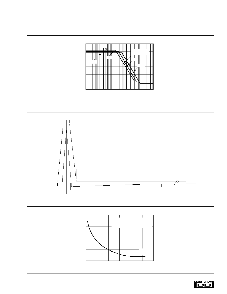
TYPICAL PERFORMANCE CURVES
At Output of HDSL Pulse Transformer
The curves shown below are measured at the line output of the HDSL transformer. Typical at 25
∞
C, AV
DD
+ = +5V, DV
DD
+ = +3.3V, and f
TX
= 1168kHz, unless otherwise specified.
CURVE 1. Upper Bound of Power Spectral Density Measured at Output of HDSL Transformer.
CURVE 3. Input Impedance of rxLINE and rxHYB.
CURVE 2. Transmitted Pulse Template Measured at HDSL Transformer Output.
0.4T 0.4T
≠0.6T
≠1.2T
14T
50T
0.5T
1.25T
1k
≠20
≠40
≠60
≠80
≠100
≠120
≠140
10k
100k
100M
AVERAGE POWER SPECTRAL DENSITY LIMIT
Power Spectral Density (dBm/Hz)
Frequency (Hz)
1M
10M
T1
E1-SP
≠80dB/decade
E1
E1-SP
E1
T1
200
100
75
50
25
0
600
1000
INPUT IMPEDANCE vs BIT RATE
Input Impedance (k
)
Bit Rate (kbps)
1400
1800
2600
2200
E1
T1
Two Pair T1 = 784kbps, 32k
Two Pair E1 = 1168kbps, 21k
Single Pair E1 = 2320kbps, 10k
E1,
Single Pair