Äîêóìåíòàöèÿ è îïèñàíèÿ www.docs.chipfind.ru
SBOS277E - JUNE 2004 - REVISED DECEMBER 2004
18 V SUPPLY MULTI CHANNEL GAMMA CORRECTION BUFFER
BUF05704, BUF06704
BUF07704, BUF11704
FEATURES
D
Wide Supply Range: 4.5 V to 18 V
D
Gamma Correction Channels: 10, 6, and 4
D
Integrated V
COM
Buffer
D
Excellent Output Current Drive:
- Gamma Channels:
> 30 mA at 0.5 V Swing to Rails
(1)
- V
COM
:
> 100 mA typ at 2 V Swing to Rails
(1)
D
Large Capacitive Load Drive Capability
D
Rail-to-Rail Output
D
PowerPAD
Package
D
Low-Power/Channel: < 500
µ
A
D
High ESD Rating: 8 kV HBM, 2 kV CDM,
300 V MM
D
Specified for -25
°
C to +85
°
C
(1) See Typical Characteristic curves for details.
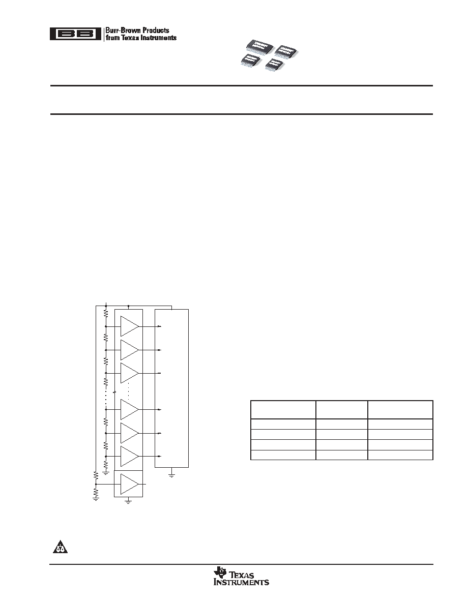
BUFx x704
V
DD
V
COM
So urce Driver
Gamma 1
Gamma 2
Gamma 3
Gamma (n
-
2)
Gamma (n
-
1)
Gamma (n )
DESCRIPTION
The BUFxx704 are a series of multi-channel buffers
targeted towards gamma correction in high-resolution
LCD panels. They are pin-compatible with the existing
BUFxx702 and BUFxx703 family and operate at higher
supply voltages up to 18 V (19 V absolute max). The
higher supply voltage enables faster response times
and brighter images in large-screen LCD panels. This
is especially important in LCD TV applications.
The number of gamma correction channels required
depends on a variety of factors and differs greatly from
design to design. Therefore, 10, 6, and 4 channel
options are offered. For additional space and cost
savings, a V
COM
channel with > 100mA drive capability
is integrated into the BUF11704, BUF07704, and
BUF05704.
The BUF11704, BUF07704, BUF06704, and
BUF05704 are available in the TSSOP-28, TSSOP-20,
TSSOP-16, and TSSOP-14 PowerPAD packages for
dramatically increased power dissipation capability.
This way, a large number of channels can be handled
safely in one package.
A flow-through pin out has been adopted to allow simple
PCB routing and maintain the cost-effectiveness of this
solution. All inputs and outputs of the BUFxx704
incorporate internal ESD protection circuits that prevent
functional failures at voltages up to 8 kV (HBM), 2 kV
(CDM), and 300 V (MM).
MODEL
GAMMA
CHANNELS
VCOM CHANNELS
BUF11704
10
1
BUF07704
6
1
BUF06704
6
0
BUF05704
4
1
www.ti.com
Copyright
2004, Texas Instruments Incorporated
Please be aware that an important notice concerning availability, standard warranty, and use in critical applications of Texas Instruments
semiconductor products and disclaimers thereto appears at the end of this data sheet.
PRODUCTION DATA information is current as of publication date. Products
conform to specifications per the terms of Texas Instruments standard warranty.
Production processing does not necessarily include testing of all parameters.
PowerPAD is a trademark of Texas Instruments Incorporated. All other trademarks are the property of their respective owners.
BUF05704, BUF06704
BUF07704, BUF11704
SBOS277E - JUNE 2004 - REVISED DECEMBER 2004
www.ti.com
2
ABSOLUTE MAXIMUM RATINGS
over operating free-air temperature range unless otherwise noted(1)
PARAMETERS
BUFxx704
UNIT
Supply Voltage, VDD(2)
19
V
Input Voltage Range, VI
±
VDD
Continuous Total Power Dissipation
See Dissipation Rating Table
Operating Free-Air Temperature Range, TA
-25 to 85
°
C
Maximum Junction Temperature, TJ
125
°
C
Storage Temperature Range, TSTG
-65 to 150
°
C
Lead Temperature 1.6mm (1/16 inch) from Case for 10s
260
°
C
ESD Rating:
Human Body Model (HBM)
8
kV
Charged-Device Model (CDM)
2
kV
Machine Model (MM)
300
V
(1) Stresses beyond those listed under absolute maximum ratings may cause permanent damage to the device. These are stress ratings only, and
functional operation of the device at these or any other conditions beyond those indicated under recommended operating conditions is not
implied. Exposure to absolute-maximum-rated conditions for extended periods may affect device reliability.
(2) All voltage values are with respect to GND.
ORDERING INFORMATION
(1)
PRODUCT
PACKAGE-LEAD
PACKAGE MARKING
BUF05704
TSSOP-14
BUF05704
BUF05704
TSSOP-14
BUF05704
BUF06704
TSSOP-16
BUF06704
BUF06704
TSSOP-16
BUF06704
BUF07704
TSSOP-20
BUF07704
BUF07704
TSSOP-20
BUF07704
BUF11704
TSSOP-28
BUF11704
BUF11704
TSSOP-28
BUF11704
(1) For the most current package and ordering information, see the Package Option Addendum located at the end of this data sheet.
DISSIPATION RATING TABLE
PACKAGE TYPE
PACKAGE
DESIGNATOR
JC
(1)
(
°
C/W)
q
JA
(1)
(
°
C/W)
TA
25
°
C
POWER RATING
TSSOP-28
PWP (28)
0.72
27.9
3.58 W
TSSOP-20
PWP (20)
1.40
32.63
3.06 W
TSSOP-16
PWP (16)
2.07
36.51
2.74
TSSOP-14
PWP (14)
2.07
37.47
2.67
(1) PowerPAD attached to PCB, 0 lfm airflow, and 76mm x 76mm copper area.
RECOMMENDED OPERATING CONDITIONS
MIN
NOM
MAX
UNIT
Supply Voltage, VDD
7
18
V
Operating Free-Air Temperature, TA
-25
+85
°
C
BUF05704, BUF06704
BUF07704, BUF11704
SBOS277E - JUNE 2004 - REVISED DECEMBER 2004
www.ti.com
3
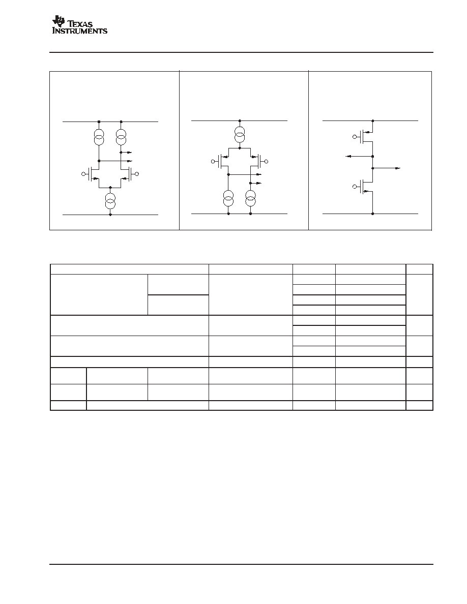
EQUIVALENT SCHEMATICS OF INPUTS AND OUTPUTS
Buffer
Input
Buffer
Output
Next Stage
Next Stage
V
S
GND
Internal to BUF11704
INPUT STAGE OF BUFFERS
BUF11704: 1 to 5 and V
COM
BUF07704: 1 to 3 and V
COM
BUF06704: 1 to 3
BUF05704: 1 to 2 and V
COM
Buffer
Input
Buffer
Output
Next Stage
Next Stage
V
S
GND
Internal to BUF11704
INPUT STAGE OF BUFFERS
BUF11704: 6 to 10
BUF07704: 4 to 6
BUF06704: 4 to 6
BUF05704: 3 to 4
Previous
Stage
Previous
Stage
Inverting
Input
Buffer
Output
V
S
GND
OUTPUT STAGE OF ALL BUFFERS
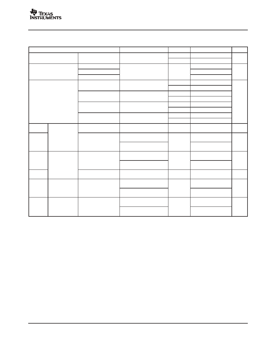
ELECTRICAL CHARACTERISTICS: BUFxx704
Over operating free-air temperature range, VDD = 18 V, TA = 25
°
C, unless otherwise noted.
PARAMETER
TEST CONDITIONS
TA
MIN
TYP
MAX
UNIT
Gamma buffers
25
°
C
-1
20
VIO
Input offset voltage
Gamma buffers
VI = 9V
Full range(1)
20
mV
VIO
Input offset voltage
VCOM
VI = 9V
25
°
C
-1
30
mV
VCOM
Full range(1)
30
IIB
Input bias current
VI = VDD/2
25
°
C
1
pA
IIB
Input bias current
VI = VDD/2
Full range(1)
200
pA
PSRR
Power-Supply Rejection Ratio
VDD = 4.5 V to 19 V
25
°
C
62
80
dB
PSRR
Power-Supply Rejection Ratio
VDD = 4.5 V to 19 V
Full range(1)
60
dB
Buffer gain
VI = 5 V
25
°
C
0.9995
V/V
BW_3dB
3dB bandwidth
Gamma buffers
VCOM buffer
CL = 100 pF, RL = 2 k
25
°
C
1
0.6
MHz
SR
Slew rate
Gamma buffers
VCOM buffer
CL = 100 pF, RL = 2 k
VIN = 2 V to 16 V
25
°
C
1.6
4.6
V/
µ
s
Crosstalk
VIP-P = 6 V, f = 1 kHz
25
°
C
85
dB
(1) Full range is -25
°
C to 85
°
C.
BUF05704, BUF06704
BUF07704, BUF11704
SBOS277E - JUNE 2004 - REVISED DECEMBER 2004
www.ti.com
4
ELECTRICAL CHARACTERISTICS: BUF11704
Over operating free-air temperature range, VDD = 18 V, TA = 25
°
C, unless otherwise noted.
PARAMETER
TEST CONDITIONS
TA(1)
MIN
TYP
MAX
UNIT
IDD
Supply current
ALL
VO = VDD/2
25
°
C
5
9.0
mA
IDD
Supply current
ALL
VO = VDD/2
No Load
Full range
9.0
mA
Buffers 1-5
1
VDD
Common-mode input range
Buffers 6-10
25
°
C
GND
VDD - 1
V
Common-mode input range
VCOM buffer
25 C
1
VDD
V
VCOM buffer sinking
IO = 1 mA to 100 mA,
25
°
C
1
5
VCOM buffer sinking
IO = 1 mA to 100 mA,
VIN = 2 V
Full range
5
VCOM buffer sourcing
IO = -1 mA to -100 mA
25
°
C
1
5
Load regulation
VCOM buffer sourcing
IO = -1 mA to -100 mA
VIN = 16 V
Full range
5
mV/mA
Load regulation
Buffers 1-10 sinking
IO = 1 mA to 10 mA
25
°
C
1
5
mV/mA
Buffers 1-10 sinking
IO = 1 mA to 10 mA
VIN = 1 V
Full range
5
Buffers 1-10 sourcing
IO = -1 mA to -10 mA
25
°
C
1
5
Buffers 1-10 sourcing
IO = -1 mA to -10 mA
VIN = 17 V
Full range
5
VOH1-5
Buffers 1-5
VIN = 18 V
ISOURCE = 10 mA
25
°
C
17.85
17.9
V
VOH6-10
High-level output
voltage
Buffers 6-10
VIN = 17 V
ISINK = 10 mA
25
°
C
17
17.15
V
VOH6-10
voltage
Buffers 6-10
VIN = 17 V
ISOURCE = 10 mA
25
°
C
16.85
17
V
VOL1-5
Buffers 1-5
VIN = 1 V
ISINK = 10 mA
25
°
C
1.0
1.15
V
VOL1-5
Low-level output
voltage
Buffers 1-5
VIN = 1 V
ISOURCE = 10 mA
25
°
C
0.85
1.0
V
VOL6-10
voltage
Buffers 6-10
VIN = 0 V
ISINK = 10 mA
25
°
C
0
0.15
V
VOHCOM
High-level output
voltage
VCOM buffer
VIN = 16 V
ISINK = 100 mA
25
°
C
16
16.15
V
VOHCOM
High-level output
voltage
VCOM buffer
VIN = 16 V
ISOURCE = 100 mA
25
°
C
15.85
16
V
VOLCOM
Low-level output
voltage
VCOM buffer
VIN = 2 V
ISINK = 100 mA
25
°
C
2
2.15
V
VOLCOM
Low-level output
voltage
VCOM buffer
VIN = 2 V
ISOURCE = 100 mA
25
°
C
1.85
2
V
(1) Full range is -25
°
C to 85
°
C.
BUF05704, BUF06704
BUF07704, BUF11704
SBOS277E - JUNE 2004 - REVISED DECEMBER 2004
www.ti.com
5
ELECTRICAL CHARACTERISTICS: BUF07704
Over operating free-air temperature range, VDD = 18 V, TA = 25
°
C, unless otherwise noted.
PARAMETER
TEST CONDITIONS
TA(1)
MIN
TYP
MAX
UNIT
IDD
Supply current
ALL
VO = VDD/2
25
°
C
5
7.5
mA
IDD
Supply current
ALL
VO = VDD/2
No Load
Full range
7.5
mA
Buffers 1-3
1
VDD
Common-mode input range
Buffers 4-6
25
°
C
GND
VDD - 1
V
Common-mode input range
VCOM buffer
25 C
1
VDD
V
VCOM buffer sinking
IO = 1 mA to 100 mA
25
°
C
1
5
VCOM buffer sinking
IO = 1 mA to 100 mA
VIN = 2 V
Full range
5
VCOM buffer sourcing
IO = -1 mA to -100 mA
25
°
C
1
5
Load regulation
VCOM buffer sourcing
IO = -1 mA to -100 mA
VIN = 16 V
Full range
5
mV/mA
Load regulation
Buffers 1-6 sinking
IO = 1 mA to 10 mA
25
°
C
1
5
mV/mA
Buffers 1-6 sinking
IO = 1 mA to 10 mA
VIN = 1 V
Full range
5
Buffers 1-6 sourcing
IO = -1 mA to -10 mA
25
°
C
1
5
Buffers 1-6 sourcing
IO = -1 mA to -10 mA
VIN = 17 V
Full range
5
VOH1-3
Buffers 1-3
VIN = 18 V
ISOURCE = 10 mA
25
°
C
17.85
17.9
V
VOH4-6
High-level output
voltage
Buffers 4-6
VIN = 17 V
ISINK = 10 mA
25
°
C
17
17.15
V
VOH4-6
voltage
Buffers 4-6
VIN = 17 V
ISOURCE = 10 mA
25
°
C
16.85
17
V
VOL1-3
Buffers 1-3
VIN = 1 V
ISINK = 10 mA
25
°
C
1.0
1.15
V
VOL1-3
Low-level output
voltage
Buffers 1-3
VIN = 1 V
ISOURCE = 10 mA
25
°
C
0.85
1.0
V
VOL4-6
voltage
Buffers 4-6
VIN = 0 V
ISINK = 10 mA
25
°
C
0
0.15
V
VOHCOM
High-level output
voltage
VCOM buffer
VIN = 16 V
ISINK = 100 mA
25
°
C
16
16.15
V
VOHCOM
High-level output
voltage
VCOM buffer
VIN = 16 V
ISOURCE = 100 mA
25
°
C
15.85
16
V
VOLCOM
Low-level output
voltage
VCOM buffer
VIN = 2 V
ISINK = 100 mA
25
°
C
2
2.15
V
VOLCOM
Low-level output
voltage
VCOM buffer
VIN = 2 V
ISOURCE = 100 mA
25
°
C
1.85
2
V
(1) Full range is -25
°
C to 85
°
C.