 | –≠–ª–µ–∫—Ç—Ä–æ–Ω–Ω—ã–π –∫–æ–º–ø–æ–Ω–µ–Ω—Ç: DAC4813 | –°–∫–∞—á–∞—Ç—å:  PDF PDF  ZIP ZIP |

Æ
DAC4813
1
DAC4813
DAC4813
QUAD 12-BIT DIGITAL-TO-ANALOG
CONVERTER (12-bit port interface)
Æ
© 1992 Burr-Brown Corporation
PDS-1148C
Printed in U.S.A. May, 1997
FEATURES
q
COMPLETE WITH REFERENCE AND
OUTPUT AMPLIFIERS
q
12-BIT PORT INTERFACE
q
ANALOG OUTPUT RANGE:
±
10V
q
MONOTONICITY GUARANTEED OVER
TEMPERATURE
q
INTEGRAL LINEARITY
ERROR:
±
1/2LSB max
q
±
12V to
±
15V SUPPLIES
q
28-PIN PLASTIC DIP PACKAGE
DESCRIPTION
DAC4813 is a complete quad 12-bit digital-to-analog
converter with bus interface logic. Each package in-
cludes a precision +10V voltage reference, double-
buffered bus interface including a RESET function
and 12-bit D/A converters with voltage-output opera-
tional amplifiers.
The double-buffered interface consists of a 12-bit
input latch and a D/A latch for each D/A converter. A
RESET control allows the D/A outputs to be asyn-
chronously reset to bipolar zero, a feature useful for
power-up reset, system initialization and recalibration.
DAC4813 D/A converters are committed to the
±
10V
output range only. Gain and offset are not externally
adjustable.
DAC4813 is available with a integral linearity error of
1/2LSB and 12-bit monotonicity guaranteed over tem-
perature. It is packaged in a 28-pin 0.6in. wide plastic
DIP package and specified over ≠40
o
C to +85
o
C and
0
∞
C to +70
∞
C.
V
REF OUT
V
OUT 1
D/A 1
DB0
DB11
LSB
MSB
12
V
OUT 2
D/A 2
V
OUT 3
D/A 3
V
OUT 4
D/A 4
DAC4813
10V
Reference
12-bit
Latches
International Airport Industrial Park ∑ Mailing Address: PO Box 11400, Tucson, AZ 85734 ∑ Street Address: 6730 S. Tucson Blvd., Tucson, AZ 85706 ∑ Tel: (520) 746-1111 ∑ Twx: 910-952-1111
Internet: http://www.burr-brown.com/ ∑ FAXLine: (800) 548-6133 (US/Canada Only) ∑ Cable: BBRCORP ∑ Telex: 066-6491 ∑ FAX: (520) 889-1510 ∑ Immediate Product Info: (800) 548-6132
Æ
DAC4813
2
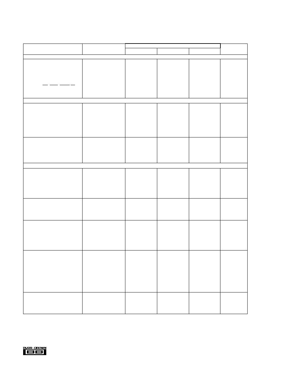
SPECIFICATIONS
ELECTRICAL
T
A
= +25
o
C, +V
CC
= +12V or +15V, ≠V
CC
= ≠12V or ≠15V, unless otherwise noted.
DAC4813AP, JP
PARAMETER
CONDITIONS
MIN
TYP
MAX
UNITS
INPUTS
DIGITAL INPUTS
Over Temperature
Input Code
(1)
Range
Bipolar Offset Binary
Logic Levels
(2)
V
IH
(3)
+2
+5.5
V
V
IL
0
+0.8
V
Logic Input Currents
DB0-DB11, WR, LDAC, RESET,EN
X
I
IH
V
I
= +2.7V
±
40
µ
A
I
IL
V
I
= +0.4V
±
40
µ
A
TRANSFER CHARACTERISTICS
ACCURACY
Linearity Error
±
1/4
±
1/2
LSB
Differential Linearity Error
±
1/2
±
1
LSB
Gain Error
±
0.05
±
0.2
%
Bipolar Zero Error
(5)
±
0.05
±
0.2
%FSR
(4)
Power Supply Sensitivity
Of Full Scale +V
CC
±
5
±
20
ppmFSR/%+V
CC
≠V
CC
±
1
±
10
ppmFSR/%≠V
CC
DRIFT
Over Specification
Temperature Range
Gain
±
5
±
30
ppm/
∞
C
Bipolar Zero Drift
±
5
±
15
ppmFSR/
∞
C
Linearity Error over Temperature
±
1/2
±
3/4
LSB
Monotonicity
Guaranteed
DYNAMIC CHARACTERISTICS
SETTLING TIME
(6)
To within
±
0.012%FSR
of Final Value
5k
|| 500pF Load
Full Scale Range Change
20V Range
4.5
6
µ
s
1LSB Output Step
(7)
At Major Carry
2
µ
s
Slew Rate
10
V/
µ
s
Crosstalk
(8)
5k
Loads
0.2
LSB
OUTPUT
Output Voltage Range
±
V
CC
±
11.4V
±
10
V
Output Current
±
5
mA
Output Impedance
0.2
Short Circuit to ACOM Duration
at DC
Indefinite
REFERENCE VOLTAGE
Voltage
+9.95
+10.00
+10.05
V
Source Current Available
for External Loads
2
mA
Impedance
0.2
Temperature Coefficient
±
5
±
25
ppm/
∞
C
Short Circuit to Common Duration
at DC
Indefinite
POWER SUPPLY REQUIREMENTS
Voltage: +V
CC
+11.4
+15
+16.5
V
≠V
CC
≠11.4
≠15
≠16.5
V
Current:
No Load
±
V
CC
=
±
15V
+V
CC
48
60
mA
≠V
CC
24
28
mA
Power Dissipation
1080
1320
mW
Potential at DCOM with
Respect to ACOM
(9)
≠3
+3
V
TEMPERATURE RANGES
Specification: AP
≠40
+85
∞
C
JP
0
+70
∞
C
Storage
≠60
+100
∞
C
Thermal Resistance,
JA
,Plastic DIP
30
∞
C/W
NOTES: (1) For Two's Complement Input Coding invert the MSB with an external logic inverter. (2) Digital inputs are TTL and +5V CMOS compatible over the specification
temperature range. (3) Open DATA input lines will be pulled above +5.5V. See discussion under LOGIC INPUT COMPATIBILITY in the OPERATION section. (4) FSR
means Full Scale Range. For example, for
±
10V output, FSR = 20V. (5) Error at input code 800
HEX
. (6) Maximum represents the 3
limit. Not 100% tested for this
parameter. (7) For the worst-case code change: 7FF
HEX
to 800
HEX
and 800
HEX
to 7FF
HEX
. (8) Crosstalk is defined as the change in any output as a result of any other
output being driven from ≠10V to +10V at rated output current. (9) The maximum voltage at which ACOM and DCOM may be separated without affecting accuracy
specifications.

Æ
DAC4813
3
ABSOLUTE MAXIMUM RATINGS
+V
CC
to ACOM ............................................................................ 0 to +18V
≠V
CC
to ACOM ............................................................................ 0 to ≠18V
+V
CC
to ≠V
CC
............................................................................... 0 to +36V
ACOM to DCOM ..................................................................................
±
4V
Digital Inputs to DCOM ........................................................... ≠1V to +V
CC
External Voltage applied to BPO Resistor .........................................
±
18V
V
REF OUT
.............................................................. Indefinite short to ACOM
V
OUT
............................................................................ Momentary to
±
18V
Lead Temperature, soldering 10s .................................................. +300
o
C
Max Junction Temperature .............................................................. 165
o
C
NOTE: Stresses above those listed under "Absolute Maximum Ratings" may
cause permanent damage to the device. Exposure to absolute maximum
conditions for extended periods may affect device reliability.
PACKAGE
DRAWING
TEMPERATURE
PRODUCT
PACKAGE
NUMBER
(1)
RANGE
DAC4813AP
28-Pin Plastic DBL Wide DIP
215
≠40
∞
C to +85
∞
C
DAC4813JP
28-Pin Plastic DBL Wide DIP
215
0
∞
C to +70
∞
C
NOTE: (1) For detailed drawing and dimension table, please see end of data
sheet, or Appendix C of Burr-Brown IC Data Book.
PACKAGE/ORDERING INFORMATION
ELECTROSTATIC
DISCHARGE SENSITIVITY
Electrostatic discharge can cause damage ranging from per-
formance degradation to complete device failure. Burr-Brown
Corporation recommends that all integrated circuits be handled
and stored using appropriate ESD protection methods.
TIMING DIAGRAMS
> 5ns
> 50ns
> 50ns
(Load first rank from Data Bus: LDAC = 1)
DB11≠DB0
WR
> 50ns
WRITE CYCLE #1
EN
X
t
SETTLING
±1/2LSB
LDAC
WR
> 50ns
> 50ns
V
OUT
WRITE CYCLE #2
(Load second rank from first rank: EN
X
= 1)
±1/2LSB
Reset
> 50ns
+10V
≠10V
0V
t
SETTLING
V
OUT
RESET COMMAND (Bipolar Mode)
EN
X
, LDAC, WR = Don't Care
TRUTH TABLE
WR
EN1
EN2
EN3
EN4
LDAC
RESET
OPERATION
X
X
X
X
X
X
0
Reset all D/A Latches
1
X
X
X
X
X
1
No Operation
X
1
1
1
1
1
1
No Operation
0
1
1
1
0
1
1
Load Data into First Rank for D/A 4
0
1
1
0
1
1
1
Load Data into First Rank for D/A 3
0
1
0
1
1
1
1
Load Data into First Rank for D/A 2
0
0
1
1
1
1
1
Load Data into First Rank for D/A 1
0
1
1
1
1
0
1
Load Second Rank from First Rank, All D/As
0
0
0
0
0
0
1
All Latches Transparent
"X" = Don't Care

Æ
DAC4813
4
PIN DESCRIPTIONS
PIN
NAME
FUNCTION
1
DB11
DATA, MSB, positive true.
2
DB10
DATA
3
DB9
DATA
4
DB8
DATA
5
DB7
DATA
6
DB6
DATA
7
DB5
DATA
8
DB4
DATA
9
DB3
DATA
10
DB2
DATA
11
DB1
DATA
12
DB0
DATA, LSB.
13
RESET
Resets output of all D/As to bipolar-zero. The D/A remains in this state until overwritten by a LDAC-WR command. RESET
does not reset the input latch. After power≠up and reset, input latches will be in an indeterminant state.
14
WR
Write strobe. Must be low for data transfer to any latch (except RESET).
15
EN1
Enable for 12-bit input data latch of D/A1. NOTE: This logic path is slower than the WR/ path.
16
EN2
Enable for 12-bit input data latch of D/A2. NOTE: This logic path is slower than the WR/ path.
17
EN3
Enable for 12-bit input data latch of D/A3. NOTE: This logic path is slower than the WR /path.
18
EN4
Enable for 12-bit input data latch of D/A4. NOTE: This logic path is slower than the WR/ path.
19
LDAC
Load DAC enable. Must be low with WR for data transfer to the D/A latch and simultaneous update of all D/A converters.
20
DCOM
Digital common, logic currents return.
21
≠V
CC
Analog supply input, nominally ≠12V or ≠15V referred to ACOM.
22
ACOM
Analog common, +V
CC
, ≠V
CC
supply return.
23
+V
CC
Analog supply input, nominally +12V or +15V referred to ACOM.
24
V
OUT
4
D/A 4 analog output.
25
V
OUT
3
D/A 3 analog output.
26
V
OUT
2
D/A 2 analog output.
27
V
OUT
1
D/A 1 analog output.
28
V
REF OUT
+10V reference output.
The information provided herein is believed to be reliable; however, BURR-BROWN assumes no responsibility for inaccuracies or omissions. BURR-BROWN assumes
no responsibility for the use of this information, and all use of such information shall be entirely at the user's own risk. Prices and specifications are subject to change
without notice. No patent rights or licenses to any of the circuits described herein are implied or granted to any third party. BURR-BROWN does not authorize or warrant
any BURR-BROWN product for use in life support devices and/or systems.

Æ
DAC4813
5
BLOCK DIAGRAM
LSB
DB0
25k
25k
12-Bit D/A Converter
27
1
2
3
4
5
6
7
8
9
10
11
12
MSB
DB11
50k
28
+10V
Reference
22
23
21
+V
CC
≠V
CC
ACOM
V
REF OUT
WR
14
EN
1
15
12-Bit Input Latch
V
OUT 1
0≠800µA
12
12
20
DCOM
25k
25k
12-Bit D/A Converter
26
50k
EN
2
16
12-Bit Input Latch
V
OUT 2
0≠800µA
12
25k
25k
12-Bit D/A Converter
25
50k
EN
3
17
12-Bit Input Latch
V
OUT 3
0≠800µA
12
25k
25k
12-Bit D/A Converter
24
50k
EN
4
18
12-Bit Input Latch
V
OUT 4
0≠800µA
LDAC
19
RESET
13
12-Bit D/A Latch
12-Bit D/A Latch
12-Bit D/A Latch
12-Bit D/A Latch
NOTE: RESET does not reset input latches.