 | –≠–ª–µ–∫—Ç—Ä–æ–Ω–Ω—ã–π –∫–æ–º–ø–æ–Ω–µ–Ω—Ç: DAC667JP | –°–∫–∞—á–∞—Ç—å:  PDF PDF  ZIP ZIP |

1
Æ
DAC667
DAC667
Æ
Microprocessor-Compatible
12-BIT DIGITAL-TO-ANALOG CONVERTER
DESCRIPTION
The DAC667 is a complete monolithic integrated cir-
cuit microprocessor-compatible 12-bit digital-to-ana-
log converter. It includes a precision voltage reference,
microcomputer interface logic, double-buffered latch,
and a 12-bit D/A converter with a voltage output
amplifier. Fast current switches and a laser-trimmed
thin-film resistor network provide a highly accurate
and fast D/A converter.
A double-buffered latch facilitates microcomputer inter-
facing to 4-, 8-, 12-, or 16-bit data buses. The input
buffer latch holds the 12-bit data until it is transferred
to an internal 12-bit D/A converter latch, giving precise
timing control over an analog output change.
The DAC667 is specified to
±
1/2LSB maximum lin-
earity error at +25
∞
C. The DAC667 is guaranteed
monotonic over the specification temperature range.
The DAC667 is available in 28-pin, 0.6" wide plastic
DIP package.
FEATURES
q
±
3/4LSB MAX NONLINEARITY OVER
TEMPERATURE
q
MONOTONICITY GUARANTEED OVER
TEMPERATURE
q
MICROCOMPUTER INTERFACE:
Double-Buffered Latch
q
VOLTAGE OUTPUT:
±
10V,
±
5V, +10V
With
±
12V to
±
15V Supplies
q
LOW POWER DISSIPATION: 345mW typ
q
PIN COMPATIBLE WITH AD667
AGND
Ref Out
Ref In
A3
A0
A1
A2
CS
DB11
MSB
DB0
LSB
20V Span
9.95k
5k
5k
10V Span
Reference
OUT
V
19.95k
28
27
26
25
24
23
22
21
20
19
18
17
Power Gnd
+V
CC
≠V
EE
12-Bit D/A Converter
12-Bit Parallel Latch
4 Bits
4 Bits
4 Bits
6
7
12
15
14
13
11
8
16
10
2
3
9
5
4
1
Summing
Junction
Bipolar
Offset
∑ ∑ ∑ ∑ ∑ ∑ ∑ ∑ ∑ ∑ ∑ ∑ ∑ ∑ ∑ ∑ ∑ ∑ ∑
International Airport Industrial Park ∑ Mailing Address: PO Box 11400, Tucson, AZ 85734 ∑ Street Address: 6730 S. Tucson Blvd., Tucson, AZ 85706 ∑ Tel: (520) 746-1111 ∑ Twx: 910-952-1111
Internet: http://www.burr-brown.com/ ∑ FAXLine: (800) 548-6133 (US/Canada Only) ∑ Cable: BBRCORP ∑ Telex: 066-6491 ∑ FAX: (520) 889-1510 ∑ Immediate Product Info: (800) 548-6132
DAC667
© 1990 Burr-Brown Corporation
PDS-1091C
Printed in U.S.A. March, 1998

Æ
DAC667
2
The information provided herein is believed to be reliable; however, BURR-BROWN assumes no responsibility for inaccuracies or omissions. BURR-BROWN assumes
no responsibility for the use of this information, and all use of such information shall be entirely at the user's own risk. Prices and specifications are subject to change
without notice. No patent rights or licenses to any of the circuits described herein are implied or granted to any third party. BURR-BROWN does not authorize or warrant
any BURR-BROWN product for use in life support devices and/or systems.
SPECIFICATIONS
At T
A
= +25
∞
C,
±
12V.
±
15V power supplies, unless otherwise noted.
DAC667JP
PARAMETER
MIN
TYP
MAX
UNITS
DIGITAL INPUTS
Resolution
12
Bits
Logic Levels (TTL Compatible, T
MIN
to T
MAX
)
(1)
V
IH
(Logic 1)
+2
+5.5
V
V
IL
(Logic 0)
0
+0.8
V
I
IH
(VI
H
= 5.5V)
3
10
µ
A
I
IL
(V
IL
= 0.8V)
1
5
µ
A
ACCURACY
Linearity Error at +25
∞
C
±
1/4
±
1/2
LSB
T
A
= T
MIN
to T
MAX
±
1/2
±
3/4
LSB
Differential Linearity Error at +25
∞
C
±
1/2
±
3/4
LSB
T
A
= T
MIN
to T
MAX
Monotonicity Guaranteed
LSB
Gain Error
(2)
±
0.1
±
0.2
% of FSR
(3)
Unipolar Offset Error
(2)
±
1
±
2
LSB
Bipolar Zero
(2)
±
0.05
±
0.1
% of FSR
DRIFT
Differential Linearity
±
2
ppm of FSR/
∞
C
Gain (Full Scale), T
A
= +25
∞
C to T
MIN
or T
MAX
±
5
±
30
ppm of FSR/
∞
C
Unipolar Offset, T
A
= +25
∞
C to T
MIN
or T
MAX
±
1
±
3
ppm of FSR/
∞
C
Bipolar Zero, T
A
= +25
∞
C to T
MIN
or T
MAX
±
5
±
10
ppm of FSR/
∞
C
CONVERSION SPEED
Settling Time to
±
0.01% of FSR for FSR Change (2k
|| 500pF Load, C
F
= 0)
With 10k
Feedback
3
4
µ
s
With 5k
Feedback
2
3
µ
s
For LSB Change
2
µ
s
Slew Rate
8
V/
µ
s
ANALOG OUTPUT
Ranges
(4)
±
2.5,
±
5,
±
10, +5, +10
V
Output Current
±
5
mA
Output Impedance (DC)
0.05
Short Circuit Current
40
mA
REFERENCE OUTPUT
9.9
10
10.1
V
External Current
0.1
1
mA
POWER SUPPLY SENSITIVITY
V
CC
= +11.4 to +16.5VDC
5
10
ppm of FS/%
V
EE
= ≠11.4 to ≠16.5VDC
5
10
ppm of FS/%
POWER SUPPLY REQUIREMENTS
Rated Voltages
±
12,
±
15
V
Range
(4)
±
11.4
±
16.5
V
Supply Current
+11.4 to +16.5VDC
14
17
mA
≠11.4 to ≠16.5VDC
9
12
mA
TEMPERATURE RANGE
Specification
0
+70
∞
C
Operating
≠40
+85
∞
C
Storage
≠65
+125
∞
C

3
Æ
DAC667
TIMING SPECIFICATIONS
SYMBOL
PARAMETER
MIN
TYP
MAX
UNITS
t
DC
Data Valid to End of CS
50
≠
≠
ns
t
AC
Address Valid to End of CS
100
≠
≠
ns
t
CP
CS Pulse Width
100
≠
≠
ns
t
DH
Data Hold Time
0
≠
≠
ns
t
SETT
Output Voltage Settling Time
≠
2
4
µ
s
All models, T
A
= +25
∞
C, V
CC
= +12V or +15V, V
EE
= ≠12V or ≠15V.
ABSOLUTE MAXIMUM RATINGS
V
CC
to Power Ground .............................................................. 0V to +18V
V
EE
to Power Ground .............................................................. 0V to ≠18V
Digital Inputs (Pins 11≠15, 17≠28) to Power Ground ............. ≠1V to +7V
Ref In to Reference Ground ..............................................................
±
12V
Bipolar Offset to Reference Ground .................................................
±
12V
10V Span Resistor to Reference Ground .........................................
±
12V
20V Span Resistor to Reference Ground .........................................
±
24V
Ref Out, V
OUT
(Pins 6, 9) .................... Indefinite Short to Power Ground,
Momentary Short To V
CC
Power Dissipation ........................................................................ 1000mW
ELECTROSTATIC
DISCHARGE SENSITIVITY
This integrated circuit can be damaged by ESD. Burr-Brown
recommends that all integrated circuits be handled with
appropriate precautions. Failure to observe proper handling
and installation procedures can cause damage.
ESD damage can range from subtle performance degradation
to complete device failure. Precision integrated circuits may
be more susceptible to damage because very small parametric
changes could cause the device not to meet its published
specifications.
PACKAGE/ORDERING INFORMATION
TEMPERATURE
LINEARITY ERROR
GAIN TC, max
PACKAGE DRAWING
PRODUCT
PACKAGE
RANGE
max at 25
∞
C
(ppm/
∞
C)
NUMBER
(1)
DAC667JP
28-Pin Plastic DIP
0
∞
C to +70
∞
C
±
1/2LSB
±
30
215
NOTE: (1) For detailed drawing and dimension table, please see end of data sheet, or Appendix C of Burr-Brown IC Data Book.
TIMING DIAGRAMS
Load first rank from Data Bus; A3 = 1.
t
Write Cycle #1
t
SETT
CS
±1/2LSB
A3
t
AC
t
CP
Load second rank from first rank; A2, A1, A0 = 1.
Write Cycle #2
Output
CS
A2≠A0
t
AC
t
DC
t
DH
t
CP
DB11≠DB0

Æ
DAC667
4
CS
A3
A2
A1
A0
OPERATION
1
X
X
X
X
No Operation
X
1
1
1
1
No Operation
0
1
1
1
0
Enable Four LSBs of First Rank
0
1
1
0
1
Enable Four Middle Bits of First Rank
0
1
0
1
1
Enable Four MSBs of First Rank
0
0
1
1
1
Loads Second Rank from First Rank
0
0
0
0
0
All Latches Transparent
X = Don't care.
DISCUSSION OF
SPECIFICATIONS
LINEARITY ERROR
Linearity error is defined as the deviation of the analog
output from a straight line drawn between the end points
(digital inputs all ones and all zeros). DAC667 linearity error
is specified at
±
1/4LSB max at
±
1/2LSB max for J grade.
DIFFERENTIAL LINEARITY ERROR
Differential linearity error (DLE) is the deviation from a
1LSB output change from one adjacent state to the next. A
DLE specification of 1/2LSB means that the output step size
can range from 1/2LSB to 3/2LSB when the digital input
code changes from one code word to the adjacent code word.
If the DLE is more positive than ≠1LSB, the D/A is said to
be monotonic.
MONOTONICITY
A D/A converter is monotonic if the output either increases
or remains the same for increasing digital input values. The
DAC667 is monotonic over the specification temperature
range.
DRIFT
Gain drift is a measure of the change in the full scale range
(FSR) output over the specification temperature range. Gain
drift is expressed in parts per million per degree Celsius
(ppm/
∞
C).
Unipolar offset drift is measured with a data input of
000
HEX
. The D/A is configured for unipolar output. Unipolar
offset drift is expressed in parts per million of full scale
range per degree Celsius (ppm of FSR/
∞
C).
Bipolar zero drift is measured with a data input of 800
HEX
.
The D/A is configured for bipolar output. Bipolar zero drift
is expressed in parts per million of full scale range per
degree Celsius (ppm of FSR/
∞
C).
SETTLING TIME
Settling time is the total time (including slew time) for the
output to settle to within an error band around its final value
after a change in input. Three settling times are specified to
±
0.01% of full scale range (FSR): two for FSR output
changes of 20V (10k
feedback) and 10V (5k
feedback),
and one for a 1LSB change. The 1LSB change is measured
at the major carry (7FF
HEX
to 800
HEX
, and 800
HEX
to
7FF
HEX
), the input transition at which worst-case settling
time occurs.
OPERATION
DAC667 is a monolithic integrated-circuit 12-bit D/A con-
verter. It is complete with 12-bit D/A switches and ladder
network, voltage reference, output amplifier and micro-
processor bus interface as shown in the front-page diagram.
INTERFACE LOGIC
The bus interface logic of the DAC667 consists of four
independently addressable latches in two ranks. The first
rank consists of three four-bit input latches which can be
loaded directly from a 4-, 8-, 12- or 16-bit microprocessor/
microcontroller bus. These latches hold data temporarily
while a complete 12-bit word is assembled before loading it
into the second rank of latches. This double buffered orga-
nization prevents the generation of spurious analog output
values while the complete word is being assembled.
All latches are level-triggered. Data present when the con-
trol signals are logic 0 will enter the latch. When the control
signals return to logic 1, the data is latched. A truth table for
the control signals is presented in Table I.
It is permissible to enable more than one of the latches
simultaneously. If a first rank latch is enabled coincident
with the second rank latch, the data will reach the second
rank correctly if the timing specifications on page 2 are met.
LOGIC INPUT COMPATIBILITY
The DAC667 digital inputs are TTL compatible (1.4V switch-
ing level) with a low leakage, high input impedance. Thus
the inputs are suitable for being driven by any type of 5V
logic. An equivalent circuit of a digital input is shown in
Figure 1.
TABLE I. DAC667 Truth Table.
FIGURE 1. Equivalent Digital Input Circuit.
1k
6.8V
5pF
Digital Input
DCOM
I
I
DAC667 data inputs will float to logic 1 and control inputs
will float to logic 0 if left open. It is recommended that any
unused inputs be connected to power common to improve
noise immunity.
INPUT CODING
The DAC667 accepts positive-true binary input codes.
Input coding for unipolar analog output is straight binary
(USB), where all zeros (000
HEX
) on the data inputs gives a

5
Æ
DAC667
zero analog output and all ones (FFF
HEX
) gives an analog
output 1LSB below full scale.
Input coding for bipolar analog outputs is bipolar offset
binary (BOB), where an input code of 000
HEX
gives a minus
full-scale output, an input of FFF
HEX
gives an output 1LSB
below positive full scale, and zero occurs for an input code
of 800
HEX
.
The DAC667 can be used with two's complement coding if
a logic inverter is used ahead of the MSB input (DB11).
INTERNAL/EXTERNAL REFERENCE USE
DAC667 contains a +10V reference which is trimmed to
typically
±
0.2% and tested and guaranteed to
±
1%. V
REF OUT
must be connected to V
REF IN
through a gain adjust resistor
with a nominal value of 50
. A trim potentiometer with a
nominal value of 100
can be used to provide adjustment to
zero gain error. If an external 10.000V reference is used, it
may be necessary to increase the trim range slightly.
The reference output may be used to drive external loads,
sourcing up to 5mA. The load current should be constant,
otherwise the gain (and bipolar offset, if connected) of the
converter will vary.
It is possible to use references other than +10V. The recom-
mended range of reference voltage is from +8V to +11V,
which allows both 8.192V and 10.24V ranges to be used.
The DAC667 is optimized for fixed-reference applications.
If the reference voltage is expected to vary over a wide
range, a CMOS multiplying D/A is a better choice.
GAIN AND OFFSET ADJUSTMENTS
Figures 2 and 3 illustrate the relationship of offset and gain
adjustments to a unipolar- and a bipolar-connected DAC667.
Offset should be adjusted first to avoid interaction of adjust-
ments.
FIGURE 2. Relationship of Offset and Gain Adjustments for
a Unipolar D/A Converter.
+ Full Scale
All Bits
Logic 0
1LSB
Range of
Offset Adj.
Offset Adjust Translates the Line
Digital Input
All Bits
Logic 1
Range of
Gain Adj.
Analog Output
Gain Adjust
Rotates the Line
Full Scale Range
±0.4%
±1%
+ Full Scale
All Bits
Logic 0
1LSB
Range of
Offset Adjust
Offset Adj.
Translates
the Line
Digital Input
All Bits
Logic 1
Analog Output
Full Scale
Range
Gain Adjust
Rotates the Line
≠ Full Scale
MSB on All
Others Off
Bipolar
Offset
Range of
Gain Adj.
±1%
±0.4%
Gain Adjustment
For either unipolar or bipolar operation, apply the digital
input that gives the maximum positive voltage output. Ad-
just the gain potentiometer for this positive full scale volt-
age. See Table II for calibration values.
SETTLING TIME
PERFORMANCE
The switches, reference and output amplifier of the DAC667
are designed for optimum settling time performance (Figure
4). Figure 4a shows the full scale range step response, V
OUT
≠10V to +10V to ≠10V, for data input 000
HEX
to FFF
HEX
to
000
HEX
. Figure 4b shows the settling time response at plus
full scale (+10V) for an output transition from ≠10V to
+10V. Figure 4c shows the settling time response at minus
Offset Adjustment
For unipolar (USB) operation, apply the digital input code
that should produce zero voltage output and adjust the offset
potentiometer for zero output. For bipolar (BOB, BTC)
operation, apply the digital input code that produces the
maximum negative output voltage and adjust the offset
potentiometer for minus full scale voltage. See Table II for
calibration values and codes.
ANALOG OUTPUT
0 to +5V
0 to +10V
±
2.5V
±
5V
±
10V
FFF
HEX
+4.9987V
+9.9976V
+2.4987V
+4.9976V
+9.9951V
800
HEX
+2.5000V
+5.0000V
0.0000V
0.0000V
0.0000V
7FF
HEX
+2.4987V
+4.9976V
≠0.0013V
≠0.0024V
≠0.0049V
000
HEX
0.0000V
0.0000V
≠2.5000V
≠5.0000V
≠10.0000V
1LSB
1.22mV
2.44mV
1.22mV
2.44mV
4.88mV
DIGITAL
INPUT
TABLE II. Calibration Values.
FIGURE 3. Relationship of Offset and Gain Adjustments for
a Bipolar D/A Converter.

Æ
DAC667
6
high speed performance. It is recommended that both power
ground (pin 16) and analog ground (AGND, pin 5) be
connected directly to a ground plane under the package. If a
ground plane is not used, connect the AGND and power
ground pins together close to the package. Since the refer-
ence point for V
OUT
and V
REF OUT
is the AGND pin, it is also
important to connect the load directly to the AGND pin.
The change in current in the AGND pin due to an input data
word change from 000
HEX
to FFF
HEX
is only 1mA.
OUTPUT VOLTAGE SWING
AND RANGE CONNECTIONS
The DAC667 output amplifier can provide
±
10V output
swing while operating on
±
11.4V supplies. The Analog
Devices AD667 requires a minimum of
±
12.5V to achieve
an output swing of
±
10V.
Internal scaling resistors provided in the DAC667 may be
connected to produce bipolar output voltage ranges of
±
10V,
±
5V or
±
2.5V or unipolar output voltage ranges of 0 to +5V
or 0 to +10V. Refer to Figures 6, 7 and 8. Connections for
various output ranges are shown in Table III.
The internal feedback resistors (5k
) and the bipolar offset
resistor (9.95k
) are trimmed to an absolute tolerance of
about
±
10%.
full scale (≠10V) for an output transition from +10V to
≠10V. Figure 4d shows the major carry glitch response for
input code transitions 7FF
HEX
to 800
HEX
and for 800
HEX
to
7FF
HEX
.
Unlike the Analog Devices AD667, the Burr-Brown DAC667
does not require an external capacitor (C
f
= 20pF) across
R
SPAN
to eliminate overshoot. Using the 20pF with the Burr-
Brown DAC667 increases the settling time about one micro-
second. The DAC667 settling time is specified at 7
µ
s maxi-
mum. The AD667 is specified at 4
µ
s maximum.
INSTALLATION
POWER SUPPLY CONNECTIONS
Note that the metal lid of the ceramic-packaged DAC667 is
connected to ≠V
EE
. Take care to avoid accidental short
circuits in tightly spaced installations.
Power supply decoupling capacitors should be added as
shown in Figure 5. Best settling performance occurs using a
1
µ
F to 10
µ
F tantalum capacitor at ≠V
EE
. Applications with
less critical settling time may be able to use 0.01
µ
F at ≠V
EE
as well as at +V
CC
. The capacitors should be located close to
the DAC667 package.
DAC667 features separate digital and analog power supply
returns to permit optimum connections for low noise and
(a) ± FULL SCALE OUTPUT SWING
2µs/Division
V
(V)
OUT
Data
= 000
HEX
Data = FFF
HEX
Data
HEX
= 000
20
15
10
5
0
≠5
≠10
≠15
≠20
5
0
CS (V)
C
f
= 0
CS
V
OUT
(b) PLUS FULL SCALE SETTLING, ≠10V TO +10V
1µs/Division
4
2
0
1LSB/Division
CS (V)
V
OUT
C
f
= 0
(d) MAJOR CARRY GLITCH
2µs/Division
V
OUT
(mV)
250
200
150
100
50
0
+10
0
WR (V)
Data =
7FF
H
Data = 800
H
Data = 7FF
H
(c) MINUS FULL SCALE SETTLING, +10V TO ≠10V
1µs/Division
1LSB/Division
4
2
0
CS (V)
V
OUT
CS
V
OUT
C
f
= 0
FIGURE 4. Settling Time Performance, Z
LOAD
= 2k
|| 500pF.

7
Æ
DAC667
FIGURE 5. Power Supply, Gain and Offset Connections.
100
1
2
3
4
5
6
7
8
9
10
11
12
13
14
28
27
26
25
24
23
22
21
20
19
18
17
16
15
100
V
OUT
100k
1
2
3
4
5
6
7
8
9
10
11
12
13
14
28
27
26
25
24
23
22
21
20
19
18
17
16
15
100
V
OUT
≠V
CC
Bipolar
Unipolar
(2)
50k
0.01µF
0.01µF
+V
CC
NOTES:
(1) 10µF tantalum for
optimum settling
performance.
(2) Unipolar offset adjust is
not necessary in most
applications.
(3) For the ceramic pack-
age, the lid is connec-
ted to ≠V
CC
.
REF OUT
REF IN
CC
OUT
EE
20V Span
10V Span
Sum Jct.
Bipolar Off.
AGND
V
V
+V
V
≠V
CS
A3
A2
A1
DB11
DB10
DB9
DB8
DB7
DB6
DB5
DB4
DB3
DB2
DB1
DB0
Pwr Gnd
A0
(1)
0.01µF
(1)
0.01µF
+V
CC
+V
CC
≠V
CC
(3)
≠V
CC
(3)
LSB
MSB
REF OUT
REF IN
CC
OUT
EE
20V Span
10V Span
Sum Jct.
Bipolar Off.
AGND
V
V
+V
V
≠V
CS
A3
A2
A1
DB11
DB10
DB9
DB8
DB7
DB6
DB5
DB4
DB3
DB2
DB1
DB0
Pwr Gnd
A0
100
LSB
MSB
5k
9.95k
9
1
4
Bipolar
Offset
20V Span
V
OUT
I
DAC
5
AGND
5k
2
10V Span
3
Summing
Junction
FIGURE 6. Output Amplifier Voltage Range Scaling Circuit.
9
3
4
Bipolar
Offset
Summing Junction
V
OUT
I
DAC
5
AGND
5k
9.95k
2
10V Span
5k
1
20V Span
0 to +10V
100
100k
50k
+V
CC
≠V
EE
V
OUT
Increase
FIGURE 7. 0 to +10V Unipolar Voltage Output.
9
3
4
Bipolar Offset
Summing Junction
V
OUT
I
DAC
5
AGND
5k
9.95k
2
10V Span
5k
1
20V Span
±5V
100
6
V
REF OUT
V
OUT
Decrease
MICROCOMPUTER
BUS INTERFACING
8-BIT BUS INTERFACE
The DAC667 interfaces easily to 8-bit microprocessor sys-
tems of all types. The control logic makes possible the use
of right- or left-justified data formats. Data formats for 8-bit
buses are illustrated in Figure 9.
FIGURE 8.
±
5V Bipolar Voltage Output.

Æ
DAC667
8
Right-justified data can also be accommodated as shown in
Figure 11. The DAC667 still occupies two adjacent loca-
tions in the processor's memory map. Location X01 loads
the eight LSBs and location X10 loads the four MSBs and
updates the output.
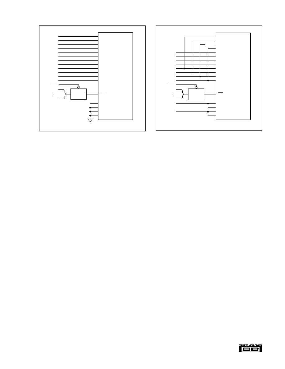
12- AND 16-BIT BUS INTERFACES
For operation with 12- and 16-bit buses, all four address
lines (A0 through A3) are connected to logic 0, and the latch
is enabled by CS asserted low. The DAC667 thus occupies
a single memory location.
This configuration uses the first and second rank registers
simultaneously. The CS input can be driven from an active-
low decoded address. It should be noted that any data bus
activity during the period when CS is low will cause activity
at the DAC667 output. If data is not guaranteed stable during
this period, the second rank register can be used to provide
double buffering. See Figure 12.
OUTPUT
DIGITAL
CONNECT
CONNECT
CONNECT
RANGE
INPUT CODES
PIN 9 TO
PIN 1 TO
PIN 2 TO
CONNECT PIN 4 TO
±
10V
Offset Binary
1
9
NC
6 (Through 50
fixed or 100
trim resistor.)
±
5V
Offset Binary
1 and 2
2 and 9
1 and 9
6 (Through 50
fixed or 100
trim resistor.)
±
2.5V
Offset Binary
2
3
9
6 (Through 50
fixed or 100
trim resistor.)
0 to +10V
Straight Binary
1 and 2
2 and 9
1 and 9
5 (Or optional trim. See Figure 7.)
0 to +5V
Straight Binary
2
3
9
5 (Or optional trim. See Figure 7.)
TABLE III. Output Voltage Range Connections.
FIGURE 10. Left-Justified 8-Bit Bus Interface.
DB11 (MSB)
DB10
DB9
DB8
DB7
DB6
DB5
DB4
DB3
DB2
DB1
DB0 (LSB)
D7
D6
D5
D4
D3
D2
D1
D0
WR
DAC667
Address
Decoder
A15
CS
A0
A1
A2
A3
A2
A1
A0
Whenever a 12-bit D/A is loaded from an 8-bit bus, two
bytes are required. If the software program considers the
data to be a 12-bit binary fraction (between 0 and 4095/
4096), the data is left-justified, with the eight most signifi-
cant bits in one byte and the remaining bits in the upper half
of another byte. Right-justified data calls for the eight least
significant bits to occupy one byte, with the four most
significant bits residing in the lower half of another byte,
simplifying integer arithmetic.
Figure 10 shows an addressing scheme for use with a DAC-
667 set up for left-justified data in an 8-bit system. The base
address is decoded from the high-order address bits and the
resultant active-low signal is applied to CS. The two LSBs
of the address bus are connected as shown to the DAC667
address inputs. The latches now reside in two consecutive
locations, with location X01 loading the four LSBs and
location X10 loading the eight MSBs and updating the output.
FIGURE 9. 12-Bit Data Formats for 8-Bit Systems.
DB7
(b) Right-Justified
DB6
DB5
DB4
DB3
DB2
DB1
DB0
X
X
X
X
DB11
DB10
DB9
DB8
DB3
(a) Left-Justified
DB2
DB1
DB0
X
X
X
X
DB11
DB10
DB9
DB8
DB7
DB6
DB5
DB4
9
Æ
DAC667
DB11 (MSB)
DB10
DB9
DB8
DB7
DB6
DB5
DB4
DB3
DB2
DB1
DB0 (LSB)
D11
D10
D9
D8
D7
D6
D5
D4
D3
D2
D1
D0
WR
DAC667
Address
Decoder
A15
CS
A0
A1
A2
A3
A0
FIGURE 12. Connections for 12- and 16-Bit Bus Interface.
FIGURE 11. Right-Justified 8-Bit Bus Interface.
DB11 (MSB)
DB10
DB9
DB8
DB7
DB6
DB5
DB4
DB3
DB2
DB1
DB0 (LSB)
D7
D6
D5
D4
D3
D2
D1
D0
WR
DAC667
Address
Decoder
A15
CS
A0
A1
A2
A3
A2
A1
A0