 | –≠–ª–µ–∫—Ç—Ä–æ–Ω–Ω—ã–π –∫–æ–º–ø–æ–Ω–µ–Ω—Ç: DAC729JH | –°–∫–∞—á–∞—Ç—å:  PDF PDF  ZIP ZIP |
©
1988 Burr-Brown Corporation
PDS-749C
Printed in U.S.A. October, 1993
Ultra-High Resolution
18-BIT DIGITAL-TO-ANALOG CONVERTER
FEATURES
q
16-BIT LINEARITY GUARANTEED
(K Grade)
q
USER ADJUSTABLE TO 18-BIT
LINEARITY
q
PRECISION INTERNAL REFERENCE
q
FAST SETTLING, LOW NOISE INTERNAL
OP AMP
q
LOW DRIFT
q
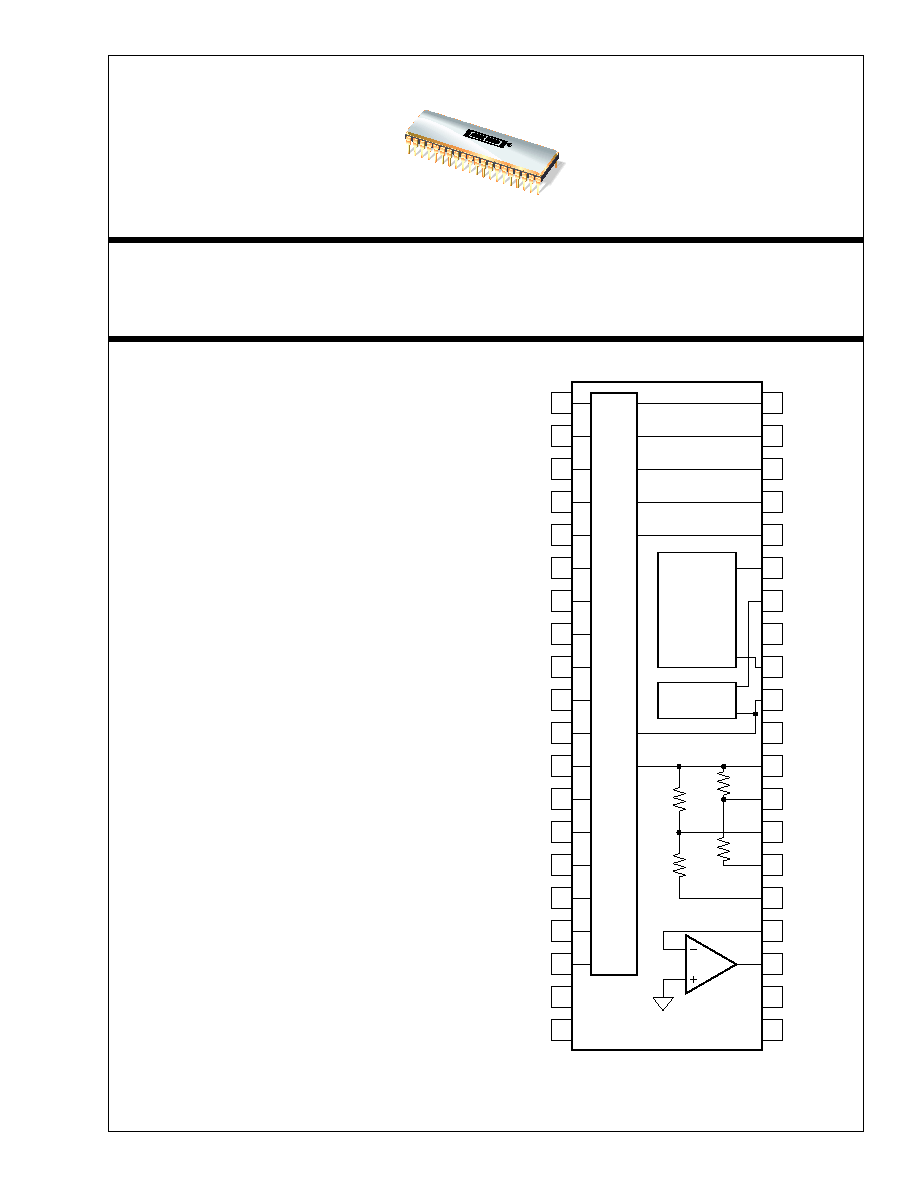
HERMETIC 40-PIN CERAMIC PACKAGE
q
I
OUT
OR V
OUT
OPERATION
DAC729
DESCRIPTION
The DAC729 sets the standard in very high accuracy
digital-to-analog conversion. It is supplied from the
factory at a guaranteed linearity of 16 bits, and is user-
adjustable to 18-bit linearity (1LSB = FSR/262144).
To attain this high level of accuracy, the design takes
advantage of Burr-Brown's thin-film monolithic DAC
process, dielectric op amp process, hybrid capabilities,
and advanced test and laser-trim techniques.
The DAC729 hybrid layout is specifically partitioned
to minimize the effects of external load-current-
induced thermal errors. The op amp design consists of
a fast settling precision op amp with a current buffer
within the feedback loop. This buffer isolates the load
from the precision op amp, which results in a fast
settling (8
µ
s to 16 bits) output. The standard 40-pin
package offers full hermeticity, contributing to the
excellent reliability of the DAC729.
18-Bit
I
OUT
DAC
1
2
3
4
5
6
7
8
9
10
11
12
13
14
15
16
17
18
19
20
5k
5k
5k
5k
40
39
38
37
36
35
34
33
32
31
30
29
28
27
26
25
24
23
22
21
Servo-Loop
Amplifier
Precision
10V
Reference
International Airport Industrial Park ∑ Mailing Address: PO Box 11400, Tucson, AZ 85734 ∑ Street Address: 6730 S. Tucson Blvd., Tucson, AZ 85706 ∑ Tel: (520) 746-1111 ∑ Twx: 910-952-1111
Internet: http://www.burr-brown.com/ ∑ FAXLine: (800) 548-6133 (US/Canada Only) ∑ Cable: BBRCORP ∑ Telex: 066-6491 ∑ FAX: (520) 889-1510 ∑ Immediate Product Info: (800) 548-6132
DAC729
DAC729
2
SPECIFICATIONS
ELECTRICAL
At T
A
= +25
∞
C, V
CC
=
±
15V, V
DD
= +5V, using internal reference op amp, unless otherwise noted. COB =
±
10V FSR, CSB = 0V to +10V FSR.
DAC729JH
DAC729KH
PARAMETER
MIN
TYP
MAX
MIN
TYP
MAX
UNITS
DIGITAL INPUT
Resolution
18
*
Bits
Digital Inputs
(1)
: V
IH
+2.4
+V
L
*
*
V
V
IL
0
+0.8
*
*
V
I
IH
, V
IN
= +2.7V
+5
*
µ
A
I
IL
, V
IN
= +0.4V
≠300
*
µ
A
TRANSFER CHARACTERISTICS
(2)
ACCURACY
Linearity Error
(3)
±
0.0015
±
0.00076
% of FSR
(4)
Differential Linearity Error
±
0.003
±
0.0015
% of FSR
Gain Error
(5)
±
0.05
±
0.10
*
*
%
Offset Error:
(5)
Voltage, COB
(6)
±
5
±
10
*
*
mV
CSB
(6)
±
3
±
5
*
*
mV
Current, COB
±
5
*
µ
A
CSB
±
1
*
µ
A
Power Supply Sensitivity, Unipolar:
±
15VDC
±
0.0001
±
0.0005
*
*
% of FSR/%V
S
+5VDC
±
0.0001
±
0.0005
*
*
% of FSR/%V
S
Bipolar Offset:
±
15VDC
±
0.0004
±
0.0015
*
*
% of FSR/%V
S
+5VDC
±
0.0001
±
0.0005
*
*
% of FSR/%V
S
Bipolar Gain:
±
15VDC
±
0.0005
±
0.0015
*
*
% of FSR/%V
S
+5VDC
±
0.0001
±
0.0005
*
*
% of FSR/%V
S
Output Noise (10Hz to 100kHz), Voltage: Bipolar Offset
29
*
µ
Vrms
Bipolar Gain
37
*
µ
Vrms
Current: Bipolar Offset
2.9
*
nArms
Bipolar Gain
3
*
nArms
Monotonicity (0
∞
C to +70
∞
C)
15
16
16
17
Bits
Differential Linearity Adjustment Resolution
(7)
18
*
Bits
DRIFT (Over Specification Temperature Range)
Gain Drift (Excluding Reference Drift)
±
3
±
5
*
*
ppm/
∞
C
Offset Drift (Excluding Reference Drift): COB (Bipolar)
±
2
±
5
*
*
ppm of FSR/
∞
C
CSB (Unipolar)
±
2
±
3
*
*
ppm of FSR/
∞
C
Linearity Error (at 0
∞
C and +70
∞
C)
±
0.3
±
1
±
0.3
±
0.5
ppm of FSR/
∞
C
Differential Linearity Error (at 0
∞
C and +70
∞
C)
±
0.5
±
2
±
0.5
±
1
ppm of FSR/
∞
C
STABILITY, LONG TERM (at +25
∞
C)
Gain (Exclusive of Reference)
±
5
±
5
ppm/1000hr
Offset: COB (Exclusive of Reference)
±
5
±
5
ppm of FSR/1000hr
CSB
±
5
±
5
ppm of FSR/1000hr
Linearity
±
2
±
2
ppm of FSR/1000hr
Reference
±
5
±
5
ppm/1000hr
OUTPUT
VOLTAGE OUTPUT MODE
Ranges: COB
±
2.5,
±
5,
±
10
*
V
CSB
0 to +10, 0 to +5
*
V
Output Current
±
5
*
mA
Output Impedance
0.15
*
Short Circuit Duration
Indefinite to Common
Indefinite to Common
CURRENT OUTPUT MODE
COB Ranges
±
1
*
mA
Output Impedance
2.86
*
k
CSB Ranges
0 to ≠2
*
mA
Output Impedance
4.0
*
k
Output Current Tolerance
±
0.1
*
% of FSR
Compliance Voltage
≠1 to +5
*
V
SETTLING TIME (To
±
0.00076% of FSR)
(8)
Voltage (Load = 2k
|| 100pF): Full-Scale Step
5
8
*
*
µ
s
1LSB Step (Major Carry)
(9)
4
7
*
*
µ
s
Slew Rate
20
*
V/
µ
s
Switching Transient Peak
500
*
mV
Switching Transient Energy
0.45
*
V-
µ
s
Current Full-Scale Step (2mA
X
10
|| 1pF)
300
*
ns

DAC729
3
SPECIFICATIONS
(CONT)
ELECTRICAL
At T
A
= +25
∞
C, V
CC
=
±
15V, V
DD
= +5V, using internal reference op amp, unless otherwise noted. COB =
±
10V FSR, CSB = 0V to +10V FSR.
* Specifications same as DAC729JH.
NOTES: (1) TTL- and CMOS-compatible. (2) Specified for V
OUT
mode using the internal op amp. (3)
±
0.00076% of full-scale range is 1/2LSB for 16-bit resolution. (4)
FSR means full-scale range, 20V for
±
10V range, etc. (5) Adjustable to zero error with an external potentiometer. (6) COB is complementary offset binary (bipolar); CSB
is complementary straight binary (unipolar). (7) Using the MSB adjustment circuit, the user may improve the DAC linearity to 1/2LSB of this specification with gain and
offset errors adjusted to zero at 25
∞
C. (8) Maximum represents 3
limit, not 100% production tested. (9) At the major carry; 20000 to 1FFFF
HEX
and from 1FFFF to
20000
HEX
. (10) Maximum with no degradation in specifications. External loads must be constant.
DAC729JH
DAC729KH
PARAMETER
MIN
TYP
MAX
MIN
TYP
MAX
UNITS
REFERENCE
Output (pin 32) :Voltage
+9.990
+10.000
+10.010
*
*
*
V
Source Current
(10)
+4
*
mA
Temperature Coefficient
±
2
±
4
*
*
ppm/
∞
C
Short-Circuit Duration
Indefinite to Common
Indefinite to Common
Power Supply Sensitivity
0.00025
0.003
*
*
%/V
POWER SUPPLY REQUIREMENTS
Voltage: +V
CC
+13.5
+15
+16.5
*
*
*
V
≠V
CC
≠16.5
≠15
≠13.5
*
*
*
V
V
DD
+4.75
+5
+5.25
*
*
*
V
Current: +V
CC
+30
+40
*
*
mA
≠V
CC
≠45
≠60
*
*
mA
V
DD
+18
+25
*
*
mA
Power Dissipation (Rated Supplies)
1.22
1.63
*
*
W
ENVIRONMENTAL SPECIFICATIONS
Temperature Range: Specification
0
+70
*
*
∞
C
Storage
≠60
+150
*
*
∞
C
V
DD
to Common ........................................................................ 0V to +7V
+V
CC
to Common .................................................................... 0V to +18V
≠V
CC
to Common .................................................................... 0V to ≠18V
Digital Data Inputs (pins 1-18) to Common ............................ ≠0.5V to V
DD
Reference Voltage In (pin 31) ................................................ +9V to +11V
Reference Out (pin 32) to Common ............... Indefinite Short to Common
External Voltage Applied to D/A Output (pin 29) ..................... ≠5V to +5V
External Voltage Applied to Feedback Resistors
(pins 25, 26, 27, 28) .......................................................... ≠15V to +15V
V
OUT
(pin 23) ................................................... Indefinite Short to Common
Power Dissipation ........................................................................ 3000mW
Storage Temperature ...................................................... ≠60
∞
C to +150
∞
C
Lead Temperature (soldering, 10s) ............................................... +300
∞
C
NOTE: (1) Stresses above those listed under "Absolute Maximum Ratings" may
cause permanent damage to the device. Exposure to absolute maximum
conditions for extended periods may affect device reliability.
ABSOLUTE MAXIMUM RATINGS
(1)
ORDERING INFORMATION
PRODUCT
PACKAGE
TEMPERATURE RANGE
DAC729JH
40-Pin Hermetic DIP
0
∞
C to +70
∞
C
DAC729KH
40-Pin Hermetic DIP
0
∞
C to +70
∞
C
DAC729KH-BI
40-Pin Hermetic DIP
0
∞
C to +70
∞
C
PACKAGE INFORMATION
PACKAGE DRAWING
PRODUCT
PACKAGE
NUMBER
(1)
DAC729JH
40-Pin Hermetic DIP
214
DAC729KH
40-Pin Hermetic DIP
214
DAC729KH-BI
40-Pin Hermetic DIP
214
NOTE: (1) For detailed drawing and dimension table, please see end of data
sheet, or Appendix C of Burr-Brown IC Data Book.
The information provided herein is believed to be reliable; however, BURR-BROWN assumes no responsibility for inaccuracies or omissions. BURR-BROWN
assumes no responsibility for the use of this information, and all use of such information shall be entirely at the user's own risk. Prices and specifications are subject
to change without notice. No patent rights or licenses to any of the circuits described herein are implied or granted to any third party. BURR-BROWN does not
authorize or warrant any BURR-BROWN product for use in life support devices and/or systems.
DAC729
4
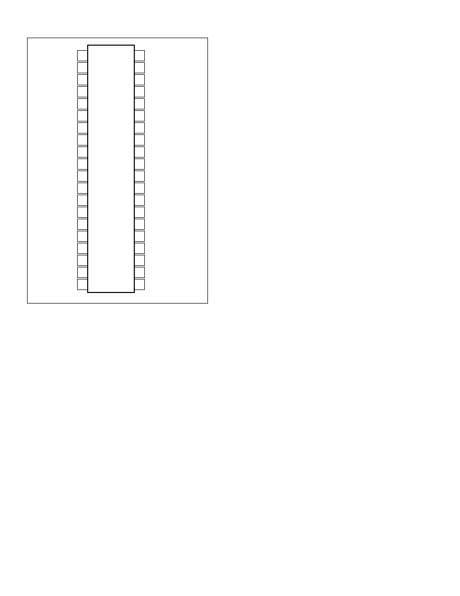
PIN CONNECTIONS
(MSB) Bit 1
Bit 2
Bit 3
Bit 4
Bit 5
Bit 6
Bit 7
Bit 8
Bit 9
Bit 10
Bit 11
Bit 12
Bit 13
Bit 14
Bit 15
Bit 16
Bit 17
(LSB) Bit 18
V
DD
(5V)
Digital Common
V
POT
Bit 1 Adjust
Bit 2 Adjust
Bit 3 Adjust
Bit 4 Adjust
Reference Adjust
Gain Adjust
Reference Common
Reference Out
Reference In
Analog Common
I
OUT
5k
Feedback
5k
Feedback
10k
Feedback
10k
Feedback
Summing Junction
V
OUT
+V
CC
(15V)
≠V
CC
(15V)
1
2
3
4
5
6
7
8
9
10
11
12
13
14
15
16
17
18
19
20
40
39
38
37
36
35
34
33
32
31
30
29
28
27
26
25
24
23
22
21
Top View
DIP

DAC729
5
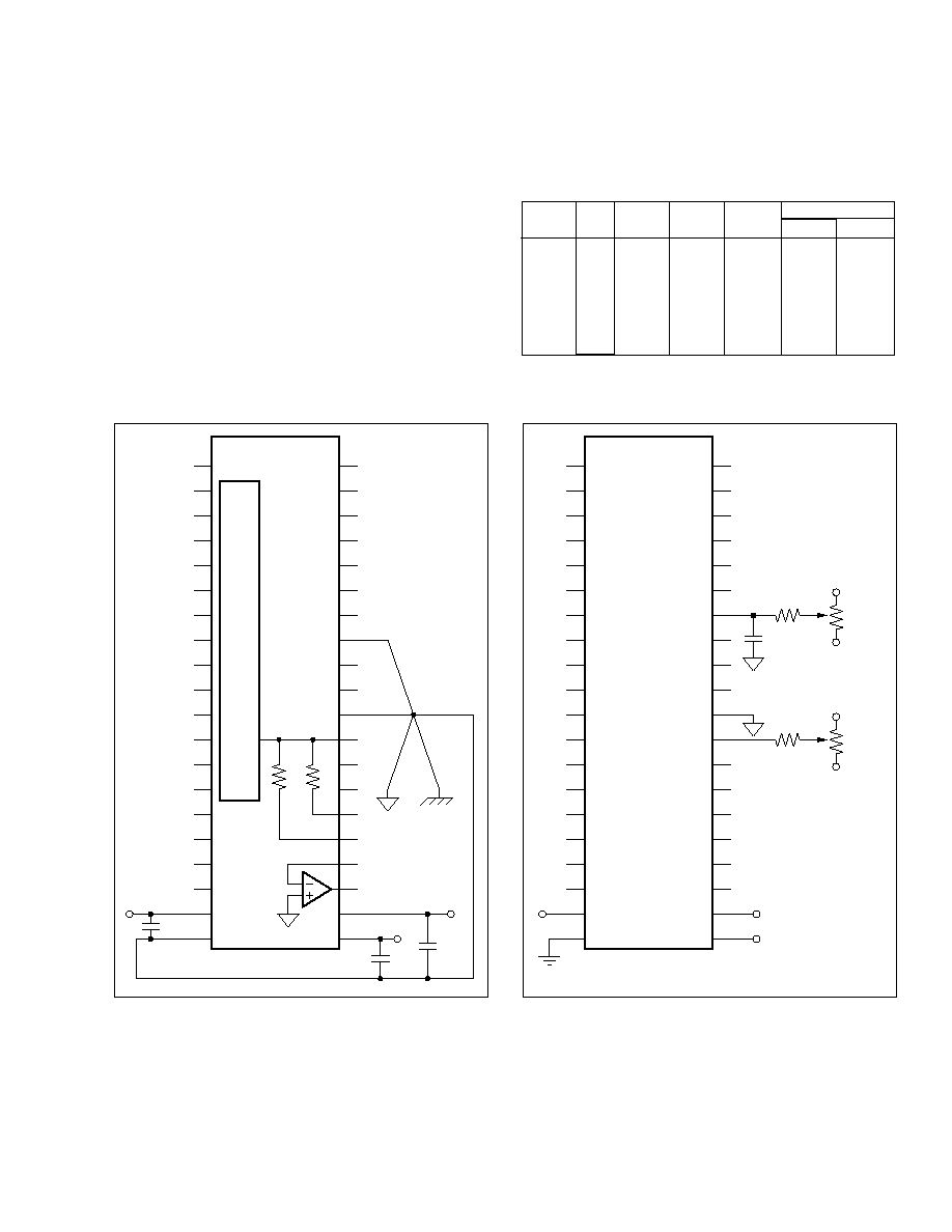
THEORY OF OPERATION
The DAC729 is an 18-bit digital-to-analog converter sys-
tem, including a precision reference, low noise, fast settling
operational amplifier, and an 18-bit current source/DAC
chip contained in a hermetic 40-pin ceramic dual-in-line
package. Refer to Figure 11 for a schematic diagram of the
DAC729.
THE INTERNAL REFERENCE
The reference consists of a very low temperature coefficient
closed-loop reference zener circuit that has been tempera-
ture-drift-compensated by laser-trimming a zener current to
achieve less than 1ppm/
∞
C temperature drift of V
REF
.
By strapping pin 32 (Reference Out) to pin 31 (Reference
In), the DAC will be properly biased from the internal
reference. The internal reference may be fine adjusted using
pin 35 as shown in Figure 7. The reference has an output
buffer that will supply 4mA for use external to the DAC729.
This load must remain constant because changing load on
the reference may change the reference current to the DAC.
In systems where several components need to track the same
system reference, the DAC729 may be used with an external
10V reference, however, the internal reference has lower
noise (6
µ
Vp-p) and better stability than other references
available.
THE OPERATIONAL AMPLIFIER
To support a DAC of this accuracy, the operational amplifier
must have a maximum gain-induced error of less than
1/3LSB, independent of output swing (the op amp must be
linear!) To support 15 bits (1/2-bit linearity), the op amp
must have a gain of 130,000V/V. For 18 bits, the minimum
DAC ANALOG OUTPUT
DIGITAL INPUT
COB
20V FSR
CSB
10V FSR
00 0000 0000 0000 0000 + Full Scale 9.999924V + Full Scale 9.999962V
11 1111 1111 1111 1111 ≠ Full Scale
≠10V
≠ Full Scale
0V
TABLE I. Digital Input Coding.
BURN-IN SCREENING
Burn-in screening is an option available for the DAC729
family of products. Burn-in duration is 160 hours at 100
∞
C
(or equivalent combination of time and temperature).
All units are tested after burn-in to ensure that grade speci-
fications are met.
gain is well over 500,000V/V. Since thermal feedback is the
major limitation of gain for mono op amps, the amplifier
was designed as a high gain, fast settling mono op amp,
followed by a monolithic, unity-gain current buffer to isolate
the thermal effects of external loads from the input stage
gain transistors. The op amp and buffer are separated from
the DAC chip, minimizing thermally-induced linearity er-
rors in the DAC circuit. The op amp, like the reference, is
not dedicated to the DAC729. The user may want to add a
network, or select a different amplifier. The DAC729 inter-
nal op amp is intended to be the best choice for accuracy,
settling time, and noise.
THE DAC CHIP
The heart of the DAC729 is a monolithic current source and
switch integrated circuit. The absolute linearity, differential
linearity, and the temperature performance of the DAC729
are the result of the design, which utilizes the excellent
element matching of the current sources and switch transis-
tors to each other, and the tracking of the current setting
resistors to the feed back resistors. Older discrete designs
cannot achieve the performance of this monolithic DAC
design.
The two most significant bits are binarily weighted inter-
digitated current sources. The currents for bits 3 through 18
are scaled with both current source weighting and an R-2R
ladder. The circuit design is optimized for low noise and low
superposition error, with the current sources arranged to
minimize both code-dependent thermal errors and IR drop
errors. As a result, the superposition errors are typically less
than 20
µ
V.
The DAC chip is biased from a servo amplifier feeding into
the base line of the current sources. This servo amplifier sets
the collector current to be mirrored and scaled in the DAC
chip current sources, as shown in Figure 11. The reference
current for the servo is established by the reference voltage
applied to pin 31 feeding an internal resistor (20k
) to the
virtual ground of the servo amplifier.
DISCUSSION
OF SPECIFICATIONS
DIGITAL INPUT CODES
The DAC729 accepts complementary digital input codes in
either binary format (CSB for Unipolar or COB for Bipolar;
see Table I).
ELECTROSTATIC
DISCHARGE SENSITIVITY
Any integral circuit can be damaged by ESD. Burr-Brown
recommends that all integrated circuits be handled with
appropriate precautions. Failure to observe proper handling
and installation procedures can cause damage.
ESD damage can range from subtle performance degrada-
tion to complete device failure. Precision integrated circuits
may be more susceptible to damage because very small
parametric changes could cause the device not to meet
published specifications.

DAC729
6
ACCURACY
Linearity
This specification describes one of the most important mea-
sures of performance of a D/A converter. Linearity error is
the deviation of the analog output versus code transfer
function from a straight line drawn through the end points
(all bits ON point and all bits OFF point).
Differential Linearity Error
Differential Linearity Error (DLE) of a D/A converter is the
deviation from an ideal 1LSB change in the output from one
adjacent output state to the next. A differential linearity error
specification of
±
1/2LSB means that the output step sizes
can be between 1/2 LSB and 3/2LSB when the input changes
from one adjacent input state to the next. A negative DLE
specification of no more than ≠1LSB (≠0.0015% for 16-bit
resolution) insures monotonicity to 16 bits.
Monotonicity
Monotonicity assures that the analog output will increase or
remain the same for increasing input digital codes. The
DAC729KH is specified to be monotonic to 16 bits over the
entire specification temperature range.
DRIFT
Gain Drift
Gain drift is a measure of the change in the full-scale range
output over temperature expressed in parts per million per
degree centigrade (ppm/
∞
C). Gain drift is measured by: (1)
testing the end point differences for each D/A at t
MIN
, +25
∞
C,
and t
MAX
; (2) calculating the gain error with respect to the
+25
∞
C value; and (3) dividing by the temperature change.
Offset Drift
Offset drift is a measure of the change in the output with
3FFFF
H
applied to the digital inputs over the specified
temperature range. The maximum change in offset at t
MIN
or
t
MAX
is referenced to the offset error at +25
∞
C and is divided
by the temperature change. This drift is expressed in parts
per million of full-scale range per degree centigrade (ppm of
FSR/
∞
C).
SETTLING TIME
Settling time of the D/A is the total time required for the
analog output to settle within an error band around its final
value after a change in digital input. Settling time includes
the slew time of the op amp.
Voltage Output
Settling times are specified to
±
0.00076% of FSR scale
range change of 20V (COB) or 10V (CSB) and a 1LSB
change at the "major carry," the point at which the worst-
case settling time occurs. (This is the worst-case point since
all of the input bits change when going from one code to the
next.)
Current Output
Settling times are specified to
±
0.00076% of FSR for a full-
scale range change with an output load resistance of 10
.
COMPLIANCE VOLTAGE
Compliance voltage applies only to the current output mode
of operation. It is the maximum voltage swing allowed on
the output current pin while still being able to maintain
specified linearity.
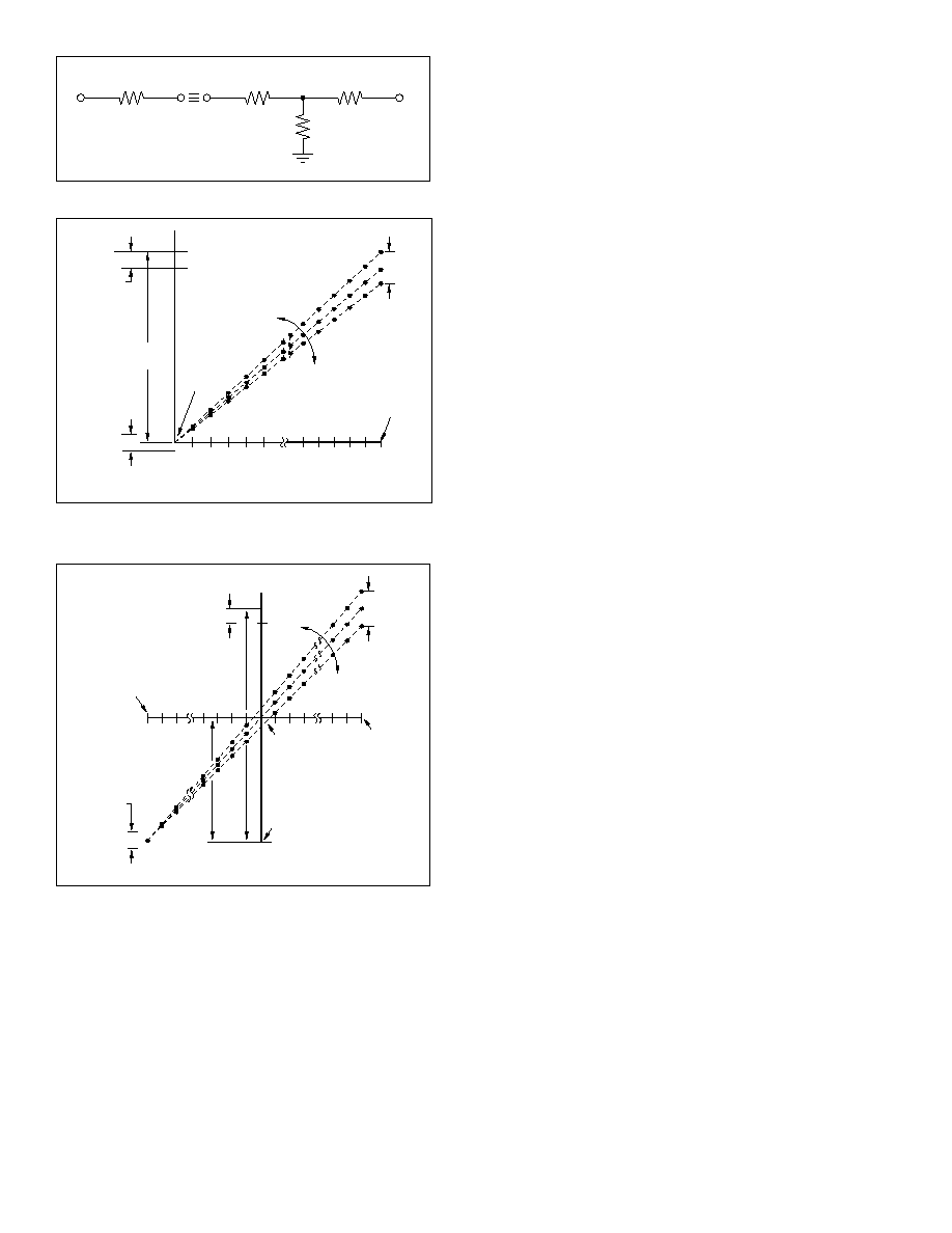
POWER SUPPLY SENSITIVITY
Power supply sensitivity is a measure of the effect of a
change in a power supply voltage on the D/A converter full-
scale output. It is defined as a percent of FSR change in the
output per percent of change in either the positive supply
(+V
CC
), negative supply (≠V
CC
), or logic supply (V
DD
) about
the nominal power supply voltages (see Figure 1). It is
specified for DC or low frequency changes. The typical
performance curve in Figure 1 shows the effect of high
frequency changes in power supply voltages using internal
reference, DAC, and op amp.
FIGURE 1. Power Supply Sensitivity vs Frequency Using
Internal Reference and Op Amp.
OPERATING INSTRUCTIONS
POWER SUPPLY CONNECTIONS
For optimum performance and noise rejection, power supply
decoupling capacitors should be added as shown in Figure 2.
These capacitors (1
µ
F to 10
µ
F tantalum recommended)
should be located at the DAC729.
EXTERNAL OFFSET AND GAIN ADJUSTMENT
Offset and gain may be trimmed by installing external offset
and gain potentiometers. Connect these potentiometers as
shown in Figure 3 and adjust as described below. TCR of
the potentiometers should be 100ppm/
∞
C or less. The 3.9M
and 510k
resistors (20% carbon or better) should be
located close to the DAC729 to prevent noise pickup. If it
is not convenient to use these high-value resistors, an
equivalent "T" network, as shown in Figure 4, may be
substituted in place of the 3.9M
. A 0.001
µ
F to 0.01
µ
F
capacitor should be connected from Gain Adjust (pin 34) to
DAC729
7
common to shunt noise pickup. This capacitor should be a
low leakage film type (such as MylarTM or TeflonTM).
Refer to Figures 5 and 6 for relationship of offset and gain
adjustments to unipolar and bipolar D/A converters.
OFFSET ADJUSTMENT
For unipolar (CSB) configurations, apply the digital input
code that should produce zero potential output and adjust the
offset potentiometer for zero output.
For bipolar (COB) configurations, apply the digital input
code that should produce the maximum negative output
voltage. See Table II for corresponding codes and Figures 2
and 3 for offset adjustment connections. Offset adjust should
be made prior to gain adjust.
GAIN ADJUSTMENT
For either unipolar or bipolar configurations, apply the
digital input that should give the maximum positive output
voltage. Adjust the gain potentiometer for this positive full-
scale voltage. See Table II for positive full-scale voltages
and Figure 3 for gain adjustment connections.
OUTPUT
CONNECT CONNECT CONNECT
RANGE
CODE
PIN 23
PIN 31
PIN 24
16-BITS
18-BITS
±
10V
COB
to Pin 25
to Pin 26
to Pin 29
9.9969V
9.99992V
±
5V
COB
to Pin 27
to Pin 26
to Pin 29
4.9998V
9.99996V
±
2.5V
COB
to Pin 27
to Pin 26
to Pins
2.4992V
2.49998V
29 & 25
0 to 10V
CSB
to Pins
N/C
to Pin 29
9.9998V
9.99996V
25 & 26
0 to 5V
CSB
to Pins
N/C
to Pin 29
4.9999V
4.99998V
27 & 28
GAIN ADJUST
TABLE II. Output Range Connections and Gain Adjust
Voltage.
Mylar
TM
, Teflon
TM
E.I. du Pont de Nemours & Co.
1
2
3
4
5
6
7
8
9
10
11
12
13
14
15
16
17
18
19
20
40
39
38
37
36
35
34
33
32
31
30
29
28
27
26
25
24
23
22
21
+
1µF
+
1µF
+
1µF
≠15V
+15V
+5V V
LOGIC
10k
Analog
Common
Reference Common
Digital Common
10k
18-Bit
DAC
FIGURE 2. Ground Connections and Supply Bypass.
≠V
CC
Offset Adjust
1
2
3
4
5
6
7
8
9
10
11
12
13
14
15
16
17
18
19
20
40
39
38
37
36
35
34
33
32
31
30
29
28
27
26
25
24
23
22
21
≠V
CC
= 15V
+5V
0.0022µF
270k
+V
CC
= 15V
NOTE: (1) Mylar
TM
or Teflon
TM
Film.
3.9M
≠V
CC
Gain Adjust
+V
CC
10k
to
100k
10k
to
100k
+V
CC
(1)
FIGURE 3. Gain and Offset Adjust Hook-Up.
DAC729
8
much more critical as the accuracy of the system increases.
The DAC729 has been designed to minimize these applica-
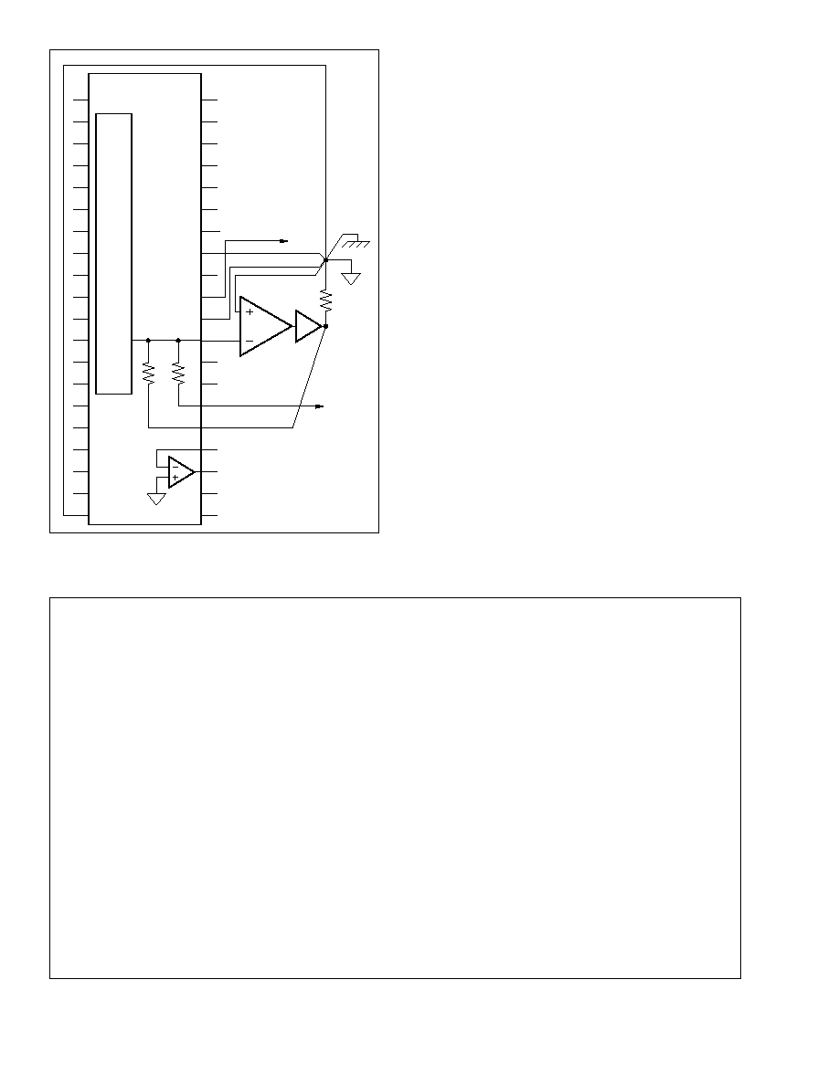
tions problems to a large degree. The basics of "Kelvin
sensing" and "holy point" grounding will be the most impor-
tant considerations in optimizing the absolute accuracy of
the system. Figure 9 shows the proper connection of the
DAC with the holy-point ground and the Kelvin-sensed-
output connection at the load.
The DAC729 has three separate supply common (ground)
pins. Reference common (pin 33) carries the return current
from the internal reference and the output I/V converter
common. The current in pin 33 is stable and independent of
code or load. Digital common (pin 20) carries the variable
currents of the biasing circuits. Analog common (pin 30) is
the termination of the R-2R ladder and also carries the
"waste current" from the off side of the current switches.
These three ground pins must be star connected to system
ground for the DAC to bias properly and accurately. Good
ground connections are essential, because an IR drop of just
39
µ
V completely swamps out a 10V FSR 18-bit LSB.
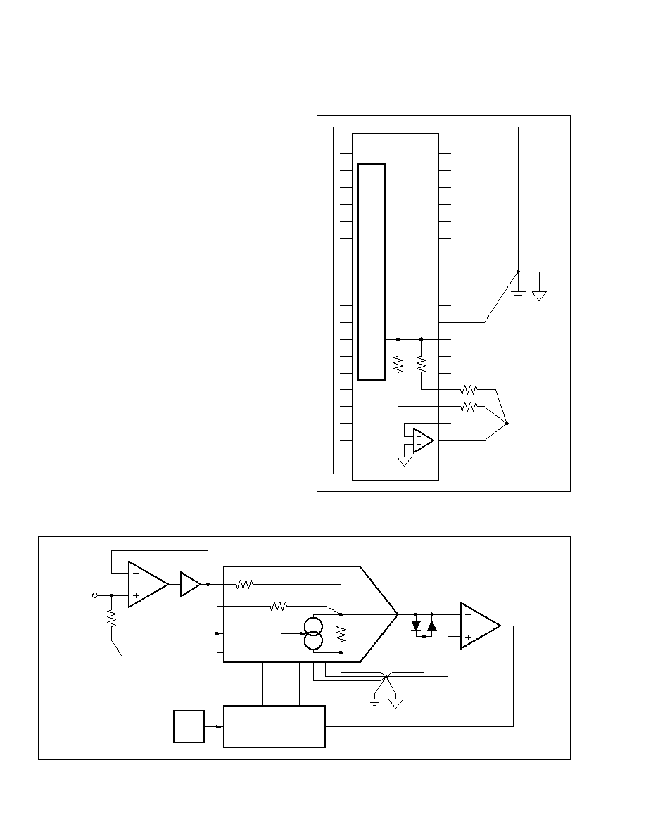
When the application is such that the DAC must control
loads of greater than
±
5mA with rated accuracy, it is recom-
mended that an external op amp or op amp buffer combina-
tion be used to dissipate the variable power external to the
DAC729. This minimizes the temperature variations on the
precision D/A converter. Figure 10 illustrates a method of
connecting the external amplifier for
±
10V operation, while
using an external reference.
When driving loads to greater than
±
10V, care must be taken
that the internal resistors are never exposed to greater than
±
10V, and that the summing junction is clamped to insure
that the voltage never exceeds
±
5V. Clamping the summing
junction with diodes (parallel opposing connection) to ground
will give the best transient response and settling times.
TRUE 18-BIT PERFORMANCE
(Differential Linearity Adjustment)
To take full advantage of the DAC729's accuracy, the four
MSBs have adjustment capabilities. A simplified schematic
(Figure 11) shows the internal structure of the DAC current
source and the adjustment input terminal. The suggested
network for adjusting the linearity is shown in Figure 12.
This circuit has nearly twice the range that is required for the
DAC729JH. The range is intentionally narrow so as to
minimize the effect of temperature drift or stability problems
in the potentiometers. The potentiometers are biased in an
identical fashion to the internal DAC current sources to
minimize power supply sensitivity and drift over tempera-
ture. Low leakage capacitors such as Mylar or Teflon film
are essential.
The linearity adjustment requires a digital voltmeter with 7
digits of resolution on the 10V range (1
µ
V resolution) and
excellent linearity. For the DAC, 1LSB of the 0V to 10V
scale (10 FSR) is 38
µ
V. To be 1/2LSB linear, the measure-
ment must resolve 19
µ
V. The meter must be properly
calibrated and linear to 1ppm of range.
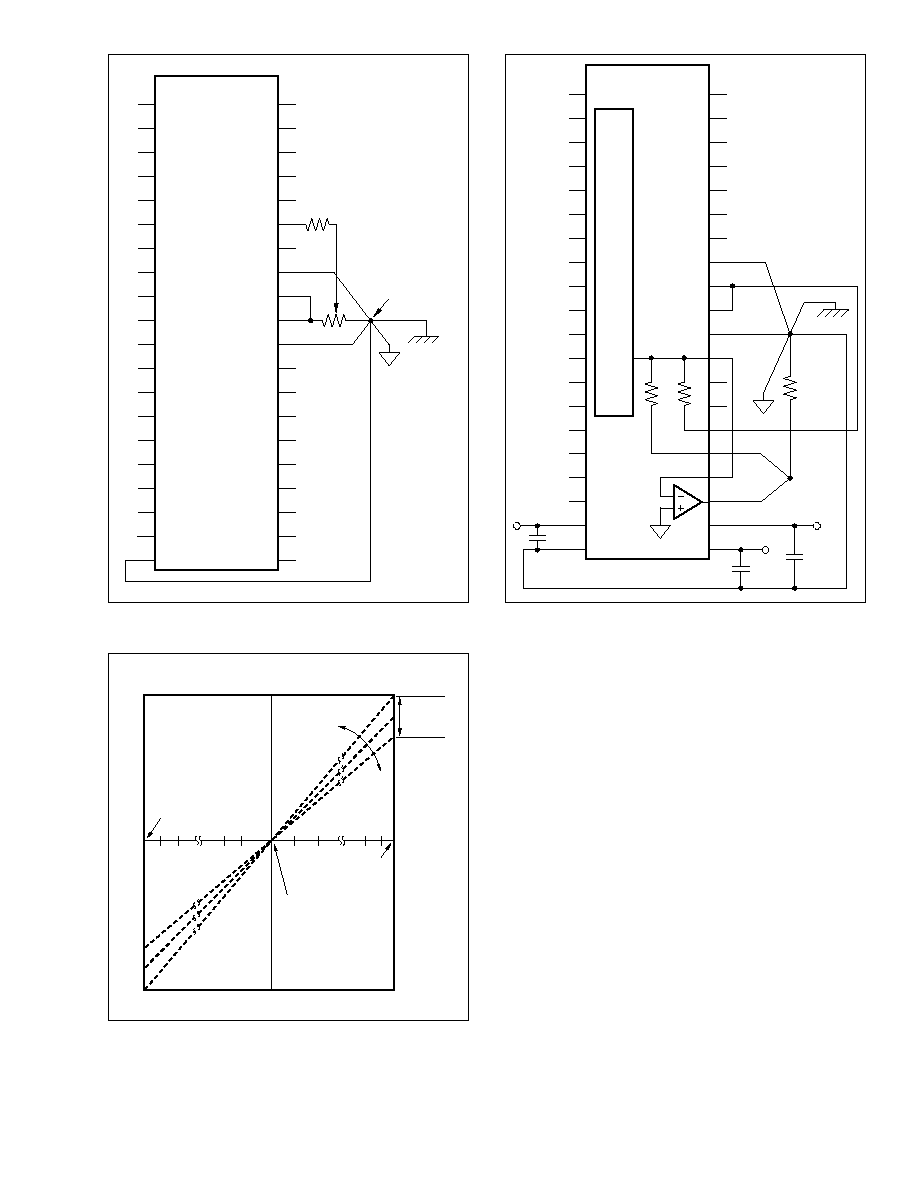
FIGURE 5. Relationship of Offset and Gain Adjustments for
a Unipolar D/A Converter.
FIGURE 6. Relationship of Offset and Gain Adjustments for
a Bipolar D/A Converter.
REFERENCE ADJUSTMENT
The internal reference may be fine adjusted using pin 35 as
shown in Figure 7. Adjusting the reference has a similar
effect on the DAC as gain adjust, except the transfer charac-
teristic rotates around bipolar zero for a bipolar connection
as shown in Figure 8.
LAYOUT/APPLICATIONS SUGGESTIONS
Obviously, the management of IR drops, power supply
noise, thermal stability, and environmental noise becomes
FIGURE 4. Equivalent Resistances.
180k
180k
3.9M
10k
1LSB
Full Scale
Range
Analog Output
Digital Input
Gain Adjustment
Rotates the Line
Range of
Gain Adj.
Input =
00000
H
Offset Adj.
Translates
the Line
Input =
3FFFF
H
+ Full
Scale
MSB on,
All Others Off
Range of
Gain Adj.
1LSB
Bipolar V
Offset
Analog Output
Digital Input
Input =
00000
H
Offset Adj.
Translates
the Line
Input =
3FFFF
H
+ Full Scale
Full Scale
Range
Gain Adjustment
Rotates the Line
Range of
Offset Adj.
≠Full Scale
DAC729
9
FIGURE 9. Typical Hook-Up Diagram with "Holy Point"
Ground and Kelvin Sense Load, Using Internal
Op Amp and Reference.
1
2
3
4
5
6
7
8
9
10
11
12
13
14
15
16
17
18
19
20
40
39
38
37
36
35
34
33
32
31
30
29
28
27
26
25
24
23
22
21
+
1µF
+
1µF
+
1µF
≠15V
+15V
+5V V
DD
10k
Common
Digital Common
10k
18-Bit
DAC
R
L
Analog
Common
I
OUT
Ref. Out
Ref. In
With the DAC connected for 0 to 10V output (Figure 13),
the adjustment procedure is to set the DAC code and mea-
sure as follows:
FOURTH MSB ADJUSTMENT (Pin 36)
1. Set Code = 11 1100 0000 0000 0000
2. Measure V
OUT
3. Set Code = 11 1011 1111 1111 1111
4. Measure V
OUT
and record the difference.
5. Adjust 4th MSB potentiometer to make difference +38
µ
V.
6. Repeat steps 1 through 5 to confirm.
THIRD MSB ADJUSTMENT (Pin 37)
1. Set Code = 11 1000 0000 0000 0000
2. Measure V
OUT
3. Set Code = 11 0111 1111 1111 1111
4. Measure V
OUT
and record the difference.
5. Adjust 3rd MSB potentiometer to make difference +38
µ
V.
6. Repeat steps 1 through 5 to confirm.
FIGURE 7. V
REF
Adjust.
R
S
1M
20k
1
2
3
4
5
6
7
8
9
10
11
12
13
14
15
16
17
18
19
20
40
39
38
37
36
35
34
33
32
31
30
29
28
27
26
25
24
23
22
21
Holy Point
Ground Connection
R
S
= 1M
Gives 20mV
Adjustment Range
Ref. Adj.
Ref. Out
Ref. In
FIGURE 8. Effect of V
REF
Adjust on a COB Connected
DAC729.
00000
H
Input = 3FFFF
H
MSB On,
All Others Off 2FFFF
H
Range of
Gain Adjust
Analog Output
Digital Input
Offset Adjust
Translates
the Line
+ Full Scale
Gain Adjust
Rotates
the Line
≠ Full Scale
DAC729
10
FIGURE 10. Using an External Op Amp with Buffer and
External Reference for
±
10V Output.
1
2
3
4
5
6
7
8
9
10
11
12
13
14
15
16
17
18
19
20
40
39
38
37
36
35
34
33
32
31
30
29
28
27
26
25
24
23
22
21
10k
10k
18-Bit
DAC
From System
Reference
R
L
From System
Reference
OPA633
OPA602
Ref. In
SECOND MSB ADJUSTMENT (Pin 38)
1. Set Code = 11 0000 0000 0000 0000
2. Measure V
OUT
3. Set Code = 10 1111 1111 1111 1111
4. Measure V
OUT
and record the difference.
5. Adjust 2nd MSB potentiometer to make difference +38
µ
V.
6. Repeat steps 1 through 5 to confirm.
MSB ADJUSTMENT (Pin 39)
1. Set Code = 10 0000 0000 0000 0000
2. Measure V
OUT
3. Set Code = 01 1111 1111 1111 1111
4. Measure V
OUT
and record the difference.
5. Adjust the MSB potentiometer to make difference +38
µ
V.
6. Repeat steps 1 through 5 to confirm.
APPLICATIONS
The DAC729 is the DAC of choice for applications requir-
ing very high resolution, accuracy, and wide dynamic range.
DIGITAL AUDIO
The excellent linearity and differential linearity are ideal for
PCM professional audio and waveform generation applica-
tions.
FIGURE 11. DAC729 Simplified Schematic.

DAC729
11
FIGURE 12. Differential Linearity Adjustment Circuit for the
4MSBs.
FIGURE 13. 0 to 10V FSR.
1
2
3
4
5
6
7
8
9
10
11
12
13
14
15
16
17
18
19
20
40
39
38
37
36
35
34
33
32
31
30
29
28
27
26
25
24
23
22
21
10k
10k
18-Bit
DAC
V
OUT
The DAC729 offers superb dynamic range. Dynamic range
is a measure of the ratio of the smallest signals the converter
can produce to the full-scale range, usually expressed in
decibels (dB). The theoretical dynamic range of a converter
is approximately 6dB per bit. For the DAC729 the theoreti-
cal range is 108dB! The actual dynamic range is limited by
noise (signal-to-noise) and linearity errors. The DAC729's
6
µ
V typical noise floor, fast settling op amp, and adjustable
18-bit linearity minimize the limitation.
Total harmonic distortion (THD) is the measure of the
magnitude and distribution of the linearity error, differential
linearity error, noise, and quantization error. The THD is
defined as the ratio of the square root of the sum of the
squares of the harmonics to the values of the input funda-
mental frequency. The rms value of a DAC error can be
shown to be
where n is the number of samples in one cycle of any given
sine wave, E
L
(i) is the linearity error of the DAC729 at each
sampling point, and E
Q
(i) is the quantization error at each
sampling point. The THD can then be expressed as
where E rms is the rms signal-voltage level.
This expression indicates that, in general, there is a correla-
tion between the THD and the square root of the sum of the
squares of the linearity errors at each digital word of interest.
However, this expression does not mean that the worst-case
linearity error of the D/A is directly correlated to the THD.
The DAC729 has demonstrated THD of 0.0009% at full
scale (at 1kHz). This is the level of distortion that is desired
to test other professional audio products, making the DAC729
ideal for professional audio test equipment.
The ability to adjust the linearity of the 4MSBs, the 18-bit
resolution, fast settling and low noise give the DAC729
unmatched performance.
AUTOMATIC TEST EQUIPMENT
The pin functions of the DAC729 are convenient for use in
automatic test equipment systems. The ability to use internal
or external reference and internal or external op amp means
versatility for the system designer. For example, in auto-
matic test systems with several DACs and ADCs, it is
desirable to operate all of the high accuracy converters from
the same reference, improving the tracking characteristics of
those components to one another. The reference in the
DAC729 is a very stable precision reference, and is suitable
for use as the system reference.
Test systems, and other large systems are the ideal applica-
tion for a DAC of this accuracy, because the DAC will be
calibrated in the environment in which it will be used. Since
the environment is very stable, the manual calibration (Fig-
ure 12) may be adequate. However, highly automated sys-
tems will go to an automatic calibration routine. Replacing
n
1
RMS
=
[E
L
(i) + E
Q
(i)]
2
i =1
n
1.0M
100k
0.01µF
(1)
36
≠V
CC
1.0M
100k
0.01µF
(1)
37
≠V
CC
1.0M
100k
0.01µF
(1)
38
≠V
CC
1.0M
Bit 1
Adjust
100k
0.01µF
(1)
39
V
POT
40
≠V
CC
21
≠V
CC
150k
150k
150k
150k
NOTE: (1) Low leakage film type.
Bit 2
Adjust
Bit 3
Adjust
Bit 4
Adjust
THD = = X
x
100%
E
RMS
RMS
E
RMS
i =1
n
1
n
[E
L
(i) + E
Q
(i)]
2
(2)
DAC729
12
the potentiometers in Figure 12 with V
OUT
DACs, and using
sample and difference measurements, the major carry bit
weights can be measured, and external DACs used to adjust
the differential linearity of the DAC729. A successive ap-
proximation routine yields the fastest calibration. The output
voltage of the external DACs will have to be level shifted,
as the bit adjustment potentiometer must be able to achieve
≠V
CC
to give the full adjust range.
Because the DAC729 feedback resistors have a tolerance of
±
0.1%, the output range can be rescaled slightly with small-
value fixed external resistors to give convenient ranges. A
popular range is 0V to +10.24V which gives even 5mV steps
at 11 bits. In this case, the LSB size is 39.06
µ
V. Figure 14
shows how to connect two 240
resistors in series with the
internal 10k
resistors to give a 0V to 10.24V full-scale
range. Another convenient range might be 0V to +10.48576V
which gives an even 40
µ
V LSB step size.
THE HEART OF AN 18-BIT ADC
The DAC729 makes a good building block in ADC applica-
tions. The key to ADC accuracy is differential linearity of
the DAC. The ability to adjust to 18-bit linearity, coupled
with the fast settling time of the DAC729 makes the design
cycle for an 18-bit successive approximation ADC much
faster, and the production more consistent. Figure 15 shows
the DAC as the heart of a successive approximation ADC.
The clock and successive approximation register could be
implemented in 7400 series TTL, as a simple gate-array or
standard cell, or part of a local processor.
With the DAC out of the way, the comparator is the toughest
part of the ADC design. To resolve an 18-bit LSB, and
interface to a TTL-logic device, the comparator must have a
gain of 500kV/V (5
X
actual) as well as low hysteresis, low
noise, and low thermally induced offsets. With this much
gain, a slow comparator may be desired to reduce the risk of
instability.
FIGURE 15. Block Diagram of an 18-Bit Resolution
±
10V
IN
ADC.
FIGURE 14. 0V to 10.24V Using Internal Op Amp and
Internal Reference.
OPA602
10M
To Holy
Point Ground
OPA633
10k
10k
Ref In
Ref Out
Clock
SAR
2k
Custom Design
Comparator
DAC729
18-Bits
The feedback resistors of the DAC are the input scaling
resistors of the ADC. An OPA602 and an OPA633 make an
excellent buffer for the input signal, giving a very high input
impedance to the signal (minimizing IR drop) while main-
taining the linearity.
1
2
3
4
5
6
7
8
9
10
11
12
13
14
15
16
17
18
19
20
40
39
38
37
36
35
34
33
32
31
30
29
28
27
26
25
24
23
22
21
10k
10k
18-Bit
DAC
0 to 10.24V
240
240