 | –≠–ª–µ–∫—Ç—Ä–æ–Ω–Ω—ã–π –∫–æ–º–ø–æ–Ω–µ–Ω—Ç: INA103 | –°–∫–∞—á–∞—Ç—å:  PDF PDF  ZIP ZIP |

Æ
INA103
1
Low Noise, Low Distortion
INSTRUMENTATION AMPLIFIER
FEATURES
q
LOW NOISE: 1nV/
Hz
q
LOW THD+N: 0.0009% at 1kHz, G = 100
q
HIGH GBW: 100MHz at G = 1000
q
WIDE SUPPLY RANGE:
±
9V to
±
25V
q
HIGH CMRR: >100dB
q
BUILT-IN GAIN SETTING RESISTORS:
G = 1, 100
q
UPGRADES AD625
APPLICATIONS
q
HIGH QUALITY MICROPHONE PREAMPS
(REPLACES TRANSFORMERS)
q
MOVING-COIL PREAMPLIFIERS
q
DIFFERENTIAL RECEIVERS
q
AMPLIFICATION OF SIGNALS FROM:
Strain Gages (Weigh Scale Applications)
Thermocouples
Bridge Transducers
DESCRIPTION
The INA103 is a very low noise, low distortion mono-
lithic instrumentation amplifier. Its current-feedback
circuitry achieves very wide bandwidth and excellent
dynamic response. It is ideal for low-level audio
signals such as balanced low-impedance microphones.
The INA103 provides near-theoretical limit noise per-
formance for 200
source impedances. Many indus-
trial applications also benefit from its low noise and
wide bandwidth.
Unique distortion cancellation circuitry reduces dis-
tortion to extremely low levels, even in high gain. Its
balanced input, low noise and low distortion provide
superior performance compared to transformer-coupled
microphone amplifiers used in professional audio
equipment.
The INA103's wide supply voltage (
±
9 to
±
25V) and
high output current drive allow its use in high-level
audio stages as well. A copper lead frame in the plastic
DIP assures excellent thermal performance.
The INA103 is available in 16-pin plastic DIP and
SOL-16 surface-mount packages. Commercial and In-
dustrial temperature range models are available.
≠Input
+Input
+Gain Sense
3k
60.6
G = 100
≠R
≠Gain Drive
+Gain Drive
Ref
Sense
Output
6k
6k
6k
3k
G
+
≠
≠
+
≠
+
+R
G
16
15
2
1
6
13
14
12
5
7
11
10
V≠
9
8
V+
3
4
Offset
Null
Offset
Null
≠Gain Sense
A
1
A
2
A
3
6k
Æ
INA103
International Airport Industrial Park ∑ Mailing Address: PO Box 11400, Tucson, AZ 85734 ∑ Street Address: 6730 S. Tucson Blvd., Tucson, AZ 85706 ∑ Tel: (520) 746-1111 ∑ Twx: 910-952-1111
Internet: http://www.burr-brown.com/ ∑ FAXLine: (800) 548-6133 (US/Canada Only) ∑ Cable: BBRCORP ∑ Telex: 066-6491 ∑ FAX: (520) 889-1510 ∑ Immediate Product Info: (800) 548-6132
INA103
INA103
©
1990 Burr-Brown Corporation
PDS-1016H
Printed in U.S.A. March, 1998

Æ
INA103
2
SPECIFICATIONS
All specifications at T
A
= +25
∞
C, V
S
=
±
15V and R
L
= 2k
, unless otherwise noted.
INA103KP, KU
PARAMETER
CONDITIONS
MIN
TYP
MAX
UNITS
GAIN
Range of Gain
1
1000
V/V
Gain Equation
(1)
G = 1 + 6k
/R
G
V/V
Gain Error, DC G = 1
±
10V Output
0.005
0.05
%
G = 100
0.07
0.25
%
Equation
0.05
%
Gain Temp. Co. G = 1
±
10V Output
10
ppm/
∞
C
G = 100
25
ppm/
∞
C
Equation
25
ppm/
∞
C
Nonlinearity, DC G = 1
±
10V Output
0.0003
0.01
% of FS
(2)
G = 100
0.0006
0.01
% of FS
OUTPUT
Voltage, R
L
= 600
T
A
= T
MIN
to T
MAX
±
11.5
±
12
V
R
L
= 600
V
S
=
±
25, T
A
= 25
∞
C
±
20
±
21
V
Current
T
A
= T
MIN
to T
MAX
±
40
mA
Short Circuit Current
±
70
mA
Capacitive Load Stability
10
nF
INPUT OFFSET VOLTAGE
Initial Offset RTI
(3)
(30 + 1200/G)
µ
V
(KU Grade)
(250+ 5000/G)
µ
V
vs Temp G = 1 to 1000
T
A
= T
MIN
to T
MAX
1 + 20/G
µ
V/
∞
C
G = 1000
T
A
= T
MIN
to T
MAX
µ
V/
∞
C
vs Supply
±
9V to
±
25V
0.2 + 8/G
4 + 60/G
µ
V/V
INPUT BIAS CURRENT
Initial Bias Current
2.5
12
µ
A
vs Temp
T
A
= T
MIN
to T
MAX
15
nA/
∞
C
Initial Offset Current
0.04
1
µ
A
vs Temp
T
A
= T
MIN
to T
MAX
0.5
nA/
∞
C
INPUT IMPEDANCE
Differential Mode
60 || 2
M
|| pF
Common-Mode
60 || 5
M
|| pF
INPUT VOLTAGE RANGE
Common-Mode Range
(4)
±
11
±
12
V
CMR
G = 1
DC to 60Hz
72
86
dB
G = 100
DC to 60Hz
100
125
dB
INPUT NOISE
Voltage
(5)
R
S
= 0
10Hz
2
nV/
Hz
100Hz
1.2
nV/
Hz
1kHz
1
nV/
Hz
Current, 1kHz
2
pA/
Hz
OUTPUT NOISE
Voltage
1kHz
65
nV/
Hz
A Weighted, 20Hz-20kHz
20Hz-20kHz
≠100
dBu
DYNAMIC RESPONSE
≠3dB Bandwidth: G = 1
Small Signal
6
MHz
G = 100
Small Signal
800
kHz
Full Power Bandwidth
G = 1
V
OUT
=
±
10V, R
L
= 600
240
kHz
Slew Rate
G = 1 to 500
15
V/
µ
s
THD + Noise
G = 100, f = 1kHz
0.0009
%
Settling Time 0.1%
G = 1
V
O
= 20V Step
1.7
µ
s
G = 100
1.5
µ
s
Settling Time 0.01%
G = 1
V
O
= 20V Step
2
µ
s
G = 100
3.5
µ
s
Overload Recovery
(6)
50% Overdrive
1
µ
s
NOTES: (1) Gains other than 1 and 100 can be set by adding an external resistor, R
G
between pins 2 and 15. Gain accuracy is a function of R
G
. (2) FS = Full Scale.
(3) Adjustable to zero. (4) V
O
= 0V, see Typical Curves for V
CM
vs V
O
. (5) V
NOISE RTI
=
V
2
N INPUT
+ (V
N OUTPUT
/Gain)
2
+ 4KTR
G
. See Typical Curves. (6) Time required
for output to return from saturation to linear operation following the removal of an input overdrive voltage.

Æ
INA103
3
SPECIFICATIONS
(CONT)
All specifications at T
A
= +25
∞
C, V
S
=
±
15V and R
L
= 2k
, unless otherwise noted.
INA103KP, KU
PARAMETER
CONDITIONS
MIN
TYP
MAX
UNITS
POWER SUPPLY
Rated Voltage
±
15
V
Voltage Range
±
9
±
25
V
Quiescent Current
9
12.5
mA
TEMPERATURE RANGE
Specification
0
+70
∞
C
Operation
≠40
+85
∞
C
Storage
≠40
+100
∞
C
Thermal Resistance,
JA
100
∞
C/W
The information provided herein is believed to be reliable; however, BURR-BROWN assumes no responsibility for inaccuracies or omissions. BURR-BROWN assumes
no responsibility for the use of this information, and all use of such information shall be entirely at the user's own risk. Prices and specifications are subject to change
without notice. No patent rights or licenses to any of the circuits described herein are implied or granted to any third party. BURR-BROWN does not authorize or warrant
any BURR-BROWN product for use in life support devices and/or systems.
PIN CONFIGURATION
Top View
DIP or SOIC
+ Input
+ Gain Sense
+ Offset Null
≠ Offset Null
+ Gain Drive
+R
Ref
V≠
≠ Input
≠ Gain Sense
G = 100
≠R
≠ Gain Drive
Sense
Output
V+
1
2
3
4
5
6
7
8
16
15
14
13
12
11
10
9
G
G
(1)
NOTE: (1) Pin 1 Marking--SOL-16 Package
PACKAGE
DRAWING
TEMPERATURE
PRODUCT
PACKAGE
NUMBER
(1)
RANGE
INA103KP
Plastic DIP
180
0
∞
C to +70
∞
C
INA103KU
SOL-16
211
0
∞
C to +70
∞
C
NOTE: (1) For detailed drawing and dimension table, please see end of data
sheet, or Appendix C of Burr-Brown IC Data Book.
PACKAGE/ORDERING INFORMATION
ELECTROSTATIC
DISCHARGE SENSITIVITY
Any integrated circuit can be damaged by ESD. Burr-Brown
recommends that all integrated circuits be handled with
appropriate precautions. Failure to observe proper handling
and installation procedures can cause damage.
ESD damage can range from subtle performance degrada-
tion to complete device failure. Precision integrated circuits
may be more susceptible to damage because very small
parametric changes could cause the device not to meet
published specifications.
ABSOLUTE MAXIMUM RATINGS
(1)
Power Supply Voltage .......................................................................
±
25V
Input Voltage Range, Continuous .......................................................
±
V
S
Operating Temperature Range: ........................................ ≠40
∞
C to +85
∞
C
Storage Temperature Range: ........................................... ≠40
∞
C to +85
∞
C
Junction Temperature:
P, U Package .............................................................................. +125
∞
C
Lead Temperature (soldering, 10s) ............................................... +300
∞
C
Output Short Circuit to Common ............................................. Continuous
NOTE: (1) Stresses above these ratings may cause permanent damage.
Æ
INA103
4
TYPICAL PERFORMANCE CURVES
At T
A
= +25
∞
C, V
S
=
±
15V, unless otherwise noted.
OUTPUT SWING vs SUPPLY
±25
±20
±15
±10
±5
±5
±10
±15
±20
±25
Power Supply Voltage (V)
Output Voltage (V)
INPUT VOLTAGE RANGE vs SUPPLY
±25
±20
±15
±10
±5
Input Voltage Range (V)
±5
±10
±15
±20
±25
Power Supply Voltage (V)
MAX COMMON-MODE VOLTAGE
vs OUTPUT VOLTAGE
22
16.5
11
5.5
Common-Mode Voltage (V)
0
5.5
11
16.5
22
Output Voltage (V)
V = ±25V
S
V = ±15V
S
OUTPUT SWING vs LOAD RESISTANCE
±16
±12
±8
±4
±0
Output Voltage (V)
0
200
400
600
800
1k
Load Resistance ( )
OFFSET VOLTAGE vs TIME FROM POWER UP
(G = 100)
20
10
0
≠10
≠20
Change In V (µV)
0
1
2
4
5
Time (min)
OSI
3
INPUT BIAS CURRENT vs SUPPLY
2.60
Input Bias Current (µA)
Power Supply Voltage (±V)
9
10
15
20
25
2.55
2.50
2.45
2.40
2.35
2.30
2.25

Æ
INA103
5
TYPICAL PERFORMANCE CURVES
(CONT)
At T
A
= +25
∞
C, V
S
=
±
15V, unless otherwise noted.
SMALL SIGNAL TRANSIENT RESPONSE
(G = 1)
Output Voltage (V)
Time (µs)
SMALL SIGNAL TRANSIENT RESPONSE
(G = 100)
Output Voltage (V)
Time (µs)
LARGE SIGNAL TRANSIENT RESPONSE
(G = 1)
Output Voltage (V)
Time (µs)
INPUT BIAS CURRENT vs TEMPERATURE
6
5
4
3
2
1
Input Bias Current (µA)
≠55
Temperature (∞C)
0
50
100
125
LARGE SIGNAL TRANSIENT RESPONSE
(G = 100)
Output Voltage (V)
Time (µs)
SETTLING TIME vs GAIN
(0.1%, 20V STEP)
Settling Time (µs)
Gain
1
10
100
1000
10
8
6
4
2
0

Æ
INA103
6
TYPICAL PERFORMANCE CURVES
(CONT)
At T
A
= +25
∞
C, V
S
=
±
15V, unless otherwise noted.
SETTLING TIME vs GAIN
(0.01%, 20V STEP)
Settling Time (µs)
Gain
1
10
100
1000
10
8
6
4
2
0
NOISE VOLTAGE (RTI) vs FREQUENCY
Frequency (Hz)
10
100
1k
10k
1k
100
10
1
Noise (RTI) (nV/ Hz)
G = 500 G = 1000
G = 100
G = 10
G = 1
CMR vs FREQUENCY
Common-Mode Rejection (dB)
140
120
100
80
60
40
20
0
Frequency (Hz)
10
1M
G = 1000
100
1k
10k
100k
G = 1
G = 10
G = 500
G = 100
SMALL-SIGNAL FREQUENCY RESPONSE
Gain (dB)
70
60
50
40
30
20
10
0
≠10
≠20
≠30
≠40
≠50
Frequency (Hz)
10
100
1k
10k
100k
1M
10M
G = 1000
G = 100
G = 10
G = 1
THD + N vs FREQUENCY
1
0.1
0.010
0.001
0.0001
10
100
1k
10k 20k
THD + N (%)
Frequency (Hz)
G = 1000
G = 1
G = 100
G = 10
V
= +18dBu
OUT
V+ POWER SUPPLY REJECTION
vs FREQUENCY
Power Supply Rejection (dB)
140
120
100
80
60
40
20
0
Frequency (Hz)
1
1M
10
100
1k
10k
100k
G = 10
G = 1000
G = 1
G = 100

Æ
INA103
7
TYPICAL PERFORMANCE CURVES
(CONT)
At T
A
= +25
∞
C, V
S
=
±
15V, unless otherwise noted.
V≠ POWER SUPPLY REJECTION
vs FREQUENCY
Power Supply Rejection (dB)
140
120
100
80
60
40
20
0
Frequency (Hz)
1
1M
10
100
1k
10k
100k
G = 10
G = 100, 1000
G = 1
THD + N vs LEVEL
1
0.1
0.010
0.001
0.0005
≠60
≠45
≠30
≠15
0
15
Output Amplitude (dBu)
G = 1
THD + N (%)
f = 1kHz
THD + N vs LOAD
0.1
0.01
0.001
0.0001
THD + N (%)
200
400
600
800
1k
R ( )
LOAD
G = 1
V = 20Vp-p
OUT
f = 1kHz
1
0.1
0.010
0.001
0.0001
CCIF IMD (%)
CCIF IMD vs AMPLITUDE
≠60
≠50
≠40
≠30
≠20
≠10
0
10
20
Output Amplitude (dBu)
5
G = 1000
G = 100
G = 1
G = 10
1
0.1
0.010
0.001
0.0001
CCIF IMD (%)
CCIF IMD vs FREQUENCY
Frequency (Hz)
5
G = 10
2k
10k
20k
G = 1
G = 100
G = 1000
1
0.1
0.010
0.001
SMPTE IMD (%)
SMPTE IMD vs AMPLITUDE
≠60
≠50
≠40
≠30
≠20
≠10
0
10
20
Output Amplitude (dBu)
5
G = 1000
G = 100
G = 1
G = 10
0.0005

Æ
INA103
8
TYPICAL PERFORMANCE CURVES
(CONT)
At T
A
= +25
∞
C, V
S
=
±
15V unless, otherwise noted.
APPLICATIONS INFORMATION
Figure 1 shows the basic connections required for operation.
Power supplies should be bypassed with 1
µ
F tantalum
capacitors near the device pins. The output Sense (pin 11)
and output Reference (pin 7) should be low impedance
connections. Resistance of a few ohms in series with these
connections will degrade the common-mode rejection of the
amplifier.
To avoid oscillations, make short, direct connection to the
gain set resistor and gain sense connections. Avoid running
output signals near these sensitive input nodes.
INPUT CONSIDERATIONS
Certain source impedances can cause the INA103 to oscil-
late. This depends on circuit layout and source or cable
characteristics connected to the input. An input network
consisting of a small inductor and resistor (Figure 2) can
greatly reduce the tendancy to oscillate. This is especially
useful if various input sources are connected to the INA103.
Although not shown in other figures, this network can be
used, if needed, with all applications shown.
GAIN SELECTION
Gains of 1 or 100V/V can be set without external resistors.
For G = 1V/V (unity gain) leave pin 14 open (no connec-
tion)--see Figure 4. For G = 100V/V, connect pin 14 to pin
6--see Figure 5.
Gain can also be accurately set with a single external resistor
as shown in Figure 1. The two internal feedback resistors are
laser-trimmed to 3k
within approximately
±
0.1%. The
temperature coefficient of these resistors is approximately
50ppm/∞C. Gain using an external R
G
resistor is--
G = 1 +
6k
R
G
1
0.1
0.010
0.001
SMPTE IMD (%)
SMPTE IMD vs FREQUENCY
Frequency (Hz)
5
2k
10k
20k
0.0005
G = 1000
G = 100
G = 1
G = 10
CURRENT NOISE SPECTRAL DENSITY
100
Current Noise Density (pA/ Hz)
1
10
100
1k
10k
Frequency (Hz)
1
10

Æ
INA103
9
Accuracy and TCR of the external R
G
will also contribute to
gain error and temperature drift. These effects can be di-
rectly inferred from the gain equation.
Connections available on A
1
and A
2
allow external resistors
to be substituted for the internal 3k
feedback resistors. A
precision resistor network can be used for very accurate and
stable gains. To preserve the low noise of the INA103, the
value of external feedback resistors should be kept low.
Increasing the feedback resistors to 20k
would increase
noise of the INA103 to approximately 1.5nV/
Hz. Due to
the current-feedback input circuitry, bandwidth would also
be reduced.
NOISE PERFORMANCE
The INA103 provides very low noise with low source
impedance. Its 1nV/
Hz voltage noise delivers near theo-
retical noise performance with a source impedance of 200
.
Relatively high input stage current is used to achieve this
low noise. This results in relatively high input bias current
and input current noise. As a result, the INA103 may not
provide best noise performance with source impedances
greater than 10k
. For source impedance greater than 10k
,
consider the INA114 (excellent for precise DC applica-
tions), or the INA111 FET-input IA for high speed applica-
tions.
OFFSET ADJUSTMENT
Offset voltage of the INA103 has two components: input
stage offset voltage is produced by A
1
and A
2
; and, output
stage offset is produced by A
3
. Both input and output stage
offset are laser trimmed and may not need adjustment in
many applications.
FIGURE 2. Input Stabilization Network.
FIGURE 3. Offset Adjustment Circuit.
GAIN
GAIN (dB)
R
G
(
)
1
0
Note 1
3.16
10
2774
10
20
667
31.6
30
196
100
40
60.6
(2)
316
50
19
1000
60
6
NOTES: (1) No R
G
required for G = 1.
See gain-set connections in Figure 4.
(2) R
G
for G = 100 is internal. See
gain-set connection in Figure 5.
FIGURE 1. Basic Circuit Configuration.
Offset voltage can be trimmed with the optional circuit
shown in Figure 3. This offset trim circuit primarily adjusts
the output stage offset, but also has a small effect on input
stage offset. For a 1mV adjustment of the output voltage, the
input stage offset is adjusted approximately 1
µ
V. Use this
adjustment to null the INA103's offset voltage with zero
differential input voltage. Do not use this adjustment to null
offset produced by a sensor, or offset produced by subse-
quent stages, since this will increase temperature drift.
To offset the output voltage without affecting drift, use the
circuit shown in Figure 4. The voltage applied to pin 7 is
summed at the output. The op amp connected as a buffer
provides a low impedance at pin 7 to assure good common-
mode rejection.
Figure 5 shows a method to trim offset voltage in AC-
coupled applications. A nearly constant and equal input bias
current of approximately 2.5
µ
A flows into both input termi-
nals. A variable input trim voltage is created by adjusting the
balance of the two input bias return resistances through
which the input bias currents must flow.
11
16
7
V
OUT
1
50
50
1.2µH
1.2µH
INA103
11
10
7
R
G
V
IN
16
15
13
14
6
2
1
R
L
INA103
V
O
= G ∑ V
IN
8
+
V≠
≠
+
+
9
V+
1µF Tantalum
11 10
7
R
G
V
IN
16
15
13
14
6
2
1
INA103
V
OUT
3
4
10k
V≠
Offset Adjust
Range = ±250mV.
G = 1 + --≠
6k
R
G
RTI

Æ
INA103
10
Figure 6 shows an active control loop that adjusts the output
offset voltage to zero. A
2
, R, and C form an integrator that
produces an offsetting voltage applied to one input of the
INA103. This produces a ≠6dB/octave low frequency roll-
off like the capacitor input coupling in Figure 5.
COMMON-MODE INPUT RANGE
For proper operation, the combined differential input signal
and common-mode input voltage must not cause the input
amplifiers to exceed their output swing limits. The linear
input range is shown in the typical performance curve
"Maximum Common-Mode Voltage vs Output Voltage."
For a given total gain, the input common-mode range can be
increased by reducing the input stage gain and increasing the
output stage gain with the circuit shown in Figure 7.
OUTPUT SENSE
An output sense terminal allows greater gain accuracy in
driving the load. By connecting the sense connection at the
load, I∑R voltage loss to the load is included inside the
feedback loop. Current drive can be increased by connect-
ing a current booster inside the feedback loop as shown in
Figure 11.
FIGURE 6. Automatic DC Restoration.
FIGURE 4. Output Offsetting.
FIGURE 5. Input Offset Adjustment for AC-Coupled Inputs.
11
10
7
16
15
13
14
6
2
1
INA103
≠In
+In
50k
(1)
50k
(1)
100k
(1)
V
OUT
Gain = 100V/V
(40dB)
NOTE: (1) 50k R, 100k pot is
max recommended value. Use
smaller values in this ratio if possible.
I
B
≠
I
B
+
I
B
≠
I
B
+
2.5µA
11
10
7
16
15
13
14
6
2
1
INA103
≠In
+In
100k
(1)
V
OUT
+
≠
100k
(1)
10k
2k
100k
R
C
1µF
Gain = 100V/V
(40dB)
NOTE: (1) 100k is max recommended
value. Use smaller value if possible.
1/2 OPA1013
A
2
f
≠3dB
=
Gain
12
RC
11
10
7
16
15
13
14
6
2
1
INA103
150
≠
+
150
10k
OPA27
100µA
(1)
Offset Adjustment
Range = ±15mV
V≠
V
OUT
V+
NOTE: (1) 1/2 REF200
100µA
(1)
V
IN
Gain = 1V/V
(0dB)

Æ
INA103
11
12
7
5
R
G
16
15
13
14
6
2
1
INA103
V
OUT
R
F
11 10
R
F
G = 1+
2R
R
G
F
NOTE: AD625 equivalent pinout.
V
IN
R
F
> 10k
can increase noise and reduce bandwidth--see text.
FIGURE 7. Gain Adjustment of Output Stage.
FIGURE 8. Use of External Resistors for Gain Set.
OUTPUT STAGE
R
1
and R
3
R
2
GAIN
(k
)
(
)
2
1k
2.4k
5
1.2k
632
10
1.2k
273
(R
2
|| 12k) + R
1
+ R
3
(R
2
|| 12k)
Output Stage Gain =
11
10
7
16
15
13
14
6
2
1
INA103
V
OUT
R
3
R
2
R
1
V
IN
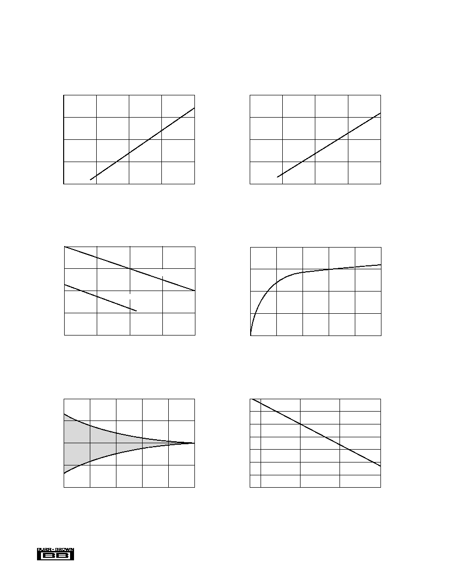
A common problem with many IC op amps and instrumentation amplifiers is shown in (a). Here, the amplifier's input is driven beyond its linear common-mode
range, forcing the output of the amplifier into the supply rails. The output then "folds back", i.e., a more positive input voltage now causes the output of the amplifier
to go negative. The INA103 has protection circuitry to prevent fold-back, and as shown in (b), limits cleanly.
(a) AD625 G = 1, V
IN
=
±
15V, R
L
= 600
(b) INA103 G = 1, V
IN
=
±
15V, R
L
= 600
FIGURE 9. INA103 Overload Condition Performance.
11
10
7
V
IN
16
15
13
14
6
2
1
INA103
V
OUT
R
G
V+
V≠
MJ15012
100
MJ15011
(To headphone
or speaker)
Buffer inside feedback loop
11
10
7
16
15
13
14
6
2
1
INA103
20
CMR
Trim
10
V
IN
Gain = 1V/V
(0dB)
Introduces
approximately
+0.2% Gain Error.
FIGURE 11. Increasing Output Circuit Drive.
FIGURE 10. Optional Circuit for Externally Trimming CMR.

Æ
INA103
12
FIGURE 12. Microphone Preamplifier with Provision for Phantom Power Microphones.
FIGURE 13. Instrumentation Amplifier with Shield Driver.
FIGURE 14. Gain-of-100 INA103 with FET Buffers.
11
10
7
V
IN
16
15
13
14
6
2
1
INA103
V
IN
V = 100
OUT
≠
+
OPA627
≠
+
OPA627
Gain = 100V/V
(40dB)
11 10
7
16
15
13
14
6
2
1
V
OUT
INA103
10
1k
Gain
Adjust
2.2k
240
47µF/63V
+
2.2k
240
47µF/63V
+
+48V
20dB
Pad
20dB
Pad
47k
6.8k
6.8k
1
3
2
cm
1µF
100k
≠
+
OPA627
Phantom
Power
Output offset voltage
control loop.
12
5
16
15
13
14
6
2
1
INA103
11
10
7
V
OUT
10k
10k
V
IN
≠
+
10k
10k
OPA602
100
Shield driver minimizes degradation of CMR due
to distributed capacitance on the input lines.