 | –≠–ª–µ–∫—Ç—Ä–æ–Ω–Ω—ã–π –∫–æ–º–ø–æ–Ω–µ–Ω—Ç: ISO102 | –°–∫–∞—á–∞—Ç—å:  PDF PDF  ZIP ZIP |

1
Æ
ISO102/106
International Airport Industrial Park ∑ Mailing Address: PO Box 11400 ∑ Tucson, AZ 85734 ∑ Street Address: 6730 S. Tucson Blvd. ∑ Tucson, AZ 85706
Tel: (520) 746-1111 ∑ Twx: 910-952-1111 ∑ Cable: BBRCORP ∑ Telex: 066-6491 ∑ FAX: (520) 889-1510 ∑ Immediate Product Info: (800) 548-6132
ISO102
ISO106
DESCRIPTION
The ISO102 and ISO106 isolation buffer amplifiers
are two members of our series of capacitive coupled
isolation products from Burr-Brown. They have the
same electrical performance and they differ in accu-
racy. The ISO102 is rated for 1500Vrms in a 24-pin
DIP. The ISO106 is rated for 3500Vrms in a 40-pin
DIP. Both side-brazed DIPs are 600mil wide and have
industry standard package dimensions with the excep-
tion of missing pins between input and output stages.
This permits utilization of automatic insertion tech-
niques in production. The three-chip hybrid with its
generous high voltage spacing is easy to use (no
external components are required).
Each buffer accurately isolates
±
10V analog signals
by digitally encoding the input voltage and uniquely
coupling across a differential ceramic capacitive bar-
FEATURES
q
14-BIT LINEARITY
q
INDUSTRY'S FIRST HERMETIC
ISOLATION AMPLIFIERS AT LOW COST
q
EASY-TO-USE COMPLETE CIRCUIT
q
RUGGED BARRIER, HV CERAMIC
CAPACITORS
q
100% TESTED FOR HIGH VOLTAGE
BREAKDOWN
ISO102: 4000Vrms/10s, 1500Vrms/1min
ISO106: 8000Vpk/10s, 3500Vrms/1min
q
ULTRA HIGH IMR: 125dB min at 60Hz,
ISO106
q
WIDE INPUT RANGE: ≠10V to +10V
q
WIDE BANDWIDTH: 70kHz
q
VOLTAGE REFERENCE OUTPUT: 5VDC
SIGNAL ISOLATION BUFFER AMPLIFIERS
Covered by patent number 4,748,419 and others pending.
+V
≠V
CC1
CC1
Gain
Adjust
+V
≠V
CC2
CC2
Digital
Common
Isolation
Barrier
V
IN
Offset
Adjust
Offset
Common
1
Reference
1
+5V
Common
2
Reference
2
C
2
C
1
V
OUT
+5V
rier. All elements necessary for operation are con-
tained within the DIP. This provides compact signal
isolation in a hermetic package.
APPLICATIONS
q
INDUSTRIAL PROCESS CONTROL
Transducer channel isolator for thermo-
couples, RTDs, pressure bridges, flow
meters
q
4mA TO 20mA LOOP ISOLATION
q
MOTOR AND SCR CONTROL
q
GROUND LOOP ELIMINATION
q
BIOMEDICAL/ANALYTICAL
MEASUREMENTS
q
POWER PLANT MONITORING
q
DATA ACQUISITION/TEST EQUIPMENT
ISOLATION
q
MILITARY EQUIPMENT
© 1987 Burr-Brown Corporation
PDS-716F
Printed in U.S.A. January, 1995
Æ

2
Æ
ISO102/106
SPECIFICATIONS
ELECTRICAL
At T
A
= +25
∞
C and V
CC1
= V
CC2
=
±
15V unless otherwise noted.
ISO102, ISO106, ISO102B, ISO106B
PARAMETER
CONDITIONS
MIN
TYP
MAX
UNITS
ISOLATION
Voltage
Rated Continuous
(1)
ISO102: AC, 60Hz
T
MIN
to T
MAX
1500
Vrms
DC
T
MIN
to T
MAX
2121
VDC
ISO106: AC, 60Hz
T
MIN
to T
MAX
3500
Vrms
DC
T
MIN
to T
MAX
4950
VDC
Test Breakdown, AC, 60Hz
ISO102
10s
4000
Vrms
ISO106
10s
8000
Vpk
Isolation-Mode Rejection
(2)
V
ISO
= Rated Continuous, 60Hz
AC: ISO102
115
120
dB
1
2
µ
Vrms/V
ISO106
125
130
dB
0.3
0.6
µ
Vrms/V
DC
140
160
dB
0.01
0.10
µ
VDC/V
Barrier Resistance
10
14
Barrier Capacitance
6
pF
Leakage Current
V
ISO
= 240Vrms, 60Hz
0.5
1
µ
Arms
INPUT
Voltage Range
Rated Operation
≠10
+10
V
Resistance
75
100
k
Capacitance
5
pF
OUTPUT
Voltage Range
Rated Operation
≠10
+10
V
Derated Operation
≠12
+12
V
Current Drive
±
5
mA
Short Circuit Current
9
20
50
mA
Ripple Voltage
(6)
f = 0.5MHz to 1.5MHz
3
mVp-p
Resistance
0.3
1
Capacitive Load Drive Capability
10,000
pF
Overload Recovery Time, 0.1%
|
V
O
|
> 12V
30
µ
s
OUTPUT VOLTAGE NOISE
Voltage: f = 0.1Hz to 10Hz
300
µ
Vp-p
f = 0.1Hz to 70kHz
16
µ
V/ Hz
Dynamic Range
(7)
: f = 0.1Hz to 70kHz
12-Bit Resolution, 1LSB, 20V FS
74
dB
f = 0.1Hz to 280Hz
16-Bit Resolution, 1LSB, 20V FS
96
dB
FREQUENCY RESPONSE
Small Signal Bandwidth
70
kHz
Full Power Bandwidth, 0.1% THD
V
O
=
±
10V
5
kHz
Slew Rate
V
O
=
±
10V
0.5
V/
µ
s
Settling Time, 0.1%
V
O
= ≠10V to +10V
100
µ
s
Overshoot, Small Signal
(8)
C
1
= C
2
= 0
40
%
VOLTAGE REFERENCES
Voltage Output, Ref
1
, Ref
2
No Load
+4.975
+5
+5.025
VDC
B Grade
No Load
+4.995
+5
+5.005
VDC
vs Temperature
±
5
20
ppm/
∞
C
vs Supplies
10
µ
V/V
vs Load
400
1000
µ
V/mA
Current Output
≠0.1
+5
mA
Short Circuit Current
6
14
30
mA
POWER SUPPLIES
Rated Voltage,
±
V
CC1
,
±
V
CC2
Rated Performance
±
15
V
Voltage Range
±
10
±
20
V
Quiescent Current: +V
CC1
No Load
+11
+15
mA
≠V
CC1
≠9
≠12
mA
+V
CC2
+25
+33
mA
≠V
CC2
≠15
≠20
mA
Dissipation:
±
V
CC1
300
400
mW
±
V
CC2
600
800
mW
TEMPERATURE RANGE
Specification
≠25
+85
∞
C
Operating
(9)
≠25
+85
∞
C
Storage
≠65
+150
∞
C
Thermal Resistance,
JA
40
∞
C/W
JC
12
∞
C/W
3
Æ
ISO102/106
ORDERING INFORMATION
TEMPERATURE
MODEL
PACKAGE
RANGE
ISO102
Ceramic
≠25
∞
C to +85
∞
C
ISO102B
Ceramic
≠25
∞
C to +85
∞
C
ISO106
Ceramic
≠25
∞
C to +85
∞
C
ISO106B
Ceramic
≠25
∞
C to +85
∞
C
ELECTRICAL (CONT)
ISO102
ISO102B
PARAMETER
CONDITIONS
MIN
TYP
MAX
MIN
TYP
MAX
UNITS
GAIN
Nominal Gain
1
*
V/V
Initial Error
(3)
±
0.1
±
0.25
0.07
0.13
% FSR
Gain vs Temperature
±
20
±
50
±
12
±
25
ppm FSR/
∞
C
Nonlinearity
(4)
V
O
= ≠10V to +10V
±
0.007
±
0.012
±
0.002
±
0.003
% FSR
INPUT OFFSET VOLTAGE
Initial Offset
V
IN
= 0V
±
25
±
70
±
15
±
25
mV
vs Temperature
±
250
±
500
±
150
±
250
µ
V/
∞
C
vs Power Supplies
(5)
Input Stage, V
CC1
=
±
10V to
±
20V
0
1.4
4.0
*
*
*
mV/V
Output Stage, V
CC2
=
±
10V to
±
20V
≠4
≠1.4
0
*
*
*
mV/V
The information provided herein is believed to be reliable; however, BURR-BROWN assumes no responsibility for inaccuracies or omissions. BURR-BROWN assumes
no responsibility for the use of this information, and all use of such information shall be entirely at the user's own risk. Prices and specifications are subject to change
without notice. No patent rights or licenses to any of the circuits described herein are implied or granted to any third party. BURR-BROWN does not authorize or warrant
any BURR-BROWN product for use in life support devices and/or systems.
ISO106
ISO106B
PARAMETER
CONDITIONS
MIN
TYP
MAX
MIN
TYP
MAX
UNITS
GAIN
Nominal Gain
1
*
V/V
Initial Error
(3)
±
0.1
±
0.25
0.07
*
% FSR
Gain vs Temperature
±
20
±
50
±
12
±
25
ppm FSR/
∞
C
Nonlinearity
(4)
V
O
= ≠10V to +10V
±
0.04
±
0.075
±
0.007
±
0.025
% FSR
INPUT OFFSET VOLTAGE
Initial Offset
V
IN
= 0V
±
25
±
70
*
*
mV
vs Temperature
±
250
±
500
±
150
±
250
µ
V/
∞
C
vs Power Supplies
(5)
Input Stage, V
CC1
=
±
10V to
±
20V
3.7
*
mV/V
Output Stage, V
CC2
=
±
10V to
±
20V
≠3.7
*
mV/V
* Specification same as model to the left.
NOTES: (1) 100% tested at rated continuous for one minute. (2) Isolation-mode rejection is the ratio of the change in output voltage to a change in isolation barrier voltage.
It is a function of frequency as shown in the Typical Performance Curves. This is specified for barrier voltage slew rates not exceeding 100V/
µ
s. (3) Adjustable to zero.
FSR = Full Scale Range = 20V. (4) Nonlinearity is the peak deviation of the output voltage from the best fit straight line. It is expressed as the ratio of deviation to FSR.
(5) Power supply rejection = change in V
OS
/20V supply change. (6) Ripple is the residual component of the barrier carrier frequency generated internally. (7) Dynamic
range = FSR/(voltage spectral noise density
x
square root of user bandwidth). (8) Overshoot can be eliminated by band-limiting. (9) See "Power Dissipation vs
Temperature" performance curve for limitations. (10) Band limited to 10Hz, bypass capacitors located less than 0.25" from supply pins.
PACKAGE INFORMATION
(1)
PACKAGE DRAWING
MODEL
PACKAGE
NUMBER
ISO102
24-Pin Ceramic
208
ISO102B
24-Pin Ceramic
208
ISO106
40-Pin Ceramic
206
ISO106B
40-Pin Ceramic
206
NOTE: (1) For detailed drawing and dimension table, please see end of data
sheet, or Appendix D of Burr-Brown IC Data Book.
ABSOLUTE MAXIMUM RATINGS
Supply Without Damage ....................................................................
±
20V
Input Voltage Range ..........................................................................
±
50V
Transient Immunity, dV/dt .......................................................... 100kV/
µ
s
Continuous Isolation Voltage Across Barrier
ISO102 .................................................................................... 1500Vrms
ISO106 .................................................................................... 3500Vrms
Junction Temperature .................................................................... +160
∞
C
Storage Temperature Range ......................................... ≠65
∞
C to +150
∞
C
Lead Temperature (soldering, 10s) ............................................... +300
∞
C
Amplifier and Reference Output
Short Circuit Duration ....................................... Continuous to Common
4
Æ
ISO102/106
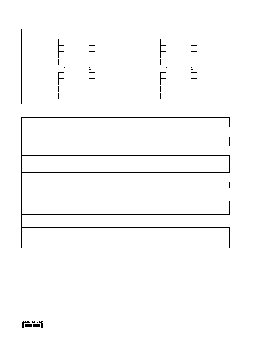
PIN CONFIGURATION
≠V
V
Gain Adjust
Common
C
Common
Reference
+V
+V
Offset Adjust
Offset
Reference
Digital Common
C
V
≠V
1
2
3
4
9
10
11
12
24
23
22
21
16
15
14
13
CC1
CC2
CC1
ISO102
1
OUT
CC2
2
Isolation
Barrier
IN
1
1
2
2
≠V
V
Gain Adjust
Common
C
Common
Reference
+V
+V
Offset Adjust
Offset
Reference
Digital Common
C
V
≠V
1
2
3
4
17
18
19
20
40
39
38
37
24
23
22
21
CC1
CC2
CC1
ISO106
1
OUT
CC2
2
Isolation
Barrier
IN
1
1
2
2
PIN DESCRIPTIONS
±
V
CC1
,
Positive and negative power supply voltages and common (or ground) for the input stage. Common
1
is the analog reference voltage for input
Common
1
signals. The voltage between Common
1
and Common
2
is the isolation voltage and appears across the internal high voltage barrier.
±
V
CC2
,
Positive and negative power supply voltages and common (or ground) for the output stage. Common
2
is the analog reference voltage for output
Common
2
signals. The voltage between Common
1
and Common
2
is the isolation voltage and appears across the internal high voltage barrier.
V
IN
Signal input pin. Input impedance is typically 100k
. The input range is rated for
±
10V. The input level can actually exceed the input stage
supplies. Output signal swing is limited only by the output supply voltages.
Gain
This pin is an optional signal input. A series 5k
potentiometer between this pin and the input signal allows a guaranteed
±
1.5% gain adjustment
Adjust
range. When gain adjustment is not required, the Gain Adjust should be left open. Figure 4 illustrates the gain adjustment connection.
Reference
1
+5V reference output. This low-drift zener voltage reference is necessary for setting the bipolar offset point of the input stage. This pin must
be strapped to either Offset or Offset Adjust to allow the isolation amplifier to function. The reference is often useful for input signal
conditioning circuits. See "Effect of Reference Loading on Offset" performance curve for the effect of offset voltage change with reference loading.
Reference
1
is identical to, but independent of, Reference
2
. This output is short circuit protected.
Reference
2
+5V reference output. This reference circuit is identical to, but independent of, Reference
1
. It controls the bipolar offset of the output stage through
an internal connection. This output is short-circuit protected.
Offset
Offset input. This input must be strapped to Reference
1
unless user adjustment of bipolar offset is required.
Offset
This pin is for optional offset control. When connected to the Reference
1
pin through a 1k
potentiometer,
±
150mV of adjustment range is
Adjust
guaranteed. Under this condition, the Offset pin should be connected to the Offset Adjust pin. When offset adjustment is not required, the Offset
Adjust pin is left open. See Figure 4.
Digital
Digital common or ground. This separate ground carries currents from the digital portions of the output stage circuit. The best grounding practi-
Common
ces require that digital common current does not flow in analog common connections. Both pins can be tied directly to a ground plane if available.
Difference in potentials between the Common
2
and Digital Common pins can be
±
1V. See Figure 2.
V
OUT
Signal output. Because the isolation amplifier has unity gain, the output signal is ideally identical to the input signal. The output is low impedance
and is short-circuit protected. This signal is referenced to Common
2
; subsequent circuitry should have a separate "sense" connection to Common
1
as well as V
OUT
.
C
1
, C
2
Capacitors for small signal bandwidth control. These pins connect to the internal rolloff frequency controlling nodes of the output low-pass filter.
Additional capacitance added to these pins will modify the bandwidth of the buffer. C
2
is always twice the value of C
1
. See "Bandwidth Control"
performance curve for the relationship between bandwidth and C
1
and C
2
. When no connections are made to these pins, the full small-signal
bandwidth is maintained. Be sure to shield C
1
and C
2
pins from high electric fields on the PC board. This preserves AC isolation-mode rejection
by reducing capacitive coupling effects.

5
Æ
ISO102/106
TYPICAL PERFORMANCE CURVES
T
A
= +25
∞
C, V
CC
=
±
15VDC unless otherwise noted.
ISOLATION-MODE REJECTION
vs ISOLATION VOLTAGE FREQUENCY
Isolation Voltage Frequency (Hz)
Isolation-Mode Rejection (dB)
160
140
120
100
80
60
10
1M
100
1k
10k
100k
ISO102
ISO106
DYNAMIC RANGE vs BANDWIDTH
Small Signal Bandwidth (Hz)
Bandwidth Control Capacitors (F)
Dynamic Range (dB)
120
110
100
90
80
70
1
10
100
1k
10k
100k
3µ
300n
30n
3nF
300p
30p
BW --
C --
1
See "Bandwidth
Control" Curve
See Figure 4
V
OUT
= ±1V
V
OUT
= ±10V
ISOLATION LEAKAGE CURRENT
vs ISOLATION VOLTAGE FREQUENCY
Isolation Voltage Frequency (Hz)
Isolation Leakage Current (A)
10
1M
10m
1m
100µ
10µ
1µ
100n
100
1k
10k
100k
Isolation Voltage = 240Vrms
Isolation Voltage (V)
0
Rated
1
0.5
0
≠0.5
≠1
2
1
0
≠1
≠2
Gain
Offset
T = T
to T
MIN
MAX
GAIN ERROR AND
OFFSET VOLTAGE
vs ISOLATION VOLTAGE
Gain Error (%)
Offset Voltage (mV)
BANDWIDTH CONTROL
C
1
(F)
Small Signal Bandwidth (Hz)
1M
100k
10k
1k
100
10
1
3p
30p
300p
3n
30n
300n
3µ
C
2
= 2 (C
1
)
See Figure 4
POWER DISSIPATION vs TEMPERATURE
Ambient Temperature (∞C)
Maximum Power Dissipation (W)
≠25
85
95
105
115
125
135
1.6
1.4
1.2
1
0.8
0
Maximum Power Supplies (V)
±20
±15
±10
0.785
1.178
1.57
= (T
≠ T )/
A
Slope =
P
= 40∞C/W
JA
D MAX
J MAX
JA
Maximum Junction
Temperature = 160∞C
Maximum Junction
Temperature = 150∞C
0