 | –≠–ª–µ–∫—Ç—Ä–æ–Ω–Ω—ã–π –∫–æ–º–ø–æ–Ω–µ–Ω—Ç: ISO103 | –°–∫–∞—á–∞—Ç—å:  PDF PDF  ZIP ZIP |
Low-Cost, Internally Powered
ISOLATION AMPLIFIER
FEATURES
q
SIGNAL AND POWER IN ONE
DOUBLE-WIDE (0.6") SIDE-BRAZED
PACKAGE
q
5600Vpk TEST VOLTAGE
q
1500Vrms CONTINUOUS AC BARRIER
RATING
q
WIDE INPUT SIGNAL RANGE:
≠10V to +10V
q
WIDE BANDWIDTH:
20kHz Small Signal, 20kHz Full Power
q
BUILT-IN ISOLATED POWER:
±
10V to
±
18V Input,
±
50mA Output
q
MULTICHANNEL SYNCHRONIZATION
CAPABILITY (TTL)
q
BOARD AREA ONLY 0.72in.
2
(4.6cm
2
)
APPLICATIONS
q
MULTICHANNEL ISOLATED DATA
ACQUISITION
q
ISOLATED 4-20mA LOOP RECEIVER AND
POWER
q
POWER SUPPLY AND MOTOR CONTROL
q
GROUND LOOP ELIMINATION
ISO103
DESCRIPTION
The ISO103 isolation amplifier provides both signal
and power across an isolation barrier. The ceramic
non-hermetic hybrid package with side-brazed pins
contains a transformer-coupled DC/DC converter and
a capacitor-coupled signal channel.
Extra power is available on the isolated input side for
external input conditioning circuitry. The converter is
protected from shorts to ground with an internal cur-
rent limit, and the soft-start feature limits the initial
currents from the power source. Multiple-channel syn-
chronization can be accomplished by applying a TTL
clock signal to paralleled Sync pins. The Enable con-
trol is used to turn off transformer drive while keeping
the signal channel demodulator active. This feature
provides a convenient way to reduce quiescent current
for low power applications.
The wide barrier pin spacing and internal insulation
allow for the generous 1500Vrms continuous rating.
Reliability is assured by 100% barrier breakdown
testing that conforms to UL1244 test methods. Low
barrier capacitance minimizes AC leakage currents.
These specifications and built-in features make the
ISO103 easy to use, as well as providing for compact
PC board layouts.
Duty Cycle
Modulator
Duty Cycle
Demodulator
Rectifiers
Filters
Oscillator
Driver
Sense
V
OUT
Com 2
≠V
CC2
Sync*
Enable
+V
CC2
Gnd 2
+V
CC1
≠V
CC1
Gnd 1
Com 1
V
IN
Ps Gnd
≠V
C
+V
C
Sync
*Ground if not used
Æ
International Airport Industrial Park ∑ Mailing Address: PO Box 11400, Tucson, AZ 85734 ∑ Street Address: 6730 S. Tucson Blvd., Tucson, AZ 85706 ∑ Tel: (520) 746-1111
Twx: 910-952-1111 ∑ Internet: http://www.burr-brown.com/ ∑ Cable: BBRCORP ∑ Telex: 066-6491 ∑ FAX: (520) 889-1510 ∑ Immediate Product Info: (800) 548-6132
ISO103
©
1989 Burr-Brown Corporation
PDS-1004E
Printed in U.S.A. August, 1999
Æ
ISO103
2
SPECIFICATIONS
ELECTRICAL
At T
A
= +25
∞
C and V
CC2
=
±
15V,
±
15mA output current unless otherwise noted.
ISO103
ISO103B
PARAMETER
CONDITIONS
MIN
TYP
MAX
MIN
TYP
MAX
UNITS
ISOLATION
Rated Continuous Voltage
(1)
AC, 60Hz
T
MIN
to T
MAX
1500
T
Vrms
DC
T
MIN
to T
MAX
2121
T
VDC
Test Breakdown, 100% AC, 60Hz
10s
5657
T
Vpk
Isolation-Mode Rejection
1500Vrms, 60Hz
130
T
dB
2121VDC
160
T
dB
Barrier Impedance
10
12
|| 9
T
|| pF
Leakage Current
240Vrms, 60Hz
1
2
T
T
µ
A
GAIN
Nominal
1
T
V/V
Initial Error
±
0.12
±
0.3
±
0.08
±
0.15
% FSR
Gain vs Temperature
±
60
±
100
±
20
±
50
ppm/
∞
C
Nonlinearity
V
O
= ≠10V to 10V
±
0.026
±
0.075
±
0.018
±
0.050
% FSR
V
O
= ≠5V to 5V
±
0.009
T
±
0.025
%FSR
INPUT OFFSET VOLTAGE
Initial Offset
±
20
±
60
T
T
mV
vs Temperature
±
300
±
500
T
T
µ
V/
∞
C
vs Power Supplies
V
CC2
=
±
10V to
±
18V
0.9
T
mV/V
vs Output Supply Load
I
O
= 0 to
±
50mA
±
0.3
T
mV/mA
SIGNAL INPUT
Voltage Range
Output Voltage in Range
±
10
±
15
T
T
V
Resistance
200
T
k
SIGNAL OUTPUT
Voltage Range
±
10
±
12.5
T
T
V
Current Drive
±
5
±
15
T
T
mA
Ripple Voltage, 800kHz Carrier
25
T
mVp-p
400
/4.7nF (See Figure 4)
5
T
mVp-p
Capacitive Load Drive
1000
T
pF
Voltage Noise
4
T
µ
V/
Hz
FREQUENCY RESPONSE
Small Signal Bandwidth
20
T
kHz
Slew Rate
1.5
T
V/
µ
s
Settling Time
0.1%, ≠10/10V
75
T
µ
s
POWER SUPPLIES
Rated Voltage, V
CC2
±
15
T
V
Voltage Range
±
10
±
18
T
T
V
Input Current
I
O
=
±
15mA
+90/≠4.5
T
mA
I
O
= 0mA
+60/≠4.5
T
mA
Ripple Current
No Filter
60
T
mAp-p
C
IN
= 1
µ
F
3
T
mAp-p
Rated Output Voltage
Load = 15mA
±
14.25
±
15
±
15.75
T
T
T
V
Output
50mA Balanced Load
10
T
T
V
100mA Single-Ended Loads
10
T
T
V
Load Regulation
Balanced Load
0.3
T
%/mA
Line Regulation
1.12
T
V/V
Output Voltage vs Temperature
2.5
T
mV/
∞
C
Voltage Balance Error,
±
V
CC1
0.05
T
%
Voltage Ripple (800kHz)
No External Capacitors
50
T
mVp-p
C
EXT
= 1
µ
F
5
T
mVp-p
Output Capacitive Load
1
T
µ
F
Sync Frequency
Sync-Pin Grounded
(2)
1.6
T
MHz
TEMPERATURE RANGE
Specification
≠25
+85
T
T
∞
C
Operating
≠25
+85
T
T
∞
C
Storage
≠25
+125
T
T
∞
C
T
Specifications same as ISO103.
NOTE: (1) Conforms to UL1244 test methods. 100% tested at 1500Vrms for 1 minute. (2) If using external synchronization with a TTL-level clock, frequency should
be between 1.2MHz and 2MHz with a duty-cycle greater than 25%.
3
Æ
ISO103
ABSOLUTE MAXIMUM RATINGS
Supply Without Damage ....................................................................
±
18V
V
IN
, Sense Voltage .............................................................................
±
50V
Com 1 to Gnd 1 or Com 2 to Gnd 2 ..............................................
±
200mV
Enable, Sync ........................................................................... 0V to +V
CC2
Continuous Isolation Voltage ..................................................... 1500Vrms
V
ISO
, dv/dt ..................................................................................... 20kV/
µ
s
Junction Temperature ...................................................................... 150
∞
C
Storage Temperature ...................................................... ≠25
∞
C to +125
∞
C
Lead Temperature,10s .................................................................... 300
∞
C
Output Short to Gnd 2 Duration ............................................... Continuous
±
V
CC1
to Gnd 1 Duration .......................................................... Continuous
1
2
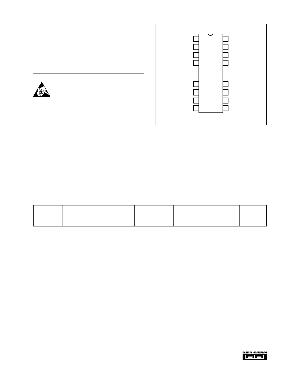
+V
CC1
3
4
9
Com 2
10
V
OUT
11
Sense
12
Gnd 2
24
23 Gnd 1
22 V
IN
21 Com 1
≠V
CC2
16
Sync*
15
+V
CC2
Enable
PIN CONFIGURATION
*Operation requires this pin be grounded or driven with TTL levels.
+V
C
≠V
CC1
Ps Gnd
13
14
≠V
CC1
Any integrated circuit can be damaged by ESD. Burr-Brown
recommends that all integrated circuits be handled with
appropriate precautions. Failure to observe proper handling
and installation procedures can cause damage.
ESD damage can range from subtle performance degrada-
tion to complete device failure. Precision integrated circuits
may be more susceptible to damage because very small
parametric changes could cause the device not to meet
published specifications.
The information provided herein is believed to be reliable; however, BURR-BROWN assumes no responsibility for inaccuracies or omissions. BURR-BROWN assumes
no responsibility for the use of this information, and all use of such information shall be entirely at the user's own risk. Prices and specifications are subject to change
without notice. No patent rights or licenses to any of the circuits described herein are implied or granted to any third party. BURR-BROWN does not authorize or warrant
any BURR-BROWN product for use in life support devices and/or systems.
ELECTROSTATIC
DISCHARGE SENSITIVITY
PACKAGE
SPECIFIED
DRAWING
TEMPERATURE
PACKAGE
ORDERING
TRANSPORT
PRODUCT
PACKAGE
NUMBER
(1)
RANGE
MARKING
NUMBER
(2)
MEDIA
ISO103
24-Pin DIP
231
≠25
∞
C to +85
∞
C
NOTES: (1) For detailed drawing and dimension table, please see end of data sheet, or Appendix C of Burr-Brown IC Data Book. (2) Models with a slash (/) are
available only in Tape and Reel in the quantities indicated (e.g., /2K5 indicates 2500 devices per reel). Ordering 2500 pieces of "ISO103/2K5" will get a single 2500-
piece Tape and Reel. For detailed Tape and Reel mechanical information, refer to Appendix B of Burr-Brown IC Data Book.
PACKAGE/ORDERING INFORMATION
Æ
ISO103
4
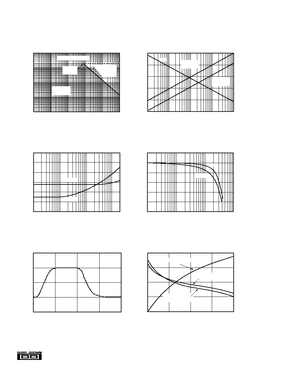
TYPICAL PERFORMANCE CURVES
At T
A
= +25
∞
C, V
CC2
=
±
15VDC,
±
15mA output current, unless otherwise noted.
RECOMMENDED RANGE OF ISOLATION VOLTAGE
100
1k
10k
100k
1M
10M
10k
2.1k
1k
100
10
1
Maximum Isolation Voltage (Vpk)
Barrier Voltage Rating
Non-Specified
Signal
Operation
2100V
at 75kHz
Operational
Region
Isolation Voltage Frequency (Hz)
IMR/LEAKAGE vs FREQUENCY
140
130
120
110
100
10
100
1k
10k
100k
10m
1m
100µ
10µ
1µ
100n
Leakage at
1500Vrms
Leakage at
240Vrms
IMR
Isolation Voltage Frequency (Hz)
Isolation-Mode Rejection (dB)
Barrier Leakage Current (Arms)
90
DISTORTION vs FREQUENCY
20
100
1k
10k
Frequency (Hz)
THD+N (%)
20k
10
3
1
0.3
0.1
0.03
0.01
V = 2Vp-p
O
V = 20Vp-p
O
GAIN/PHASE vs FREQUENCY
1k
100
10k
100k
Small Signal Frequency (Hz)
3
0
≠3
≠9
≠12
≠15
≠6
Gain (dB)
0
45
90
135
180
Phase Shift (∞)
GAIN
PHASE
20
10
0
≠10
≠20
Output Voltage (V)
Time (µs)
0
50
100
LARGE SIGNAL TRANSIENT RESPONSE
ISOLATED POWER SUPPLY
LOAD REGULATION AND EFFICIENCY
±V Supply Output Current (mA)
CC1
10
20
20
40
30
60
40
80
0
15
30
45
60
17
16
15
14
13
±V Output Voltage (V)
CC1
Output Voltage
Single-Ended Loads
Efficiency (%)
0
0
Output Voltage
Balanced Loads
Balanced Load Efficiency
5
Æ
ISO103
TYPICAL PERFORMANCE CURVES
(CONT)
At T
A
= +25
∞
C, V
CC2
=
±
15VDC,
±
15mA output current, unless otherwise noted.
ISOLATED POWER SUPPLY LINE REGULATION
9
10
11
12
13
14
15
16
17
18
19
+V (V)
CC2
19
18
17
16
15
14
13
12
11
10
9
+V (V)
CC1
±15mA Load
1.12V/V
ISOLATION POWER SUPPLY VOLTAGE
vs TEMPERATURE
≠25
0
25
50
75
100
Temperature (∞C)
2
1
0
≠1
≠2
V (%)
CC2
ISOLATED SUPPLY VOLTAGE AND V
vs SYNC FREQUENCY
OS
1
1.5
2
2.5
5
2.5
≠2.5
≠5
0
250
125
0
≠125
≠250
V (mV)
OS
V (mV)
CC1
Sync Frequency (MHz)
V
CC1
V
OS