 | –≠–ª–µ–∫—Ç—Ä–æ–Ω–Ω—ã–π –∫–æ–º–ø–æ–Ω–µ–Ω—Ç: ISO130 | –°–∫–∞—á–∞—Ç—å:  PDF PDF  ZIP ZIP |

49%
FPO
ISO130
FEATURES
q
HIGH ISOLATION-MODE REJECTION:
10kV/
µ
s (min)
q
LARGE SIGNAL BANDWIDTH: 85kHz (typ)
q
DIFFERENTIAL INPUT/DIFFERENTIAL
OUTPUT
q
VOLTAGE OFFSET DRIFT vs
TEMPERATURE: 4.6
µ
V/
∞
C (typ)
q
OFFSET VOLTAGE 1.8mV (max)
q
INPUT REFERRED NOISE: 300
µ
Vrms (typ)
q
NONLINEARITY: 0.25% (max)
q
SINGLE SUPPLY OPERATION
q
SIGMA-DELTA A/D CONVERTER
TECHNOLOGY
q
WORLDWIDE SAFETY APPROVAL:
UL1577 (File No. E162573), VDE0884
(File No. 85511), CSA22.2 (File No. 88324)
q
AVAILABLE IN 8-PIN PLASTIC DIP and
8-PIN GULL-WING PLASTIC SURFACE
MOUNT
APPLICATIONS
q
MOTOR AND SCR CONTROL
q
MOTOR PHASE CURRENT SENSING
q
INDUSTRIAL PROCESS CONTROL:
Transducer Isolator, Isolator for
Thermocouples, RTDs
q
GENERAL PURPOSE ANALOG SIGNAL
ISOLATION
q
POWER MONITORING
q
GROUND LOOP ELIMINATION
DESCRIPTION
The ISO130 is a high isolation-mode rejection, isola-
tion amplifier suited for motor control applications. Its
versatile design provides the precision and stability
needed to accurately monitor motor currents in high-
noise motor control environments. The ISO130 can
also be used for general analog signal isolation appli-
cations requiring stability and linearity under severe
noise conditions.
The signal is transmitted digitally across the isolation
barrier optically, using a high-speed AlGaAs LED.
The remainder of the ISO130 is fabricated on 1
µ
m
CMOS IC process. A sigma-delta analog-to-digital
converter, chopper stabilized amplifiers and differen-
tial input and output topologies make the isolation
amplifier suitable for a variety of applications.
The ISO130 is easy to use. No external components
are required for operation. The key specifications are
10kV/
µ
s isolation-mode rejection, 85kHz large signal
bandwidth, and 4.6
µ
V/
∞
C V
OS
drift. A single power
supply ranging from +4.5V to +5.5V makes this am-
plifier ideal for low power isolation applications.
The ISO130 is available in 8-pin plastic DIP and 8-pin
plastic gull-wing surface mount packages.
Æ
High IMR, Low Cost
ISOLATION AMPLIFIER
© 1994 Burr-Brown Corporation
PDS-1234B
Printed in U.S.A. June, 1995
1
2
3
4
8
7
6
5
V
S1
V
IN+
V
IN≠
GND
1
V
S2
V
OUT+
V
OUT≠
GND
2
IMR SHIELD
International Airport Industrial Park ∑ Mailing Address: PO Box 11400 ∑ Tucson, AZ 85734 ∑ Street Address: 6730 S. Tucson Blvd. ∑ Tucson, AZ 85706
Tel: (520) 746-1111 ∑ Twx: 910-952-1111 ∑ Cable: BBRCORP ∑ Telex: 066-6491 ∑ FAX: (520) 889-1510 ∑ Immediate Product Info: (800) 548-6132

Æ
ISO130
2
ISO130P, ISO130PB
ISO130U, ISO130UP
PARAMETER
CONDITIONS
MIN
TYP
MAX
UNITS
ISOLATION
Input-Output Surge Withstand Voltage
(8, 9)
,
t = 1
MIN
, RH
50%
(In accordance with UL1577)
3750
Vrms
Barrier Impedance
(9)
Resistance
V
ISO
= 500VDC
10
13
Capacitance
f = 1MHz
0.7
pF
Isolation Mode Voltage Errors
Rising Edge Transient Immunity
V
IM
= 1kV,
V
OUT
< 50mV
10
25
kV/
µ
s
Falling Edge Transient Immunity
V
IM
= 1kV,
V
OUT
< 50mV
10
15
kV/
µ
s
Isolation Mode Rejection Ratio
(2)
> 140
dB
SPECIFICATIONS
ISOLATION SPECIFICATIONS ≠ VDE0884 INSULATION CHARACTERISTICS
At V
IN
≠, V
IN
≠ = 0V, T
A
= 25
∞
C, V
S1
, V
S2
= 5.0V unless otherwise noted.
SPECIFICATIONS
ISOLATION SPECIFICATIONS
At V
IN
+, V
IN
≠ = 0V, T
A
= 25
∞
C, V
S1
, V
S2
= 5.0V, unless otherwise noted.
ISO130P/ISO130PB
ISO130U/ISO130UB
PARAMETER
CONDITIONS
CHARACTERISTIC
UNITS
ISOLATION CHARACTERISTICS
Installation Classification
As Per VDE0109/12.83
Table I
Rated Mains Voltage
300Vrms
I-IV
Rated Mains Voltage
600Vrms
I-III
Climatic Classification
40/85/21
Pollution Degree
(1)
As Per VDE0109/12.83
2
Maximum Working Insulation Voltage (V
IORM
)
600
Vrms
Side A to Side B Test Voltage, Method b (V
PR
)
(9)
Partial Discharge < 5pC
V
PR
= 1.6 x V
IORM
, t
P
= 1s
960
Vrms
Side A to Side B Test Voltage, Method a (V
PR
)
(9)
Type and Sample Test
Partial Discharge < 5pC
V
PR
= 1.2 x V
IORM
, t
P
= 60s
720
Vrms
Highest Allowable Overvoltage (V
TR
)
(9)
Transient Overvoltage, t
TR
= 10s
6000
V
PEAK
Safety-Limiting Values
Case Temperature (T
SI
)
175
∞
C
Input Power (P
SI (INPUT)
)
80
mW
Output Power (P
SI (OUTPUT)
)
250
mW
INSULATION RELATED SPECIFICATIONS
Min. External Air Gap (clearance)
> 7
mm
Min. External Tracking Path (creepage)
8
mm
Internal Isolation Gap (clearance)
0.5
mm
Tracking Resistance (CTI)
175
V
Isolation Group
per VDE0109
III a
Insulation Resistance
25
∞
C, V
ISO
= 500V
10
11

3
Æ
ISO130
SPECIFICATIONS
At V
IN
+, V
IN
≠ = 0V, T
A
= 25
∞
C, V
S1
, V
S2
= 5.0V unless otherwise noted.
ISO130P/ISO130PB
ISO130U/ISO130UB
PARAMETER
CONDITIONS
MIN
TYP
MAX
UNITS
INPUT
Initial Offset Voltage
≠1.8
≠0.9
0.0
mV
vs Temperature
4.6
µ
V/
∞
C
vs V
S1
30
µ
V/V
vs V
S2
≠40
µ
V/V
Power Supply Rejection; V
S1
and V
S2
Together
1MHz Square Wave, 5ns Rise/Fall Time
5
mV/V
Noise
0.1Hz to 100kHz
300
µ
Vrms
Input Voltage Range
≠200
200
mV
Maximum Input Voltage Range before Output Clipping
±
300
mV
Initial Input Bias Current
(3)
≠670
nA
vs Temperature
3
nA/
∞
C
Input Resistance
(3)
530
k
vs Temperature
0.38
%/
∞
C
Common-Mode Rejection Ratio
(4)
72
dB
GAIN
(5)
Initial Gain
ISO130P/ISO130U
≠200mV < V
IN
+ < 200mV
7.61
8.00
8.40
V/V
ISO130PB/ISO130UB
≠200mV < V
IN
+ < 200mV
7.85
7.93
8.01
V/V
Gain vs Temperature
10
ppm/
∞
C
Gain vs V
S1
2.1
ppm/mV
Gain vs V
S2
≠0.6
ppm/mV
Gain Nonlinearity
for ≠200mV < V
IN
+ < 200mV
0.2
0.35
%
for ≠100mV < V
IN
+ < 100mV
0.1
0.25
%
vs Temperature
(6)
≠200mV < V
IN
+ < 200mV
≠0.001
% pts/
∞
C
vs V
S1
(6)
≠200mV < V
IN
+ < 200mV
≠0.005
% pts/V
vs V
S2
(6)
≠200mV < V
IN
+ < 200mV
≠0.007
% pts/V
OUTPUT
Voltage Range
High
V
IN
+ = +500mV
3.61
V
Low
V
IN
+ = ≠500mV
1.18
V
Common-Mode Voltage
≠40
∞
C < T
A
< 85
∞
C, 4.5V < V
S1
< 5.5V
2.2
2.39
2.6
V
Current Drive
(7)
1
mA
Short-Circuit Current
V
OUT
= 0V or V
OUT
= V
S2
9.3
mA
Output Resistance
11
vs Temperature
0.6
%/
∞
C
FREQUENCY RESPONSE
Bandwidth
≠3dB
≠40
∞
C to 85
∞
C
50
85
kHz
≠45
∞
35
kHz
Rise/Fall Time (10% - 90%)
≠40
∞
C to 85
∞
C
4.3
6.6
µ
s
Propagation Delay
to 10%
≠40
∞
C to 85
∞
C
2.0
3.3
µ
s
to 50%
≠40
∞
C to 85
∞
C
3.4
5.6
µ
s
to 90%
≠40
∞
C to 85
∞
C
6.3
9.9
µ
s
POWER SUPPLIES
Rated Voltage
5.0
V
Voltage Range
4.5
5.5
V
Quiescent Current
V
S1
V
IN
+ = 200mV, ≠40
∞
C < T
A
< 85
∞
C, 4.5V < V
S1
< 5.5V
10.7
15.5
mA
V
S2
≠40
∞
C < T
A
< 85
∞
C, 4.5V < V
S1
< 5.5V
11.6
15.5
mA
TEMPERATURE RANGE
Specification
≠40
85
∞
C
Operating
≠40
100
∞
C
Storage
≠55
125
∞
C
C≠A
86
∞
C/W
NOTES: (1) This part may also be used in Pollution Degree 3 environments where the rated mains voltage is 300Vrms (per DIN VDE0109/12.83). (2) IMRR
= 20 log (
V
IN
/
V
ISO
). (3) Time averaged value. (4) V
IN
+ = V
IN
≠ = V
CM
. CMRR = 20 log (
V
CM
/
V
OS
). (5) The slope of the best-fit line of (V
OUT+
≠ V
OUT≠
) vs
(V
IN+
≠V
IN≠
). (6) Change in nonlinearity vs temperature or supply voltage expressed in number of percentage points per
∞
C or volt. (7) For best offset voltage
performance. (8) For devices with minimum V
ISO
specified at 3750Vrms, each isolation amplifier is proof-tested by applying an insulation test voltage
4500Vrms for 1 second (leakage current < 5
µ
A). This specification does not guarantee continuous operation. (9) Pins 1-4 are shorted together and pins 5-
8 are shorted together for this test.

Æ
ISO130
4
PIN CONFIGURATION
The information provided herein is believed to be reliable; however, BURR-BROWN assumes no responsibility for inaccuracies or omissions. BURR-BROWN assumes
no responsibility for the use of this information, and all use of such information shall be entirely at the user's own risk. Prices and specifications are subject to change
without notice. No patent rights or licenses to any of the circuits described herein are implied or granted to any third party. BURR-BROWN does not authorize or warrant
any BURR-BROWN product for use in life support devices and/or systems.
ABSOLUTE MAXIMUM RATINGS
Supply Voltages: V
S1
, V
S2
......................................................... 0V to 5.5V
Steady-State Input Voltage .......................................... ≠2V to V
S1
+ 0.5V
2 Second Transient Input Voltage ................................................... ≠6.0V
Output Voltages: V
OUT
+, V
OUT
≠ ................................... ≠0.5V to V
S2
+ 0.5V
Lead Temperature Solder (1.6mm below seating plane, 10s) ....... 260
∞
C
PACKAGE INFORMATION
(1)
PACKAGE DRAWING
MODEL
PACKAGE
NUMBER
ISO130P
8-Pin Plastic DIP
006-3
ISO130PB
8-Pin Plastic DIP
006-3
ISO130U
8-Pin Gull-Wing Plastic Surface Mount
006-2
ISO130UB
8-Pin Gull-Wing Plastic Surface Mount
006-2
NOTE: (1) For detailed drawing and dimension table, please see end of data
sheet, or Appendix D of Burr-Brown IC Data Book.
Top View
8-Pin DIP/SOIC
1
2
3
4
V
S1
V
IN
+
V
IN
≠
GND
1
8
7
6
5
V
S2
V
OUT
+
V
OUT
≠
GND
2
ELECTROSTATIC
DISCHARGE SENSITIVITY
This integrated circuit can be damaged by ESD. Burr-Brown
recommends that all integrated circuits be handled with ap-
propriate precautions. Failure to observe proper handling and
installation procedures can cause damage.
ESD damage can range from subtle performance degradation
to complete device failure. Precision integrated circuits may
be more susceptible to damage because very small parametric
changes could cause the device not to meet its published
specifications.
ORDERING INFORMATION
GAIN ERROR
MODEL
PACKAGE
(MAX)
ISO130P
8-Pin Plastic DIP
±
5% (mean value = 8.00)
ISO130PB
8-Pin Plastic DIP
±
1% (mean value = 7.93)
ISO130U
8-Pin Gull-Wing Plastic Surface Mount
±
5% (mean value = 8.00)
ISO130UB
8-Pin Gull-Wing Plastic Surface Mount
±
1% (mean value = 7.93)
5
Æ
ISO130
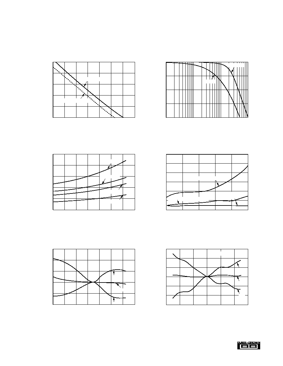
TYPICAL PERFORMANCE CURVES
At T
A
= 25
∞
C, V
S1
, V
S2
= 5.0V
DC
, V
IN
+, V
IN
≠ = 0V unless otherwise noted.
≠40
110
100
90
80
70
60
3dB Bandwidth (kHz)
BANDWIDTH vs TEMPERATURE
≠20
0
20
40
60
80
100
48
44
40
36
32
28
Temperature (∞C)
45∞ Phase Bandwidth (kHz)
3dB Bandwidth
45∞ Phase Bandwidth
AMPLITUDE and PHASE RESPONSE vs FREQUENCY
0
≠1
≠2
≠3
≠4
Relative Amplitude (dB)
100
1k
10k
100k
Frequency (Hz)
0
≠5
≠10
≠15
≠30
≠45
≠60
Phase (degrees)
Amplitude
Phase
≠40
10
8
6
4
2
0
Time (µs)
PROPAGATION DELAYS and RISE/FALL TIME
vs TEMPERATURE
≠20
0
20
40
60
80
100
Temperature (∞C)
Delay to 90%
Rise/Fall Time
Delay to 10%
Delay to 50%
≠40
1500
1000
500
0
≠500
≠1000
Input Offset Voltage Change (µV)
INPUT OFFSET VOLTAGE CHANGE vs TEMPERATURE
≠20
0
20
40
60
80
100
Temperature (∞C)
+2
≠2
Mean
4.4
600
400
200
0
≠200
≠400
≠600
Input Offset Voltage Change (µV)
INPUT OFFSET VOLTAGE CHANGE vs
INPUT SUPPLY VOLTAGE
Input Supply Voltage, V
S1
(V)
4.6
4.8
5.0
5.2
5.4
5.6
+2
Mean
≠2
V
S2
= 5V
0
3
2.5
2
1.5
1
0.5
0
Input Voltage Noise (mVrms)
INPUT VOLTAGE NOISE vs INPUT VOLTAGE
50
100
150
Input Voltage (mV)
200
250
No Bandwidth Limiting
Bandwidth Limited to 100kHz
Bandwidth Limited
to 10kHz