 | ÐлекÑÑоннÑй компоненÑ: ISO809P | СкаÑаÑÑ:  PDF PDF  ZIP ZIP |
Äîêóìåíòàöèÿ è îïèñàíèÿ www.docs.chipfind.ru
Isolated 16-Bit Sampling
ANALOG-TO-DIGITAL CONVERTER
ISO809
®
FEATURES
q
100kHz SAMPLING RATE
q
1500Vrms ISOLATION CONTINUOUS
q
10
µ
S CONVERSION TIME
q
16-BIT SERIAL OUTPUT
q
SINGLE +5V SUPPLY
q
28-PIN 0.6" PLASTIC DIP
APPLICATIONS
q
INDUSTRIAL PROCESS CONTROL
q
PC-BASED DATA ACQUISITION TEST
EQUIPMENT
DESCRIPTION
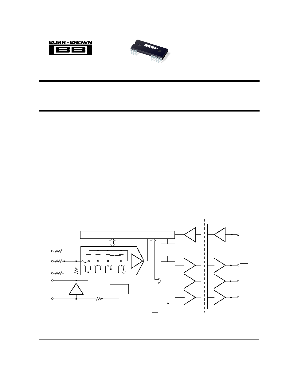
The ISO809 is a low-power isolated sampling ADC
using state-of-the-art CMOS structures and high volt-
age capacitors. The ISO809 contains a complete 16-bit
capacitor based SAR, ADC with S/H, clock, refer-
ence,
µ
P interface, serial out and galvanic isolation.
Laser-trimmed scaling resistors provide standard
industrial input ranges including
±
10V,
±
5V, 0-5V,
0-4V. They are available in 28-pin 0.6" wide plastic
DIP and are specified over the industrial temperature
range of 40
°
C to +85
°
C.
©
1996 Burr-Brown Corporation
PDS-1321B
Printed in U.S.A. August, 1997
ISO809
10k
4k
20k
5k
Internal
+2.5V Ref
Successive Approximation Register and Control Logic
Serial
Data
Out
Clock
Isolation
Barrier
20k
R1
IN
R2
IN
R3
IN
REF
CAP
BUSY
R/C
Data Clock
Serial Data
SB/BTC
International Airport Industrial Park · Mailing Address: PO Box 11400, Tucson, AZ 85734 · Street Address: 6730 S. Tucson Blvd., Tucson, AZ 85706 · Tel: (520) 746-1111 · Twx: 910-952-1111
Internet: http://www.burr-brown.com/ · FAXLine: (800) 548-6133 (US/Canada Only) · Cable: BBRCORP · Telex: 066-6491 · FAX: (520) 889-1510 · Immediate Product Info: (800) 548-6132
2
®
ISO809
SPECIFICATIONS
ELECTRICAL
At T
A
= 40
°
C to +85
°
C, f
S
= 100kHz, V
DIG
= V
ANA
= +5V, using internal reference and fixed resistors shown in Figure 3, unless otherwise specified.
ISO809P
PARAMETER
CONDITIONS
MIN
TYP
MAX
UNITS
The information provided herein is believed to be reliable; however, BURR-BROWN assumes no responsibility for inaccuracies or omissions. BURR-BROWN
assumes no responsibility for the use of this information, and all use of such information shall be entirely at the user's own risk. Prices and specifications are subject
to change without notice. No patent rights or licenses to any of the circuits described herein are implied or granted to any third party. BURR-BROWN does not
authorize or warrant any BURR-BROWN product for use in life support devices and/or systems.
ISOLATION PARAMETERS
Rated Voltage, Continuous
50Hz
1500
Vrms
Partial Discharge, 100% Test
(8)
1s, 5pC
2500
Vrms
Creepage Distance (External) DIP = "P" Package
16
mm
Internal Isolation Distance
0.10
mm
Barrier Impedance
>10
13
II 15
II pF
Leakage Current
(9)
240Vrms, 60Hz
1.2
µ
Arms
240Vrms, 50Hz
1.0
µ
Arms
RESOLUTION
16
Bits
ANALOG INPUT
Voltage Ranges
±
10V, 0V to 5V, etc. (See Table I)
Impedance
See Table I
Capacitance
35
pF
THROUGHPUT SPEED
Conversion Time
7.6
8
µ
s
Complete Cycle
Acquire and Convert
10
µ
s
Throughput Rate
100
kHz
DC ACCURACY
Integral Linearity Error
±
4
LSB
(1)
Differential Linearity Error
±
4
LSB
No Missing Codes
15
Transition Noise
(2)
1.3
LSB
Full Scale Error
(3,4)
±
0.5
%
Full Scale Error Drift
±
7
ppm/
°
C
Full Scale Error Drift
Ext. 2.5000V Ref
±
2
ppm/
°
C
Bipolar Zero Error
(3)
Bipolar Ranges
±
10
mV
Bipolar Zero Error Drift
Bipolar Ranges
±
2
ppm/
°
C
Unipolar Zero Error
(3)
Unipolar Ranges
3
mV
Unipolar Zero Error Drift
Unipolar Ranges
±
2
ppm/
°
C
Power Supply Sensitivity (V
DIG
= V
ANA
= V
D
)
+4.75V < V
D
< +5.25V
8
LSB
AC ACCURACY
Spurious-Free Dynamic Range
f
IN
= 45kHz
±
10V
100
dB
(5)
Total Harmonic Distortion
f
IN
= 45kHz
±
10V
100
dB
Signal-to-(Noise+Distortion)
f
IN
= 45kHz
±
10V
88
dB
Signal-to-Noise
f
IN
= 45kHz
±
10V
88
dB
Full-Power Bandwidth
(6)
250
kHz
SAMPLING DYNAMICS
Aperture Delay
40
ns
Aperture Jitter
Sufficient to meet AC specs
ns
Overvoltage Recovery
(7)
150
ns
REFERENCE
Internal Reference Voltage
No Load
2.48
2.5
2.52
V
Internal Reference Source Current
1
µ
A
(Must use external buffer)
External Reference Voltage Range
2.3
2.5
2.7
V
for Specified Linearity
External Reference Current Drain
Ext. 2.5000V Ref
100
µ
A
DIGITAL INPUTS
Logic Levels
V
IL
0.3
1.0
V
V
IH
V
D
1.0
V
D
+0.3V
V
I
IL
V
IL
= 0V
±
10
µ
A
I
IH
V
IH
= 5V
±
10
µ
A
DIGITAL OUTPUTS
Data Coding
Binary Two's Complement or Straight Binary
V
OL
I
SINK
= 1.6mA
±
0.4
V
V
OH
I
SOURCE
= 500
µ
A
+4
V
3
®
ISO809
POWER SUPPLIES
Specified Performance
V
DIG1
Must be
V
ANA
+4.75
+5
+5.25
V
V
ANA
+4.75
+5
+5.25
V
V
DIG2
+4.75
+5.25
V
I
DIG1
4.2
mA
I
ANA
21
mA
I
DIG2
10.8
mA
Power Dissipation
V
ANA
= V
DIG
= 5V, f
S
= 100kHz
175
mW
TEMPERATURE RANGE
Specified Performance
40
+85
°
C
Storage
65
+150
°
C
Thermal Resistance,
JA
Plastic DIP
75
°
C/W
SPECIFICATIONS
(CONT)
ELECTRICAL
At T
A
= 40
°
C to +85
°
C, f
S
= 100kHz, V
DIG
= V
ANA
= +5V, using internal reference and fixed resistors shown in Figure 3, unless otherwise specified.
ISO809P
PARAMETER
CONDITIONS
MIN
TYP
MAX
UNITS
NOTES: (1) LSB means Least Significant Bit. One LSB for the
±
10V input range is 3.05
µ
V. (2) Typical rms noise at worst case transition. (3) As measured with
fixed resistors shown in Figure 7b. Adjustable to zero with external potentiometer. (4) Full scale error is the worst case of Full Scale or +Full Scale untrimmed
deviation from ideal first and last code transitions, divided by the transition voltage (not divided by the full-scale range) and includes the effect of offset error. (5)
All specifications in dB are referred to a full-scale input. (6) Usable Bandwidth defined as Full-Scale input frequency at which Signal-to-(Noise + Distortion) degrades
to 60dB. (7) Recovers to specified performance after 2 x FS input overvoltage. (8) All devices receive a 1s test. Failure criterion is
5 pulses of
5pC. (9) Tested
at 2500Vrms, 50Hz limit 10
µ
A.
ELECTROSTATIC
DISCHARGE SENSITIVITY
Electrostatic discharge can cause damage ranging from per-
formance degradation to complete device failure. Burr-
Brown Corporation recommends that all integrated circuits
be handled and stored using appropriate ESD protection
methods.
ESD damage can range from subtle performance degrada-
tion to complete device failure. Precision integrated circuits
may be more susceptible to damage because very small
parametric changes could cause the device not to meet
published specifications.
Analog Inputs: R1
IN
...........................................................................
±
25V
R2
IN
...........................................................................
±
25V
R3
IN
...........................................................................
±
25V
CAP .................................... V
ANA
+0.3V to AGND2 0.3V
REF ........................................... Indefinite Short to AGND,
Momentary Short to V
ANA
Ground Voltage Differences: DGND and AGND ...............................
±
0.3V
DGND, AGND, and GND
ISO ...........
1563Vrms
V
ANA
....................................................................................................... 7V
V
DIG
to V
ANA
...................................................................................... +0.3V
V
DIG
........................................................................................................ 7V
Digital Inputs .............................................................. 0.3V to V
DIG
+0.3V
Maximum Junction Temperature ................................................... +165
°
C
Internal Power Dissipation ............................................................. 700mW
Lead Temperature (soldering, 10s) ................................................ +300
°
C
ABSOLUTE MAXIMUM RATINGS
PACKAGE INFORMATION
PACKAGE DRAWING
PRODUCT
PACKAGE
NUMBER
(1)
ISO809P
28-Pin Plastic DIP
215-1
NOTE: (1) For detailed drawing and dimension table, please see end of data
sheet, or Appendix C of Burr-Brown IC Data Book.
MAXIMUM INTEGRAL
TYPICAL SIGNAL-TO-
SPECIFICATION
PRODUCT
LINEARITY ERROR (LSB)
(NOISE + DISTORTION) RATIO (dB)
TEMPERATURE RANGE (
°
C)
PACKAGE
ISO809P
±
4
83
40
°
C to +85
°
C
28-Pin Plastic DIP
ORDERING INFORMATION
4
®
ISO809
SYMBOL
DESCRIPTION
MIN
TYP MAX UNITS
t
1
Convert Pulse Width
40
4500
ns
t
2
BUSY Delay
120
ns
t
3
BUSY LOW
8
µ
s
t
4
BUSY Delay after
220
ns
End of Conversion
t
5
Aperture Delay
40
ns
t
6
Conversion Time
5.7
8
µ
s
t
7
Acquisition Time
2
µ
s
t
6
+ t
7
Throughput Time
9
10
µ
s
t
8
R/C LOW to DATACLK Delay
450
ns
t
9
DATACLK Period
440
ns
t
10
Data Valid to DATACLK
20
75
ns
HIGH Delay
t
11
Data Valid after
100
125
ns
DATACLK LOW Delay
DIGITAL
PIN #
NAME
I/O
DESCRIPTION
1
RC
I
Read/Convert. With BUSY high, a falling edge on R/C initiates a new conversion.
2
BUSY
O
At the start of conversion BUSY goes LOW and stays LOW until conversion is complete.
3
+5V
DIG2
Isolated Digital Supply Volts.
10
+5V
DIG1
Digital Supply Volts.
11
+5V
ANA
Analog Supply Volts.
12
R1
IN
Analog Input.
13
R2
N
Analog Input.
14
R3
N
Analog Input.
15
CAP
Reference Buffer Output. 2.2
µ
F tantalum capacitor to ground.
16
REF
Reference Input/Output. 2.2
µ
F tantalum capacitor to ground.
17
AGND
Analog Ground.
18
SB/BTC
I
Selects Straight Binary or Binary Two's Complement for output data format.
19
DGND1
Digital Ground.
26
DGND2
Isolated Ground.
27
DATACLK
O
Data Clock Output.
28
SDATA
O
Serial Output Synchronized to DATACLK.
TABLE I. Pin Assignments.
PIN CONFIGURATION
ANALOG
CONNECT R1
IN
CONNECT R2
IN
INPUT
VIA 200
VIA 100
CONNECT R3
IN
RANGE
TO
TO
TO
IMPEDANCE
±
10V
V
IN
AGND
CAP
22.9k
±
5V
AGND
V
IN
CAP
13.3k
±
3.33
V
IN
V
IN
CAP
10.7k
0V to 10V
AGND
V
IN
AGND
13.3k
0V to 5V
AGND
AGND
V
IN
10.0k
0V to 4V
V
IN
AGND
V
IN
10.7k
TABLE I. Input Range Connections. See Figure 3 for
complete information.
TABLE II. Conversion and Data Timing. T
A
= 40
°
C to +85
°
C.
SDATA
DATACLK
DGND2
DGND1
SB/BTC
AGND
REF
CAP
R/C
BUSY
+5V
DIG2
+5V
DIG1
+5V
ANA
R1
IN
R2
IN
R3
IN
1
2
3
10
11
12
13
14
28
27
26
19
18
17
16
15
ISO809
5
®
ISO809
1
MSB Valid
R/C
DATACLK
SDATA
t
8
t
11
t
10
t
9
2
3
15
16
Bit 14 Valid
Bit 1 Valid
Bit 13 Valid
LSB Valid
t
2
t
3
BUSY
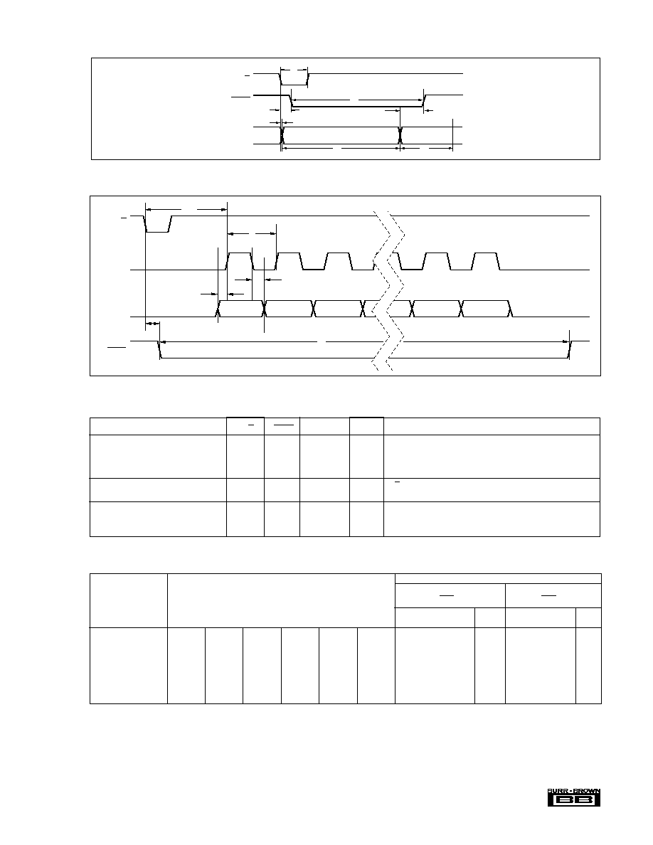
FIGURE 1. Basic Conversion Timing.
MODE Acquire
t
4
t
5
t
1
t
3
t
7
t
6
Convert
Acquire
t
2
BUSY
R/C
FIGURE 2. Serial Data Timing.
SPECIFIC FUNCTION
R/C
BUSY
DATACLK
SB/BTC
OPERATION
TABLE III. Control Truth Table.
Initiate Conversion and Output Data
0
1
Output
X
Initiates Conversion "n". Data from conversion "n1" clocked out
on DATA synchronized to 12 clock pulses output on DATACLK.
1 > 0
1
Output
X
Initiates Conversion "n". Data from conversion "n1" clocked out
on DATA synchronized to 12 clock pulses output on DATACLK.
Incorrect Conversions
0
0 > 1
X
X
R/C must be HIGH or a new conversion will be initiated without
time for acquisition.
Selecting Output Format
X
X
X
0
Serial Data is output in Binary Two's Complement format.
X
X
X
1
Serial Data is output in Straight Binary format.
ANALOG INPUT
BINARY TWO'S COMPLEMENT
STRAIGHT BINARY
(SB/BTC LOW)
(SB/BTC HIGH)
DIGITAL OUTPUT
TABLE IV. Output Codes and Ideal Input Voltages.
HEX
HEX
DESCRIPTION
BINARY CODE
CODE
BINARY CODE
CODE
Full-Scale Range
±
10
±
5
±
3.33V
0V to 10V
0V to 5V
0V to 4V
Least Significant Bit (LSB)
305
µ
V
153
µ
V
102
µ
V
153
µ
V
76
µ
V
61
µ
V
+Full Scale (FS 1LSB)
9.999695V
4.999847V 3.333231V
9.999847V 4.999924V 3.999939V
0111 1111 1111 1111
7FFF
1111 1111 1111 1111
FFFF
Midscale
0V
0V
0V
5V
2.5V
2V
0000 0000 0000 0000
0000
1000 0000 0000 0000
8000
One LSB Below Midscale
305
µ
V
153
µ
V
102
µ
V
4.999847V 2.499924V 1.999939V
1111 1111 1111 1111
FFFF
0111 1111 1111 1111
7FFF
Full Scale
10V
5V
3.333333V
0V
0V
0V
1000 0000 0000 0000
8000
0000 0000 0000 0000
0000