 | –≠–ª–µ–∫—Ç—Ä–æ–Ω–Ω—ã–π –∫–æ–º–ø–æ–Ω–µ–Ω—Ç: IVC102U | –°–∫–∞—á–∞—Ç—å:  PDF PDF  ZIP ZIP |
1
Æ
IVC102
I
IN
V
B
1
2
3
4
5
6
11
12
13
Digital
Ground
Analog
Ground
Logic Low closes switches
9
10
14
V
O
V+
V≠
S
1
S
2
Ionization
Chamber
Photodiode
60pF
30pF
10pF
S
1
C
1
C
2
C
3
S
2
International
Airport
Industrial
Park
∑ Mailing Address: PO Box 11400
∑
Tucson,
AZ
85734
∑
Street
Address:
6730
S.
Tucson
Blvd.
∑
Tucson,
AZ
85706
Tel:
(520)
746-1111
∑
Twx:
910-952-1111
∑
Cable:
BBRCORP
∑
Telex:
066-6491
∑
FAX:
(520)
889-1510
∑
Immediate
Product
Info:
(800)
548-6132
Æ
PRECISION SWITCHED INTEGRATOR
TRANSIMPEDANCE AMPLIFIER
APPLICATIONS
q
PRECISION LOW CURRENT MEASUREMENT
q
PHOTODIODE MEASUREMENTS
q
IONIZATION CHAMBER MEASUREMENTS
q
CURRENT/CHARGE-OUTPUT SENSORS
q
LEAKAGE CURRENT MEASUREMENT
IVC102
FEATURES
q
ON-CHIP INTEGRATING CAPACITORS
q
GAIN PROGRAMMED BY TIMING
q
LOW INPUT BIAS CURRENT: 750fA max
q
LOW NOISE
q
LOW SWITCH CHARGE INJECTION
q
FAST PULSE INTEGRATION
q
LOW NONLINEARITY: 0.005% typ
q
14-PIN DIP, SO-14 SURFACE MOUNT
DESCRIPTION
The IVC102 is a precision integrating amplifier with
FET op amp, integrating capacitors, and low leakage
FET switches. It integrates low-level input current for
a user-determined period, storing the resulting voltage
on the integrating capacitor. The output voltage can be
held for accurate measurement. The IVC102 provides
a precision, lower noise alternative to conventional
transimpedance op amp circuits that require a very
high value feedback resistor.
The IVC102 is ideal for amplifying low-level sensor
currents from photodiodes and ionization chambers.
The input signal current can be positive or negative.
TTL/CMOS-compatible timing inputs control the inte-
gration period, hold and reset functions to set the
effective transimpedance gain and to reset (discharge)
the integrator capacitor.
Package options include 14-Pin plastic DIP and SO-14
surface-mount packages. Both are specified for the
≠40
∞
C to 85
∞
C industrial temperature range.
© 1996 Burr-Brown Corporation
PDS-1329A
Printed in U.S.A. June, 1996
0V
Hold
Integrate
Hold
Reset
Positive or Negative
Signal Integration
S
1
S
2
I
IN
(t)
V
O
=
≠1
dt
C
INT

2
Æ
IVC102
The information provided herein is believed to be reliable; however, BURR-BROWN assumes no responsibility for inaccuracies or omissions. BURR-BROWN assumes
no responsibility for the use of this information, and all use of such information shall be entirely at the user's own risk. Prices and specifications are subject to change
without notice. No patent rights or licenses to any of the circuits described herein are implied or granted to any third party. BURR-BROWN does not authorize or warrant
any BURR-BROWN product for use in life support devices and/or systems.
NOTES: (1) Standard test timing: 1ms integration, 200
µ
s hold, 100
µ
s reset. (2) Hold mode output voltage after 1ms integration of zero input current. Includes op
amp offset voltage, integration of input error current and switch charge injection effects.
SPECIFICATIONS
At T
A
= +25
∞
C, V
S
=
±
15V, R
L
= 2k
,
C
INT
= C
1
+ C
2
+ C
3
, 1ms integration period
(1)
, unless otherwise specified.
IVC102P, U
PARAMETER
CONDITIONS
MIN
TYP
MAX
UNITS
TRANSFER FUNCTION
V
O
= ≠(I
IN
)(T
INT
)/C
INT
Gain Error
C
INT
= C
1
+ C
2
+ C
3
±
5
+25/≠17
%
vs Temperature
±
25
ppm/
∞
C
Nonlinearity
V
O
=
±
10V
±
0.005
%
Input Current Range
±
100
µ
A
Offset Voltage
(2)
I
IN
= 0, C
IN
= 50pF
≠5
±
20
mV
vs Temperature
±
30
µ
V/
∞
C
vs Power Supply
V
S
= +4.75/≠10 to +18/≠18V
150
750
µ
V/V
Droop Rate, Hold Mode
≠1
nV/
µ
s
OP AMP
Input Bias Current
S
1
, S
2
Open
≠100
±
750
fA
vs Temperature
See Typical Curve
Offset Voltage (Op Amp V
OS
)
±
0.5
±
5
mV
vs Temperature
±
5
µ
V/
∞
C
vs Power Supply
V
S
= +4.75/≠10 to +18/≠18V
10
100
µ
V/V
Noise Voltage
f = 1kHz
10
nV/
Hz
INTEGRATION CAPACITORS
C
1
+ C
2
+ C
3
80
100
120
pF
vs Temperature
±
25
ppm/
∞
C
C
1
10
pF
C
2
30
pF
C
3
60
pF
OUTPUT
Voltage Range, Positive
R
L
= 2k
(V+)≠3
(V+)≠1.3
V
Negative
R
L
= 2k
(V≠)+3
(V≠)+2.6
V
Short-Circuit Current
±
20
mA
Capacitive Load Drive
500
pF
Noise Voltage
See Typical Curve
DYNAMIC CHARACTERISTIC
Op Amp Gain-Bandwidth
2
MHz
Op Amp Slew Rate
3
V/
µ
s
Reset
Slew Rate
3
V/
µ
s
Settling Time, 0.01%
10V Step
6
µ
s
DIGITAL INPUTS
(TTL/CMOS Compatible)
V
IH
(referred to digital ground)
(Logic High)
2
5.5
V
V
IL
(referred to digital ground)
(Logic Low)
≠0.5
0.8
V
I
IH
V
IH
= 5V
2
µ
A
I
IL
V
IL
= 0V
0
µ
A
Switching Time
100
ns
POWER SUPPLY
Voltage Range: Positive
+4.75
+15
+18
V
Negative
≠10
≠15
≠18
V
Current: Positive
4.1
5.5
mA
Negative
≠1.6
≠2.2
mA
Analog Ground
≠0.2
mA
Digital Ground
≠2.3
mA
TEMPERATURE RANGE
Operating Range
≠40
85
∞
C
Storage
≠55
125
∞
C
Thermal Resistance,
JA
DIP
100
∞
C/W
SO-14
150
∞
C/W

3
Æ
IVC102
ELECTROSTATIC
DISCHARGE SENSITIVITY
This integrated circuit can be damaged by ESD. Burr-Brown
recommends that all integrated circuits be handled with
appropriate precautions. Failure to observe proper handling
and installation procedures can cause damage.
ESD damage can range from subtle performance degrada-
tion to complete device failure. Precision integrated circuits
may be more susceptible to damage because very small
parametric changes could cause the device not to meet its
published specifications.
ABSOLUTE MAXIMUM RATINGS
Supply Voltage, V+ to V≠ .................................................................... 36V
Logic Input Voltage ...................................................................... V≠ to V+
Output Short Circuit to Ground ............................................... Continuous
Operating Temperature ................................................. ≠40
∞
C to +125
∞
C
Storage Temperature ..................................................... ≠55
∞
C to +125
∞
C
Lead Temperature (soldering, 10s) ................................................. 300
∞
C
PIN CONNECTIONS
Top View
14-Pin DIP/
SO-14 Surface Mount
PACKAGE INFORMATION
PACKAGE DRAWING
PRODUCT
PACKAGE
NUMBER
(1)
IVC102P
14-Pin DIP
010
IVC102U
SO-14 Surface Mount
235
NOTE: (1) For detailed drawing and dimension table, please see end of data
sheet, or Appendix D of Burr-Brown IC Data Book.
V+
Digital Ground
S
2
S
1
V
O
V≠
NC
Analog Ground
I
IN
≠In
C
1
C
2
C
3
NC
NC = No Internal Connection
Connect to Analog Ground for Lowest Noise
14
13
12
11
10
9
8
1
2
3
4
5
6
7

4
Æ
IVC102
10
100
1000
C
IN
(pF)
TOTAL OUTPUT NOISE vs C
IN
1000
100
10
1
Noise Voltage (µVrms)
rms Variation
of 100 Measurement
Cycles, T
INT
= 1ms.
C
INT
= 10pF
C
INT
= 30pF
C
INT
= 100pF
C
INT
= 300pF
C
INT
= 1000pF
Reset Mode, S
1
Open, S
2
Closed.
TYPICAL PERFORMANCE CURVES
At T
A
= +25
∞
C, V
S
=
±
15V, R
L
= 2k
,
C
INT
= C
1
+ C
2
+ C
3
, 1ms integration period, unless otherwise specified.
≠50
≠25
0
25
50
75
100
125
Temperature (∞C)
INPUT BIAS CURRENT vs TEMPERATURE
100p
10p
1p
100f
10f
Input Bias Current (A)
S
1
, S
2
Open
0
100
200
300
400
500
600
700
800
900 1000
C
INT
(pF)
RESET TIME vs C
INT
30
25
20
15
10
5
0
Reset Time (µs)
Time Required to
Reset from ±10V
to 0V.
0.01%
1%
10
100
1000
Input Capacitance, C
IN
(pF)
S
1
CHARGE INJECTION vs INPUT CAPACITANCE
2.0
1.8
1.6
1.4
1.2
1.0
0.8
0.6
0.4
0.2
0
Charge Injection,
Q (pC)
100pF
V
O
=
Q
100pF
S
1
C
IN
10
100
1000
Input Capacitance, C
IN
(pF)
S
2
CHARGE INJECTION vs INPUT CAPACITANCE
1.0
0.9
0.8
0.7
0.6
0.5
0.4
0.3
0.2
0.1
0
Charge Injection,
Q (pC)
(V+) = +18V
(V+) = +15V
(V+) = +4.75V
100pF
V
O
=
Q
100pF
C
IN
S
2

5
Æ
IVC102
Charge Injection
of S
2
Op Amp V
OS
+
I
IN
∑ R
S2
0V
Integrate
(S
2
Open)
T
1
0V
S
2
V
O
T
2
10µs
Reset
10µs
Reset
I
IN
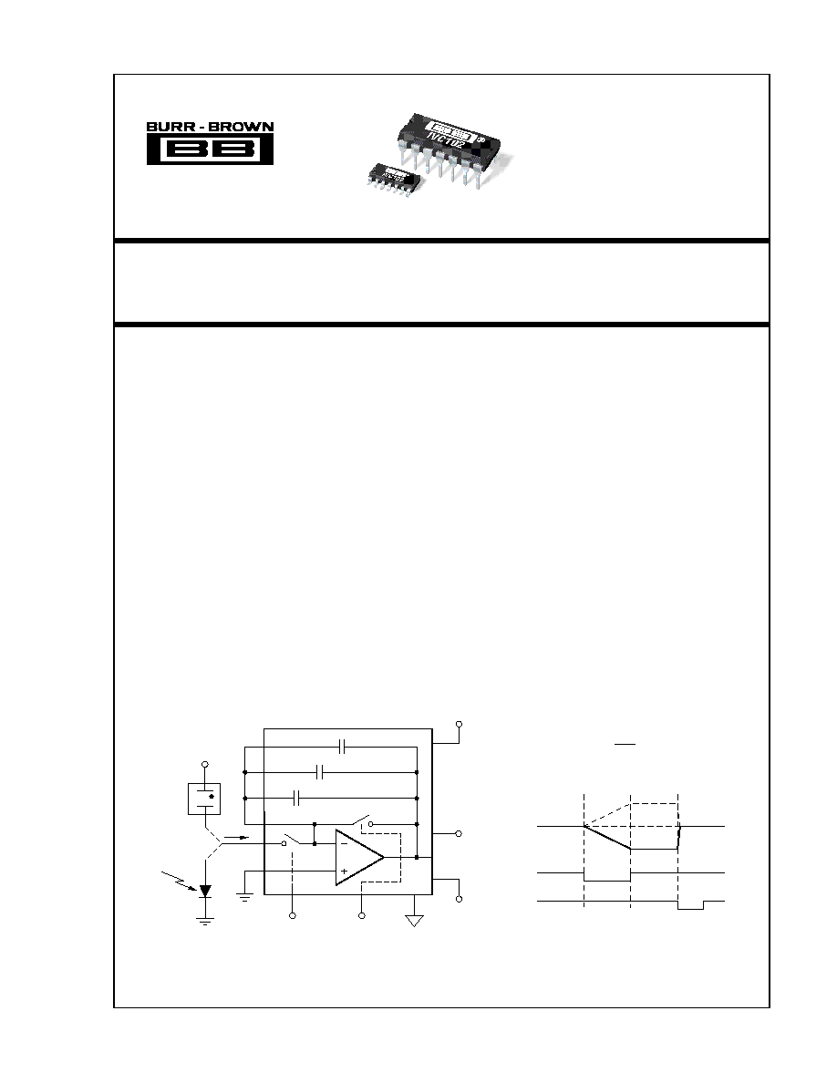
Photodiode
60pF
30pF
10pF
0.1µF
0.1µF
1
2
3
4
5
6
11
12
13
10
V
O
14
V+
+15V
Logic
High
(+5V)
S
1
C
1
C
2
C
3
S
2
Digital
Ground
Analog
Ground
S
2
9
≠15V
V≠
Digital
Data
Sampling
A/D
Converter
See timing
signal below
APPLICATION INFORMATION
Figure 1 shows the basic circuit connections to operate the
IVC102. Bypass capacitors are shown connected to the
power supply pins. Noisy power supplies should be avoided
or decoupled and carefully bypassed.
The Analog Ground terminal, pin 1, is shown internally
connected to the non-inverting input of the op amp. This
terminal connects to other internal circuitry and should be
connected to ground. Approximately 200
µ
A flows out of
this terminal.
Digital Ground, pin 13, should be at the same voltage
potential as analog ground (within 100mV). Analog and
Digital grounds should be connected at some point in the
system, usually at the power supply connections to the
circuit board. A separate Digital Ground is provided so that
noisy logic signals can be referenced to separate circuit
board traces.
Integrator capacitors C
1
, C
2
and C
3
are shown connected in
parallel for a total C
INT
= 100pF. The IVC102 can be used
for a wide variety of integrating current measurements. The
input signal connections and control timing and C
INT
value
will depend on the sensor or signal type and other applica-
tion details.
BASIC RESET-AND-INTEGRATE MEASUREMENT
Figure 1 shows the circuit and timing for a simple reset-and-
integrate measurement. The input current is connected di-
rectly to the inverting input of the IVC102, pin 3. Input
current is shown flowing out of pin 3, which produces a
positive-going ramp at V
O
. Current flowing into pin 3 would
produce a negative-going ramp.
A measurement cycle starts by resetting the integrator output
voltage to 0V by closing S
2
for 10
µ
s. Integration of the input
current begins when S
2
opens and the input current begins to
charge C
INT
. V
O
is measured with a sampling a/d converter
at the end of an integration period, just prior to the next reset
period. The ideal result is proportional to the average input
current (or total accumulated charge).
Switch S
2
is again closed to reset the integrator output to 0V
before the next integration period.
This simple measurement arrangement is suited to many
applications. There are, however, limitations to this basic
approach. Input current continues to flow through S
2
during
the reset period. This leaves a small voltage on C
INT
equal
to the input current times R
S2
, the on-resistance of S
2
,
approximately 1.5k
.
FIGURE 1. Reset-and Integrate Connections and Timing.
Figure 1b
Figure 1a