 | –≠–ª–µ–∫—Ç—Ä–æ–Ω–Ω—ã–π –∫–æ–º–ø–æ–Ω–µ–Ω—Ç: LOG101AID | –°–∫–∞—á–∞—Ç—å:  PDF PDF  ZIP ZIP |
FEATURES
q
EASY-TO-USE COMPLETE CORE FUNCTION
q
HIGH ACCURACY: 0.01% FSO Over 5 Decades
q
WIDE INPUT DYNAMIC RANGE:
7.5 Decades, 100pA to 3.5mA
q
LOW QUIESCENT CURRENT: 1mA
q
WIDE SUPPLY RANGE:
±
4.5V to
±
18V
Precision
LOGARITHMIC AND LOG RATIO AMPLIFIER
DESCRIPTION
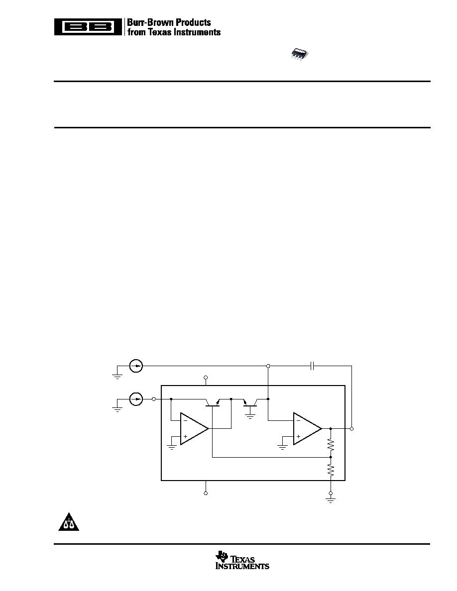
The LOG101
is a versatile integrated circuit that computes
the logarithm or log ratio of an input current relative to a
reference current.
The LOG101 is tested over a wide dynamic range of input
signals. In log ratio applications, a signal current can come
from a photodiode, and a reference current from a resistor in
series with a precision external reference.
The output signal at V
OUT
is trimmed to 1V per decade of input
current allowing seven decades of input current dynamic
range.
Low DC offset voltage and temperature drift allow accurate
measurement of low-level signals over a wide environmental
temperature range. The LOG101 is specified over the tem-
perature range ≠5
∞
C to +75
∞
C, with operation over
≠40
∞
C to +85
∞
C.
APPLICATIONS
q
LOG, LOG RATIO COMPUTATION:
Communication, Analytical, Medical, Industrial,
Test, and General Instrumentation
q
PHOTODIODE SIGNAL COMPRESSION AMPS
q
ANALOG SIGNAL COMPRESSION IN FRONT
OF ANALOG-TO-DIGITAL (A/D) CONVERTERS
LOG101
www.ti.com
PRODUCTION DATA information is current as of publication date.
Products conform to specifications per the terms of Texas Instruments
standard warranty. Production processing does not necessarily include
testing of all parameters.
Copyright © 2002-2004, Texas Instruments Incorporated
SBOS242B ≠ MAY 2002 ≠ REVISED JUNE 2004
Please be aware that an important notice concerning availability, standard warranty, and use in critical applications of
Texas Instruments semiconductor products and disclaimers thereto appears at the end of this data sheet.
Note: Protected under US Patent #6,667,650; other patents pending.
A
2
A
1
1
5
8
4
6
3
Q
1
Q
2
C
C
I
2
I
1
R
1
R
2
V≠
V
OUT
V+
GND
LOG101
V
OUT
= (1V) ∑ LOG (I
1
/I
2
)
LOG1
01
All trademarks are the property of their respective owners.
www.ti.com
LOG101
2
SBOS242B
SPECIFIED
PACKAGE
TEMPERATURE
PACKAGE
ORDERING
TRANSPORT
PRODUCT
PACKAGE-LEAD
DESIGNATOR
RANGE
MARKING
NUMBER
MEDIA, QUANTITY
LOG101AID
SO -8
D
≠5
∞
C to +75
∞
C
LOG101
LOG101AID
Rails, 100
"
"
"
"
"
LOG101AIDR
Tape and Reel, 2500
NOTE: (1) For the most current package and ordering information, see the Package Option Addendum located at the end of this data sheet.
ELECTROSTATIC
DISCHARGE SENSITIVITY
This integrated circuit can be damaged by ESD. Texas Instru-
ments recommends that all integrated circuits be handled with
appropriate precautions. Failure to observe proper handling
and installation procedures can cause damage.
ESD damage can range from subtle performance degrada-
tion to complete device failure. Precision integrated circuits
may be more susceptible to damage because very small
parametric changes could cause the device not to meet its
published specifications.
ABSOLUTE MAXIMUM RATINGS
(1)
Supply Voltage, V+ to V≠ .................................................................... 36V
Input Voltage .................................................... (V≠) ≠ 0.5 to (V+) + 0.5V
Input Current ...................................................................................
±
10mA
Output Short-Circuit
(2)
.............................................................. Continuous
Operating Temperature .................................................... ≠40
∞
C to +85
∞
C
Storage Temperature ..................................................... ≠55
∞
C to +125
∞
C
Junction Temperature .................................................................... +150
∞
C
Lead Temperature (soldering, 10s) ............................................... +300
∞
C
NOTES: (1) Stresses above these ratings may cause permanent damage.
Exposure to absolute maximum conditions for extended periods may degrade
device reliability. (2) Short-circuit to ground.
PACKAGE/ORDERING INFORMATION
(1)
PIN DESCRIPTION
ELECTRICAL CHARACTERISTICS
Boldface limits apply over the specified temperature range, T
A
= ≠5
∞
C to +75
∞
C.
At T
A
= +25
∞
C, V
S
=
±
5V, and R
OUT
= 10k
, unless otherwise noted.
Top View
SO
I
2
NC
GND
V≠
NC = No Internal Connection
LOG101
I
1
NC
V
OUT
V+
8
7
6
5
1
2
3
4
LOG101AID
PARAMETER
CONDITION
MIN
TYP
MAX
UNITS
CORE LOG FUNCTION
I
IN
/ V
OUT
Equation
V
O
= (1V) ∑ log (I
1
/I
2
)
V
LOG CONFORMITY ERROR
(1)
Initial
1nA to 100
µ
A (5 decades)
0.01
0.2
%
100pA to 3.5mA (7.5 decades)
0.06
%
over Temperature
1nA to 100
µ
A (5 decades)
0.0001
%/
∞
C
100pA to 3.5mA (7.5 decades)
(2)
0.0005
%/
∞
C
GAIN
(3)
Initial Value
1nA to 100
µ
A
1
V/decade
Gain Error
1nA to 100
µ
A
0.15
±
1
%
vs Temperature
T
MIN
to T
MAX
0.003
0.01
%/
∞
C
INPUT, A1 and A2
Offset Voltage
±
0.3
±
1.5
mV
vs Temperature
T
MIN
to T
MAX
±
2
µ
V/
∞
C
vs Power Supply (PSRR)
V
S
=
±
4.5V to
±
18V
5
50
µ
V/V
Input Bias Current
±
5
pA
vs Temperature
T
MIN
to T
MAX
Doubles Every 10
∞
C
Voltage Noise
f = 10Hz to 10kHz
3
µ
Vrms
f = 1kHz
30
nV/
Hz
Current Noise
f = 1kHz
4
fA/
Hz
Common-Mode Voltage Range (Positive)
(V+) ≠ 2
(V+) ≠ 1.5
V
(Negative)
(V≠) + 2
(V≠) + 1.2
V
Common-Mode Rejection Ratio (CMRR)
105
dB
OUTPUT, A2 (V
OUT
)
Output Offset, V
OSO
, Initial
±
3
±
15
mV
vs Temperature
T
MIN
to T
MAX
±
2
µ
V/
∞
C
Full-Scale Output (FSO)
V
S
=
±
5V
(V≠) + 1.2
(V+) ≠ 1.5
V
Short-Circuit Current
±
18
mA

www.ti.com
LOG101
3
SBOS242B
TOTAL ERROR
(4)(5)
I
1
or I
2
remains fixed while other varies.
Initial
Min to Max
I
1
or I
2
= 3.5mA
±
75
mV
I
1
or I
2
= 1mA
±
20
mV
I
1
or I
2
= 100
µ
A
±
20
mV
I
1
or I
2
= 10
µ
A
±
20
mV
I
1
or I
2
= 1
µ
A
±
20
mV
I
1
or I
2
= 100nA
±
20
mV
I
1
or I
2
= 10nA
±
20
mV
I
1
or I
2
= 1nA
±
20
mV
I
1
or I
2
= 350pA
±
20
mV
I
1
or I
2
= 100pA
±
20
mV
vs Temperature
I
1
or I
2
= 3.5mA
±
1.2
mV/
∞
C
I
1
or I
2
= 1mA
±
0.4
mV/
∞
C
I
1
or I
2
= 100
µ
A
±
0.1
mV/
∞
C
I
1
or I
2
= 10
µ
A
±
0.05
mV/
∞
C
I
1
or I
2
= 1
µ
A
±
0.05
mV/
∞
C
I
1
or I
2
= 100nA
±
0.09
mV/
∞
C
I
1
or I
2
= 10nA
±
0.2
mV/
∞
C
I
1
or I
2
= 1nA
±
0.3
mV/
∞
C
I
1
or I
2
= 350pA
±
0.1
mV/
∞
C
I
1
or I
2
= 100pA
±
0.3
mV/
∞
C
vs Supply
I
1
or I
2
= 3.5mA
±
3.0
mV/ V
I
1
or I
2
= 1mA
±
0.1
mV/ V
I
1
or I
2
= 100
µ
A
±
0.1
mV/ V
I
1
or I
2
= 10
µ
A
±
0.1
mV/ V
I
1
or I
2
= 1
µ
A
±
0.1
mV/ V
I
1
or I
2
= 100nA
±
0.1
mV/ V
I
1
or I
2
= 10nA
±
0.1
mV/ V
I
1
or I
2
= 1nA
±
0.25
mV/V
I
1
or I
2
= 350pA
±
0.1
mV/ V
I
1
or I
2
= 100pA
±
0.1
mV/ V
FREQUENCY RESPONSE, CORE LOG
(6)
BW, 3dB
I
2
= 10nA
C
C
= 4500pF
0.1
kHz
I
2
= 1
µ
A
C
C
= 150pF
38
kHz
I
2
= 10
µ
A
C
C
= 150pF
40
kHz
I
2
= 1mA
C
C
= 50pF
45
kHz
Step Response
Increasing
I
2
= 1
µ
A to 1mA
C
C
= 150pF
11
µ
s
I
2
= 100nA to 1
µ
A
C
C
= 150pF
7
µ
s
I
2
= 10nA to 100nA
C
C
= 150pF
110
µ
s
Decreasing
I
2
= 1mA to 1
µ
A
C
C
= 150pF
45
µ
s
I
2
= 1
µ
A to 100nA
C
C
= 150pF
20
µ
s
I
2
= 100nA to 10nA
C
C
= 150pF
550
µ
s
POWER SUPPLY
Operating Range
V
S
±
4.5
±
18
V
Quiescent Current
I
O
= 0
±
1
±
1.5
mA
TEMPERATURE RANGE
Specified Range, T
MIN
to T
MAX
≠5
75
∞
C
Operating Range
≠40
85
∞
C
Storage Range
≠55
125
∞
C
Thermal Resistance,
JA
SO-8
150
∞
C/W
NOTES: (1) Log Conformity Error is peak deviation from the best-fit straight line of V
OUT
versus log (I
1
/ I
2
) curve expressed as a percent of peak-to-peak full-scale.
(2) May require higher supply for full dynamic range.
(3) Output core log function is trimmed to 1V output per decade change of input current.
(4) Worst-case Total Error for any ratio of I
1
/I
2
is the largest of the two errors, when I
1
and I
2
are considered separately.
(5) Total I
1
+ I
2
should be kept below 4.5mA on
±
5V supply.
(6) Bandwidth (3dB) and transient response are a function of both the compensation capacitor and the level of input current.
ELECTRICAL CHARACTERISTICS
(Cont.)
Boldface limits apply over the specified temperature range, T
A
= ≠5
∞
C to +75
∞
C.
At T
A
= +25
∞
C, V
S
=
±
5V, and R
L
= 10k
, unless otherwise noted.
LOG101AID
PARAMETER
CONDITION
MIN
TYP
MAX
UNITS

www.ti.com
LOG101
4
SBOS242B
TYPICAL CHARACTERISTICS
At T
A
= +25
∞
C, V
S
=
±
5V, and R
L
= 10k
, unless otherwise noted.
0
ONE CYCLE OF NORMALIZED TRANSFER FUNCTION
Normalized Output Voltage (V)
1
0.9
0.8
0.7
0.6
0.5
0.4
0.3
0.2
0.1
2
6
1
10
3
Current Ratio, I
1
/I
2
4
8
4.0
3.0
2.0
1.0
0.0
≠1.0
≠2.0
≠3.0
≠4.0
Normalized Output V
oltage (V)
NORMALIZED TRANSFER FUNCTION
0.0001 0.001
0.01
0.1
1
10
100
1k
10k
Current Ratio, I
1
/I
2
V
OUT
= 1V LOG (I
1
/I
2
)
3dB FREQUENCY RESPONSE
3dB Frequency Response (Hz)
0.1
1M
100k
10k
1k
100
10
1
100
µ
A
100
µ
A
1mA
I
1
= 1mA
1
µ
A
1mA
to 10
µ
A
100nA
10nA
I
1
= 1nA
10nA
C
C
= 1000pF
C
C
= 1
µ
F
10
µ
A to 1
µ
A
C
C
= 1
0p
F
1nA
100
µ
A
100pA
1nA
10nA
100nA
1
µ
A
10
µ
A
100
µ
A
1mA
I
2
1
µ
A
10
µ
A
100
µ
A
I
1
= 1nA
10nA
120
100
80
60
40
20
0
100pA 1nA
10nA 100nA
1
µ
A
10
µ
A 100
µ
A 1mA 10mA
TOTAL ERROR vs INPUT CURRENT
Input Current (I
1
or I
2
)
T
otal Error (mV)
+75
∞
C
+25
∞
C
≠5
∞
C
5.8
4.8
3.8
2.8
1.8
0.8
≠0.2
100pA 1nA
10nA 100nA 1
µ
A
10
µ
A 100
µ
A 1mA
10mA
GAIN ERROR (I
2
= 1
µ
A)
Input Current (I
1
or I
2
)
Gain Error (%)
≠5
∞
C to ≠40
∞
C
+85
∞
C
+75
∞
C
+25
∞
C
MINIMUM VALUE OF COMPENSATION CAPACITOR
100M
10M
1M
100k
10k
1k
100
10
1
C
C
(pF)
100pA
1nA
10nA 100nA
1
µ
A
10
µ
A 100
µ
A 1mA 10mA
I
2
I
1
= 100pA
I
1
= 1nA
I
1
= 10nA
I
1
= 100nA
1
µ
A
I
1
= 10
µ
A
100
µ
A
1mA
Select C
C
for I
1
min.
and I
2
max. Values
below 2pF may be ignored.

www.ti.com
LOG101
5
SBOS242B
TYPICAL CHARACTERISTICS
(Cont.)
At T
A
= +25
∞
C, V
S
=
±
5V, and R
L
= 10k
, unless otherwise noted.
17
15
13
11
9
7
5
3
1
≠1
Input Current (I
1
or I
2
)
Log Conformity (mV)
LOG CONFORMITY vs INPUT CURRENT
+85
∞
C
+75
∞
C
≠40
∞
C to +25
∞
C
100pA
1nA
10nA
100nA
1
µ
A
10
µ
A
100
µ
A
1mA
LOG CONFORMITY vs TEMPERATURE
Log Conformity (m%)
350
300
250
200
150
100
50
0
≠40 ≠30 ≠20 ≠10 0
10 20
30 40
50 60
70 80
90
Temperature (
∞
C)
7 Decades
(100pA to 1mA)
6 Decades
(1nA to 1mA)
5 Decades
(1nA to 100
µ
A)
8
1
6
3
4
5
V≠
V+
10
µ
F
LOG101
1000pF
10
µ
F
1000pF
I
1
I
2
V
OUT
C
C
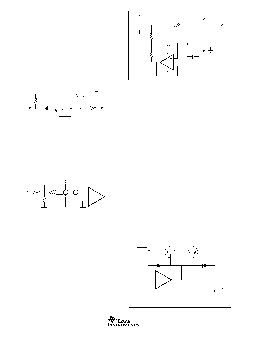
FIGURE 1. Basic Connections of the LOG101.
APPLICATION INFORMATION
The LOG101 is a true logarithmic amplifier that uses the
base-emitter voltage relationship of bipolar transistors to
compute the logarithm, or logarithmic ratio of a current ratio.
Figure 1 shows the basic connections required for operation
of the LOG101. In order to reduce the influence of lead
inductance of power-supply lines, it is recommended that
each supply be bypassed with a 10
µ
F tantalum capacitor in
parallel with a 1000pF ceramic capacitor, as shown in
Figure 1. Connecting the capacitors as close to the LOG101
as possible will contribute to noise reduction as well.
INPUT CURRENT RANGE
To maintain specified accuracy, the input current range of the
LOG101 should be limited from 100pA to 3.5mA. Input currents
outside of this range may compromise LOG101 performance.
Input currents larger than 3.5mA result in increased
nonlinearity. An absolute maximum input current rating of
10mA is included to prevent excessive power dissipation that
may damage the logging transistor.
On
±
5V supplies, the total input current (I
1
+ I
2
) is limited to
4.5mA. Due to compliance issues internal to the LOG101, to
accommodate larger total input currents, supplies should be
increased.
Currents smaller than 100pA will result in increased errors due
to the input bias currents of op amps A
1
and A
2
(typically 5pA).
The input bias currents may be compensated for, as shown in
Figure 2. The input stages of the amplifiers have FET inputs,
with input bias current doubling every 10
∞
C, which makes the
nulling technique shown practical only where the temperature
is fairly stable.
FIGURE 2. Bias Current Nulling.
V≠
R
1
'
> 1M
I
2
I
1
R
2
'
10k
R
1
1M
R
2
10k
V+
8
1
4
6
3
V
OUT
5
V≠
V+
C
C
LOG101
GND
www.ti.com
LOG101
6
SBOS242B
FIGURE 6. Current Inverter/Current Source.
10M
+25mV
100k
≠2.5V
+2.5V
OPA335
100
I
1
= 2.5nA to 1mA
I
2
= 2.5nA
V
OUT
C
C
1G
to 2.5k
REF3025
8
3
1
5
6
V≠
LOG101
4
3
2.5V
V+
V+
Chopper Op Amp
GND
FIGURE 5. Current Source with Offset Compensation.
Figure 5 shows a low-level current source using a series
resistor. The low offset op-amp reduces the effect of the
LOG101's input offset voltage.
FREQUENCY RESPONSE
The frequency response curve seen in the Typical Charac-
teristic Curves is shown for constant DC I
1
and I
2
with a small
signal AC current on one input.
The 3dB frequency response of the LOG101 is a function of
the magnitude of the input current levels and of the value of the
frequency compensation capacitor. See Typical Characteristic
Curve "3dB Frequency Response" for details.
The transient response of the LOG101 is different for in-
creasing and decreasing signals. This is due to the fact that
a log amp is a nonlinear gain element and has different gains
Q
B
National
LM394
I
IN
I
OUT
D
1
OPA703
D
2
Q
A
2N2905
I
REF
R
REF
2N2905
+15V
≠15V
I
REF
=
6V
R
REF
3.6k
6V
IN834
FIGURE 3. Temperature Compensated Current Source.
SETTING THE REFERENCE CURRENT
When the LOG101 is used to compute logarithms, either I
1
or
I
2
can be held constant and becomes the reference current to
which the other is compared.
V
OUT
is expressed as:
V
OUT
= (1V) ∑ log (I
1
/I
2
)
(1)
I
REF
can be derived from an external current source (such as
shown in Figure 3), or it may be derived from a voltage
source with one or more resistors. When a single resistor is
used, the value may be large depending on I
REF
. If I
REF
is
10nA and +2.5V is used:
R
REF
= 2.5V/10nA = 250M
A
1
+
R
2
R
1
+5V
R
3
V
REF
= 100mV
R
3
>> R
2
I
REF
≠
V
OS
1
FIGURE 4. T Network for Reference Current.
A voltage divider may be used to reduce the value of the
resistor, as shown in Figure 4. When using this method, one
must consider the possible errors caused by the amplifier's
input offset voltage. The input offset voltage of amplifier A
1
has a maximum value of 1.5mV, making V
REF
a suggested
value of 100mV.
at different levels of input signals. Smaller input currents
require greater gains to maintain full dynamic range, and will
slow the frequency response of the LOG101.
FREQUENCY COMPENSATION
Frequency compensation for the LOG101 is obtained by
connecting a capacitor between pins 3 and 8. The size of the
capacitor is a function of the input currents, as shown in the
Typical Characteristic Curves (Minimum Value of Compen-
sation Capacitor). For any given application, the smallest
value of the capacitor which may be used is determined by
the maximum value of I
2
and the minimum value of I
1
. Larger
values of C
C
will make the LOG101 more stable, but will
reduce the frequency response.
In an application, highest overall bandwidth can be achieved
by detecting the signal level at V
OUT
, then switching in
appropriate values of compensation capacitors.
NEGATIVE INPUT CURRENTS
The LOG101 will function only with positive input currents
(conventional current flows into pins 1 and 8). In situations
where negative input currents are needed, the circuits in
Figures 6, 7, and 8 may be used.
(2)
www.ti.com
LOG101
7
SBOS242B
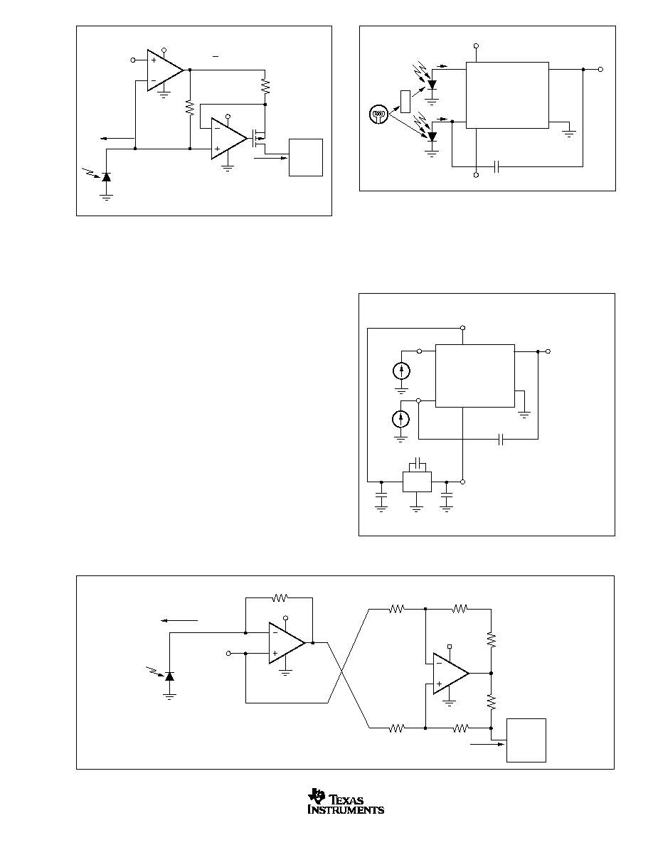
FIGURE 7. Precision Current Inverter/Current Source.
1.5k
Photodiode
10nA to 1mA
10nA to 1mA
+5V
+5V
1.5k
+3.3V
+3.3V
1/2 OPA2335
1/2 OPA2335
OPA2335
1
2
BSH203
TLV271 or
Back Bias
LOG101
Pin 1 or Pin 8
FIGURE 8. Precision Current Inverter/Current Source.
1.5k
+5V
+5V
1.5k
1.5k
100k
10nA to 1mA
LOG101
10nA to 1mA
100k
100k
+3.3V
+3.3V
1/2
OPA2335
1/2
OPA2335
Photodiode
Back Bias
Pin 1 or Pin 8
100k
VOLTAGE INPUTS
The LOG101 gives the best performance with current inputs.
Voltage inputs may be handled directly with series resistors,
but the dynamic input range is limited to approximately three
decades of input voltage by voltage noise and offsets. The
transfer function of Equation (13) applies to this configuration.
APPLICATION CIRCUITS
LOG RATIO
One of the more common uses of log ratio amplifiers is
to measure absorbance. A typical application is shown in
Figure 9.
Absorbance of the sample is A = log
1
¥/
1
(3)
If D
1
and D
2
are matched A
(1V) logI
1
/ I
2
(4)
DATA COMPRESSION
In many applications the compressive effects of the logarith-
mic transfer function are useful. For example, a LOG101
preceding a 12-bit Analog-to-Digital (A/D) converter can
produce the dynamic range equivalent to a 20-bit converter.
FIGURE 9. Absorbance Measurement.
I
2
I
1
8
1
5
6
3
V
OUT
4
V+
V≠
C
C
LOG101
D
2
D
1
Sample
1
1
¥
1
Light
Source
OPERATION ON SINGLE SUPPLY
Many applications do not have the dual supplies required to
operate the LOG101. Figure 10 shows the LOG101 config-
ured for operation with a single +5V supply.
8
1
3
6
4
5
1
2
3
5
4
≠5V
1
µ
F
LOG101
1
µ
F
I
1
I
2
V
OUT
C
C
1
µ
F
TPS
(1)
Single Supply +5V
NOTE: (1) TPS60402DBV negative charge pump.
FIGURE 10. Single +5V Power-Supply Operation.

www.ti.com
LOG101
8
SBOS242B
A
2
A
1
I
1
Q
1
Q
2
V
OUT
= (1V) ∑ LOG
I
1
I
2
I
2
I
1
I
2
+
+
≠
≠
R
2
V
OUT
V
L
R
1
V
BE1
V
BE2
also
V
V
R
R
R
V
R
R
R
n V
I
I
OUT
L
OUT
T
=
+
=
+
1
2
1
1
2
1
1
2
log
V
V
I
I
OUT
=
(
) ∑ log
1
1
2
Using the base-emitter voltage relationship of matched
bipolar transistors, the LOG101 establishes a logarith-
mic function of input current ratios. Beginning with the
base-emitter voltage defined as:
V
V
I
I
where V
kT
q
BE
T
C
S
T
=
=
ln
:
k = Boltzman's constant = 1.381 ∑ 10
≠23
T = Absolute temperature in degrees Kelvin
q = Electron charge = 1.602 ∑ 10
≠19
Coulombs
I
C
= Collector current
I
S
= Reverse saturation current
From the circuit in Figure 11, we see that:
V
V
V
L
BE
BE
=
1
2
≠
Substituting (1) into (2) yields:
V
V
I
I
V
I
I
L
T
S
T
S
=
1
1
1
2
2
2
ln
≠
ln
If the transistors are matched and isothermal and
V
TI
= V
T2
, then (3) becomes:
V
V
I
I
I
I
V
V
I
I
and
ce
x
x
V
n V
I
I
L
T
S
S
L
T
L
T
=
=
=
=
1
1
2
1
2
10
1
2
2 3
ln
≠ ln
ln
sin
ln
. log
log
where n = 2.3
INSIDE THE LOG101
(1)
(2)
(3)
(4)
(5)
(6)
(7)
(9)
(10)
(11)
FIGURE 11. Simplified Model of a Log Amplifier.
(8)
or
It should be noted that the temperature dependance
associated with V
T
= kT/q is internally compensated on
the LOG101 by making R
1
a temperature sensitive resis-
tor with the required positive temperature coefficient.
DEFINITION OF TERMS
TRANSFER FUNCTION
The ideal transfer function is:
V
OUT
= 1V ∑ log (I
1
/I
2
)
Figure 12 shows the graphical representation of the transfer
over valid operating range for the LOG101.
ACCURACY
Accuracy considerations for a log ratio amplifier are some-
what more complicated than for other amplifiers. This is
because the transfer function is nonlinear and has two
inputs, each of which can vary over a wide dynamic range.
The accuracy for any combination of inputs is determined
from the total error specification.
FIGURE 12. Transfer Function with Varying I
2
and I
1
.
(5)
3.0
3.5
2.0
2.5
1.0
1.5
0.5
0.0
≠3.0
≠3.5
≠2.0
≠2.5
≠1.0
≠0.5
≠1.5
1nA
10nA
100nA 1
µ
A
10
µ
A
100
µ
A
1mA
10mA
100pA
V
OUT
(V)
I
2
= 100pA
I
2
= 1nA
I
2
= 1
0n
A
I
2
= 100nA
I
2
= 1
µ
A
I
2
= 10
µ
A
I
2
= 100
µ
A
I
2
= 1mA
I
1
V
OUT
= (1V) ∑ LOG (I
1
/I
2
)

www.ti.com
LOG101
9
SBOS242B
TOTAL ERROR
The total error is the deviation (expressed in mV) of the
actual output from the ideal output of V
OUT
= 1V ∑ log (I
1
/I
2
).
Thus,
V
OUT(ACTUAL)
= V
OUT(IDEAL)
±
Total Error.
It represents the sum of all the individual components of error
normally associated with the log amp when operated in the
current input mode. The worst-case error for any given ratio
of I
1
/I
2
is the largest of the two errors when I
1
and I
2
are
considered separately. Temperature can affect total error.
ERRORS RTO AND RTI
As with any transfer function, errors generated by the func-
tion itself may be Referred-to-Output (RTO) or Referred-to-
Input (RTI). In this respect, log amps have a unique property:
Given some error voltage at the log amp's output, that error
corresponds to a constant percent of the input regardless of
the actual input level.
USING A LARGER REFERENCE VOLTAGE
REDUCES OFFSET ERRORS
Using a larger reference voltage to create the reference
current minimizes errors due to the LOG101's input offset
voltage. Maintaining an increasing output voltage as a func-
tion of increasing photodiode current is also important in
many optical sensing applications. All zeros from the
A/D converter output represent zero or low-scale photodiode
current. Inputting the reference current into I
1
, and designing
I
REF
such that it is as large or larger than the expected
maximum photodiode current is accomplished using this
requirement. The LOG101 configured with the reference
current connecting I
1
and the photodiode current connecting
A
1
A
2
LOG101
Q
1
Q
2
OPA703
R
2
R
3
R
2
6
R
3
C
C
V
OUT
V
REF
I
REF
I
REF
=
I
MIN
to I
MAX
V
REF
R
1
V
OUT
= V
REF
≠ ∑ (1V)LOG
( )
R
2
R
3
I
REF
I
PHOTO
I
1
I
2
8
1
I
PHOTO
A/D
Converter
R
1
V
MIN
to V
MAX
3
FIGURE 13. Technique for Using Full-Scale Reference Current Such that V
OUT
Increases with Increasing Photodiode Current.
to I
2
is shown in Figure 13. The OPA703 is configured as a
level shifter with inverting gain and is used to scale the
photodiode current directly into the A/D converter input
voltage range.
The wide dynamic range of the LOG101 is also useful for
measuring avalanche photodiode current (APD) (see Figure 14).
LOG CONFORMITY
For the LOG101, log conformity is calculated the same as
linearity and is plotted I
1
/I
2
on a semi-log scale. In many
applications, log conformity is the most important specifica-
tion. This is because bias current errors are negligible
(5pA compared to input currents of 100pA and above) and
the scale factor and offset errors may be trimmed to zero or
removed by system calibration. This leaves log conformity as
the major source of error.
Log conformity is defined as the peak deviation from the best
fit straight line of the V
OUT
versus log (I
1
/I
2
) curve. This is
expressed as a percent of ideal full-scale output. Thus, the
nonlinearity error expressed in volts over m decades is:
V
OUT(NONLIN)
= 1V/dec ∑ 2NmV
where N is the log conformity error, in percent.
INDIVIDUAL ERROR COMPONENTS
The ideal transfer function with current input is:
V
V
I
I
OUT
=
( )
∑
1
1
2
log
The actual transfer function with the major components of
error is:
V
V
K
I
I
I
I
Nm
V
OUT
B
B
OS O
=
( )
±
(
)
±
±
1
1
2
1
1
2
2
log
≠
≠
(6)
(7)
(8)
(9)
www.ti.com
LOG101
10
SBOS242B
(10)
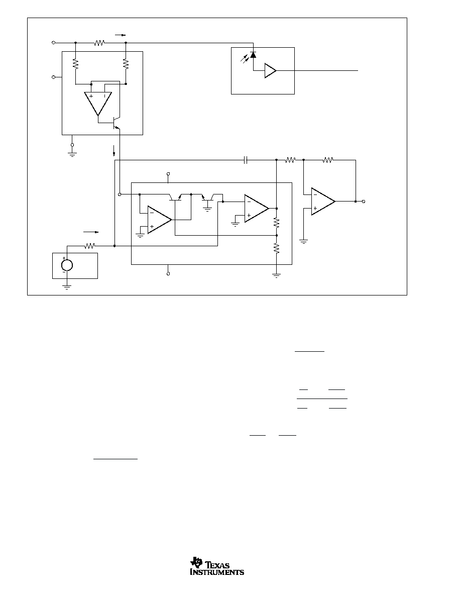
FIGURE 14. High Side Shunt for Avalanche Photodiode (APD) Measures 3-Decades of APD Current.
A
1
≠5V
SO-8
5
LOG101
Q
1
2
Q
2
I
OUT
I
OUT
= 0.1 ∑ I
SHUNT
6
1.2k
Receiver
Irx = 1
µ
A to 1mA
I to V
Converter
APD
10Gbits/sec
1k
C
C
A
2
OPA703
V
OUT
= 2.5V to 0V
I
SHUNT
100
µ
A
500
5k
5k
+15V to +60V
+5V
25k
INA168
SOT23-5
REF3025
2.5V
+5V
1
1
8
4
3
The individual component of error is:
K = gain accuracy (0.15%, typ), as specified in the
specification table.
I
B1
= bias current of A
1
(5pA, typ)
I
B2
= bias current of A
2
(5pA, typ)
N = log conformity error (0.01%, 0.06%, typ)
0.01% for n = 5, 0.06% for n = 7
V
OSO
= output offset voltage (3mV, typ)
n = number of decades over which N is specified:
Example: what is the error when
I
1
= 1
µ
A and I
2
= 100nA
V
mV
OUT
= ±
(
)
-
-
±
( )(
)
±
-
-
-
-
1 0 0015
10
5 10
10
5 10
2 0 0001 5
3 0
6
12
7
12
.
log
∑
∑
.
.
= 1.005055V
(11)
(12)
(13)
Since the ideal output is 1.000V, the error as a percent of
reading is
%
.
%
. %
error
=
∑
=
0 005055
1
100
0 5
For the case of voltage inputs, the actual transfer function is
V
V
K
V
R
I
E
R
V
R
I
E
R
Nn
V
OUT
B
OS
B
OS
OSO
=
( )
±
(
)
±
±
±
±
1
1
2
1
1
1
1
1
2
2
2
2
2
log
≠
≠
Where
E
R
and
E
R
OS
OS
1
1
2
2
are considered to be zero for large
values of resistance from external input current sources.

PACKAGING INFORMATION
Orderable Device
Status
(1)
Package
Type
Package
Drawing
Pins Package
Qty
Eco Plan
(2)
Lead/Ball Finish
MSL Peak Temp
(3)
LOG101AID
ACTIVE
SOIC
D
8
100
None
CU SNPB
Level-3-235C-168 HR
LOG101AIDR
ACTIVE
SOIC
D
8
2500
None
CU SNPB
Level-3-235C-168 HR
(1)
The marketing status values are defined as follows:
ACTIVE: Product device recommended for new designs.
LIFEBUY: TI has announced that the device will be discontinued, and a lifetime-buy period is in effect.
NRND: Not recommended for new designs. Device is in production to support existing customers, but TI does not recommend using this part in
a new design.
PREVIEW: Device has been announced but is not in production. Samples may or may not be available.
OBSOLETE: TI has discontinued the production of the device.
(2)
Eco Plan - May not be currently available - please check
http://www.ti.com/productcontent
for the latest availability information and additional
product content details.
None: Not yet available Lead (Pb-Free).
Pb-Free (RoHS): TI's terms "Lead-Free" or "Pb-Free" mean semiconductor products that are compatible with the current RoHS requirements
for all 6 substances, including the requirement that lead not exceed 0.1% by weight in homogeneous materials. Where designed to be soldered
at high temperatures, TI Pb-Free products are suitable for use in specified lead-free processes.
Green (RoHS & no Sb/Br): TI defines "Green" to mean "Pb-Free" and in addition, uses package materials that do not contain halogens,
including bromine (Br) or antimony (Sb) above 0.1% of total product weight.
(3)
MSL, Peak Temp. -- The Moisture Sensitivity Level rating according to the JEDECindustry standard classifications, and peak solder
temperature.
Important Information and Disclaimer:The information provided on this page represents TI's knowledge and belief as of the date that it is
provided. TI bases its knowledge and belief on information provided by third parties, and makes no representation or warranty as to the
accuracy of such information. Efforts are underway to better integrate information from third parties. TI has taken and continues to take
reasonable steps to provide representative and accurate information but may not have conducted destructive testing or chemical analysis on
incoming materials and chemicals. TI and TI suppliers consider certain information to be proprietary, and thus CAS numbers and other limited
information may not be available for release.
In no event shall TI's liability arising out of such information exceed the total purchase price of the TI part(s) at issue in this document sold by TI
to Customer on an annual basis.
PACKAGE OPTION ADDENDUM
www.ti.com
9-Dec-2004
Addendum-Page 1

IMPORTANT NOTICE
Texas Instruments Incorporated and its subsidiaries (TI) reserve the right to make corrections, modifications,
enhancements, improvements, and other changes to its products and services at any time and to discontinue
any product or service without notice. Customers should obtain the latest relevant information before placing
orders and should verify that such information is current and complete. All products are sold subject to TI's terms
and conditions of sale supplied at the time of order acknowledgment.
TI warrants performance of its hardware products to the specifications applicable at the time of sale in
accordance with TI's standard warranty. Testing and other quality control techniques are used to the extent TI
deems necessary to support this warranty. Except where mandated by government requirements, testing of all
parameters of each product is not necessarily performed.
TI assumes no liability for applications assistance or customer product design. Customers are responsible for
their products and applications using TI components. To minimize the risks associated with customer products
and applications, customers should provide adequate design and operating safeguards.
TI does not warrant or represent that any license, either express or implied, is granted under any TI patent right,
copyright, mask work right, or other TI intellectual property right relating to any combination, machine, or process
in which TI products or services are used. Information published by TI regarding third-party products or services
does not constitute a license from TI to use such products or services or a warranty or endorsement thereof.
Use of such information may require a license from a third party under the patents or other intellectual property
of the third party, or a license from TI under the patents or other intellectual property of TI.
Reproduction of information in TI data books or data sheets is permissible only if reproduction is without
alteration and is accompanied by all associated warranties, conditions, limitations, and notices. Reproduction
of this information with alteration is an unfair and deceptive business practice. TI is not responsible or liable for
such altered documentation.
Resale of TI products or services with statements different from or beyond the parameters stated by TI for that
product or service voids all express and any implied warranties for the associated TI product or service and
is an unfair and deceptive business practice. TI is not responsible or liable for any such statements.
Following are URLs where you can obtain information on other Texas Instruments products and application
solutions:
Products
Applications
Amplifiers
amplifier.ti.com
Audio
www.ti.com/audio
Data Converters
dataconverter.ti.com
Automotive
www.ti.com/automotive
DSP
dsp.ti.com
Broadband
www.ti.com/broadband
Interface
interface.ti.com
Digital Control
www.ti.com/digitalcontrol
Logic
logic.ti.com
Military
www.ti.com/military
Power Mgmt
power.ti.com
Optical Networking
www.ti.com/opticalnetwork
Microcontrollers
microcontroller.ti.com
Security
www.ti.com/security
Telephony
www.ti.com/telephony
Video & Imaging
www.ti.com/video
Wireless
www.ti.com/wireless
Mailing Address:
Texas Instruments
Post Office Box 655303 Dallas, Texas 75265
Copyright
2004, Texas Instruments Incorporated