 | ÐлекÑÑоннÑй компоненÑ: MPY600 | СкаÑаÑÑ:  PDF PDF  ZIP ZIP |
Äîêóìåíòàöèÿ è îïèñàíèÿ www.docs.chipfind.ru
Wide Bandwidth
SIGNAL MULTIPLIER
FEATURES
q
WIDE BANDWIDTH:
75MHz -- Current Output
30MHz -- Voltage Output
q
LOW NOISE
q
LOW FEEDTHROUGH: 60dB (5MHz)
q
GROUND-REFERRED OUTPUT
q
LOW OFFSET VOLTAGE
APPLICATIONS
q
MODULATOR/DEMODULATOR
q
VIDEO SIGNAL PROCESSING
q
CRT GEOMETRY CORRECTION
q
CRT FOCUS CORRECTION
q
VOLTAGE-CONTROLLED CIRCUITS
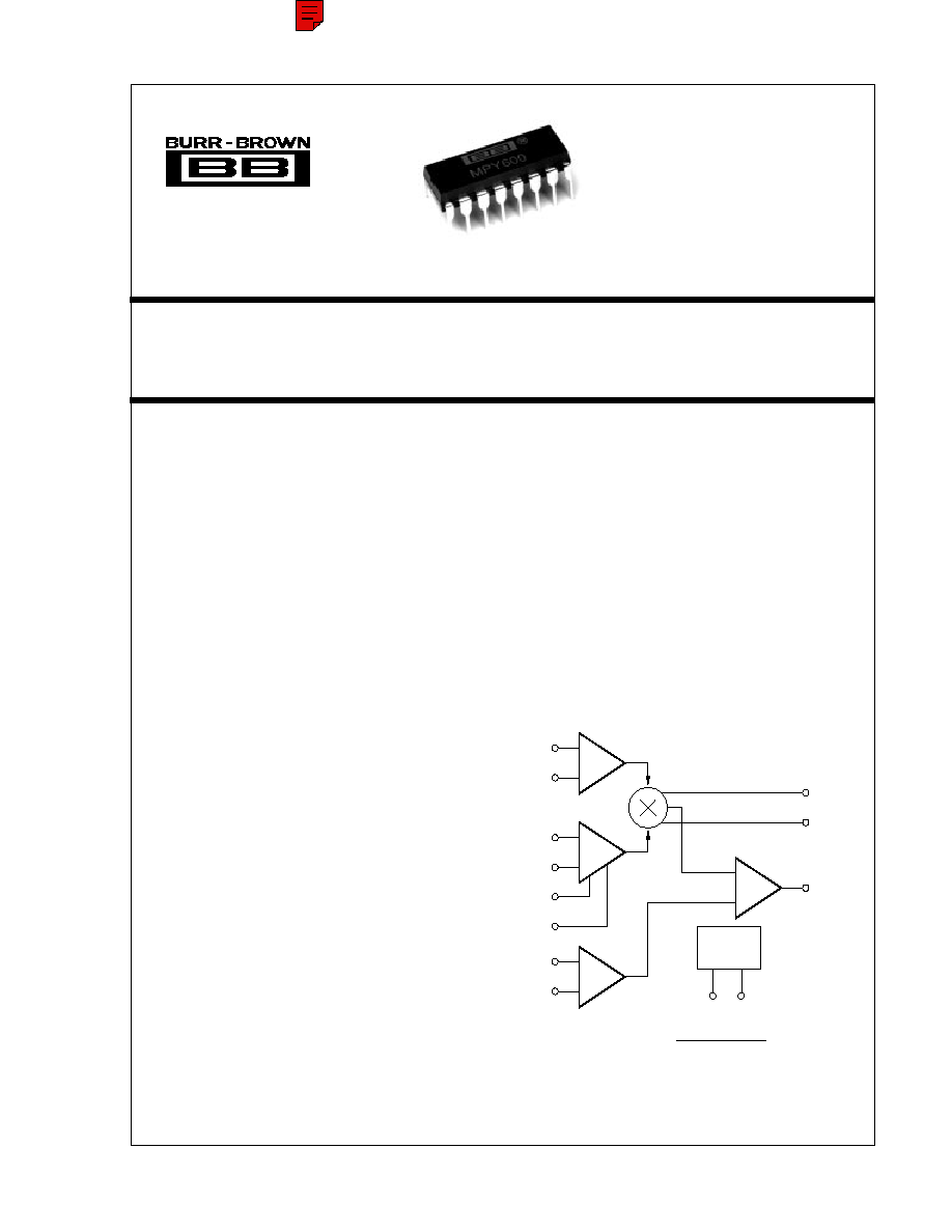
DESCRIPTION
The MPY600 is a wide-bandwidth four-quadrant
signal multiplier. Its output voltage is equal to the
algebraic product of the X and Y input voltages. For
signals up to 30MHz, the on-board output op amp
provides the complete multiplication function with a
low-impedance voltage output. Differential current
outputs extend multiplier bandwidth to 75MHz.
The MPY600 offers improved performance compared
to common semiconductor modulator or multiplier
circuits. It can be used for both two-quadrant (voltage-
controlled amplifier) and four-quadrant (double-
balanced) applications. While previous devices
required cumbersome circuitry for trimming, balance
and level-shifting, the MPY600 requires no external
components. A single external resistor can be used to
program the conversion gain for optimum spurious-
free dynamic range. When used as a modulator, carrier
feedthrough measures 60dB at 5MHz.
Differential X, Y and Z inputs can be connected in a
variety of useful configurations, including squarer,
divider, and square-rooter circuits. The MPY600 is
available in 16-pin plastic DIP, specified for the indus-
trial temperature range.
Multiplier
Core
I = (X X )(Y Y ) mA
X
1
X
2
Y
1
Y
2
R
Y
R
Y
Z
1
Z
2
+
+
+
+
O
1
2
1
2
V
O
I
V Reference
and
Bias
V
S
+V
S
P
I
N
V = A + Z Z
O
2 1
(X X ) (Y Y )
2V
1
2
1
2
[ ]
FPO
MPY600
®
International Airport Industrial Park · Mailing Address: PO Box 11400 · Tucson, AZ 85734 · Street Address: 6730 S. Tucson Blvd. · Tucson, AZ 85706
Tel: (520) 746-1111 · Twx: 910-952-1111 · Cable: BBRCORP · Telex: 066-6491 · FAX: (520) 889-1510 · Immediate Product Info: (800) 548-6132
©
1989 Burr-Brown Corporation
PDS-1019C
Printed in U.S.A. October, 1993

®
MPY600
2
2
SPECIFICATIONS
At V
S
=
±
5V, T
A
=
+25
°
C unless otherwise noted.
MPY600AP
SPECIFICATION
CONDITIONS
MIN
TYP
MAX
UNITS
INPUTS (X, Y, Z)
Full-Scale Differential Input
X
1
-X
2
±
1
V
Y
1
-Y
2
±
2
V
Z
1
-Z
2
±
2
V
Input Voltage Range
±
2.2
V
Differential Input Range
±
2.5
V
Input Impedance
100 || 1.5
k
|| pF
Input Offset Voltage
±
0.5
±
5
mV
Drift
25
µ
V/
°
C
CMRR
V
CM
=
±
2V
70
dB
PSRR
70
dB
Input Bias Current (X, Y)
+15
µ
A
Z Input
15
µ
A
VOLTAGE OUTPUT
(X
1
X
2
)(Y
1
Y
2
)
Transfer Function
V
O
= -------------- + Z
2
V
Total Multiplier Error
(1)
1V
X
1V, 2V
Y
2V
±
15
±
25
mV
2V
X
2V, 2V
Y
2V
±
25
mV
Gain Error
±
1
%
Gain Temperature Drift
±
200
ppm/
°
C
Power Supply Rejection
V
S
=
±
4 to
±
6V
70
dB
Noise
f = 1kHz to 30MHz
120
nV/ Hz
Output Voltage Swing
R
L
= 100
±
2.2
±
3
V
Output Current
±
22
±
30
mA
Short-Circuit Limit
50
mA
Bandwidth
Small Signal
30
MHz
Slew Rate
150
V/
µ
s
Settling Time to 0.1%
4V Step
150
ns
Differential Gain Error
3.58MHz, 0 to 0.7V
0.2
%
Differential Phase Error
3.58MHz, 0 to 0.7V
0.2
Degrees
Capacitive Load, Max
Stable Operation
100
pF
Feedthrough, X
X = 0dBm, f = 500kHz; Y Nulled
65
dB
X = 0dBm, f = 5MHz; Y Nulled
60
dB
Feedthrough, Y
Y = 0dBm, f = 500kHz; X Nulled
70
dB
Y = 0dBm, f = 5MHz; X Nulled
50
dB
Distortion, X
X = 0dBm, f = 500kHz, Y = 2V
60
dB
X = 0dBm, f = 5MHz, Y = 2V
55
dB
Distortion, Y
Y = 0dBm, f = 500kHz, X = 2V
65
dB
Y = 0dBm, f = 5MHz, X = 2V
55
dB
CURRENT OUTPUT
Transfer Function
I
O
= (X
1
X
2
)( Y
1
Y
2
)/1000
A
Total Multiplier Error
(1)
1V
X
1V, 2V
Y
2V
±
20
±
80
µ
A
2V
X
2V, 2V
Y
2V
±
80
µ
A
Gain Error
±
1
%
Gain Temperature Drift
±
200
ppm/
°
C
Power Supply Rejection
V
S
=
±
4 to
±
6V
50
dB
Noise, Output
100
pA/
Hz
Voltage Compliance Range
±
2.5
V
Peak Output Current
5
mA
Noise, Input-Referred
f = 1kHz to 75MHz
50
nV/
Hz
Bandwidth, Small-Signal
75
MHz
Settling Time to 0.1%
4mA Step
150
ns
Feedthrough, X
X = 0dBm, f = 1MHz; Y Nulled
65
dB
X = 0dBm, f = 10MHz; Y Nulled
45
dB
Feedthrough, Y
Y = 0dBm, f = 1MHz; X Nulled
75
dB
Y = 0dBm, f = 10MHz; X Nulled
55
dB
Distortion, X
X = 0dBm, f = 1MHz, Y = 2V
55
dB
X = 0dBm, f = 10MHz, Y = 2V
50
dB
Distortion, Y
Y = 0dBm, f = 1MHz, X = 2V
65
dB
Y = 0dBm, f = 10MHz, X = 2V
50
dB
POWER SUPPLY
Rated Performance
±
5
V
Operating
±
4.75
±
8
V
Current
±
30
±
35
mA
TEMPERATURE RANGE
Specified Temperature Range
25
+85
°
C
Storage Temperature Range
40
+125
°
C
Thermal Resistance,
J-A
50
°
C/W
NOTE: (1) Deviation from ideal transfer function referred to full scale output. Includes gain, nonlinearity and offset errors.
®
MPY600
3
VOLTAGE OUTPUT PHASE SHIFT vs FREQUENCY
1k
10k
100k
1M
10M
100M
100
10
1.0
0.1
0.01
Phase Shift (Deg)
Frequency (Hz)
VOLTAGE OUTPUT FREQUENCY RESPONSE
10k
100k
1M
10M
100M
Frequency (Hz)
30
20
10
0
10
20
V / V (dB)
OUT
Y
R = 0
Y
R = 18
Y
R = 50
Y
R = 100
Y
R = 200
Y
R = 500
Y
R = Open
Y
For X = 1V
20
10
0
10
20
MULTIPLIER GAIN vs FREQUENCY
10k
100k
1M
10M
100M
Frequency (Hz)
Gain (dB)
With 10x Feedback Attenuator
C = 100pF
L
PIN CONFIGURATION
ABSOLUTE MAXIMUM RATINGS
Supply Voltage ...................................................................................
±
18V
Input Voltage Range ............................................................................
±
V
S
Op Amp Output Current ................................................................. 100mA
Operating Temperature ................................................................. +125
°
C
Storage Temperature ..................................................................... +150
°
C
Junction Temperature .................................................................... +150
°
C
Lead Temperature (soldering, 10s) ............................................... +300
°
C
ORDERING INFORMATION
SPECIFIED
TEMPERATURE
MODEL
PACKAGE
RANGE
MPY600AP
16-Pin Plastic DIP
25
°
C to +85
°
C
PACKAGE INFORMATION
PACKAGE DRAWING
MODEL
PACKAGE
NUMBER
(1)
MPY600AP
16-Pin Plastic DIP
180
NOTE: (1) For detailed drawing and dimension table, please see end of data
sheet, or Appendix D of Burr-Brown IC Data Book.
1
2
3
4
5
6
7
8
16
15
14
13
12
11
10
9
V
Z
Z
Y
R
R
Y
+V
I
I
NC
X
NC
NC
X
V
O
1
2
1
Y
Y
2
S
P
N
1
2
S
Voltage Output
Z Input
Z Input
Y Input
Y-Gain Adj.
Y-Gain Adj.
Y Input
+V Power
+Current Output
Current Output
NC
X Input
NC
NC
X Input
V Power
1
2
2
1
S
S
2
1
NC: No internal connection.
Top View
DIP
TYPICAL PERFORMANCE CURVES
T
A
= +25
°
C, V
S
=
±
5V unless otherwise noted.
NOISE FIGURE vs R RESISTANCE
Y
1
10
100
1000
10000
R Resistance ( )
Y
35
30
25
20
15
10
5
Noise Figure (dB)
R = 50
S
®
MPY600
4
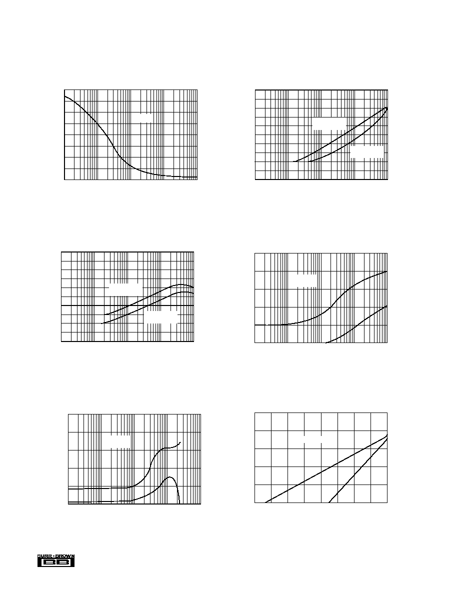
0
20
40
60
80
100
60
40
50
30
20
10
0
10
20
CURRENT OUTPUT HARMONIC DISTORTION
vs INPUT POWER
Input Power (dBm)
Distortion (dBc)
f = 10MHz
2f
3f
VOLTAGE OUTPUT HARMONIC DISTORTION
vs FREQUENCY
30
40
50
60
70
80
10k
100k
1M
10M
100M
Frequency (Hz)
Distortion (dBc)
X = 1V
Y = 0dBm
2f
3f
CURRENT OUTPUT FEEDTHROUGH vs FREQUENCY
1M
10M
100M
100k
10k
0
20
40
60
80
100
Feedthrough (dBc)
Frequency (Hz)
X-Input Nulled
Y-Input 0dBm
Y-Input Nulled
X-Input 0dBm
Y- CHANNEL GAIN vs R RESISTANCE
Y
20
15
10
5
0
1
10
100
1k
10k
R Resistance ( )
Y
Gain: V / V (V/V)
OY
V = 1V
X
TYPICAL PERFORMANCE CURVES
(CONT)
T
A
= +25
°
C, V
S
=
±
5V unless otherwise noted.
CURRENT OUTPUT HARMONIC DISTORTION
vs FREQUENCY
30
40
50
60
70
80
10k
100k
1M
10M
100M
Frequency (Hz)
Distortion (dBc)
X = 1V
Y = 0dBm
2f
3f
VOLTAGE OUTPUT FEEDTHROUGH vs FREQUENCY
1M
10M
100M
100k
10k
0
20
40
60
80
100
Feedthrough (dBc)
Frequency (Hz)
X-Input Nulled
Y-Input 0dBm
Y-Input Nulled
X-Input 0dBm
®
MPY600
5
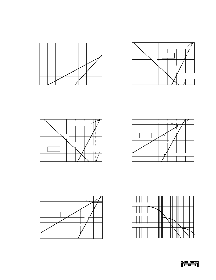
DIVIDER RESPONSE
vs FREQUENCY
60
40
20
0
20
10k
100k
1M
10M
100M
Frequency (Hz)
Gain: V /V
OZ
V = 0.02VDC
Y
V = 0.2VDC
Y
V = 2VDC
Y
OUTPUT-REFERRED DYNAMIC RANGE
vs INPUT POWER
Input Power (dBm)
Output Power (dBm)
40
20
0
20
40
60
80
100
120
100
80
60
40
20
0
20
40
Gain = 0dB
3rd Order IMD
1kHz Noise Floor
1dB Compresion pt
92dB
R =
Y
OUTPUT-REFERRED DYNAMIC RANGE
vs INPUT POWER
Power In (dBm)
Output Power (dBm)
40
20
0
20
40
60
80
100
120
120
100
80
60
40
20
0
20
Gain = 30dB
3rd Order IMD
1kHz Noise Floor
1dB Compresion pt
84dB
R = 0
Y
INPUT-REFERRED DYNAMIC RANGE
vs INPUT POWER
Input Power (dBm)
Dynamic Range (dBc)
0
20
40
60
80
100
140
120
100
80
60
40
20
0
3rd Order IMD
Intercept = 5dBm
1dB Compression
pt = 13dBm
1kHz Noise Floor
R = 0
Y
INPUT-REFERRED DYNAMIC RANGE
vs INPUT POWER
Input Power (dBm)
Dynamic Range (dBc)
0
20
40
60
80
100
100
80
60
40
20
0
20
40
Intercept = 37dBm
1dB Compression
pt = 17dBm
1kHz Noise Floor
3rd Order IMP
3rd Order IMD
R =
Y
0
20
40
60
80
100
60
40
50
30
20
10
0
10
20
VOLTAGE OUTPUT HARMONIC DISTORTION
vs INPUT POWER
Frequency (Hz)
Distortion (dBc)
f = 5MHz
2f
3f
TYPICAL PERFORMANCE CURVES
(CONT)
T
A
= +25
°
C, V
S
=
±
5V unless otherwise noted.