 | –≠–ª–µ–∫—Ç—Ä–æ–Ω–Ω—ã–π –∫–æ–º–ø–æ–Ω–µ–Ω—Ç: OPA132 | –°–∫–∞—á–∞—Ç—å:  PDF PDF  ZIP ZIP |
Document Outline
- FEATURES
- APPLICATIONS
- DESCRIPTION
- OPA380 RELATED DEVICES
- ABSOLUTE MAXIMUM RATINGS(1)
- PACKAGE/ORDERING INFORMATION(1)
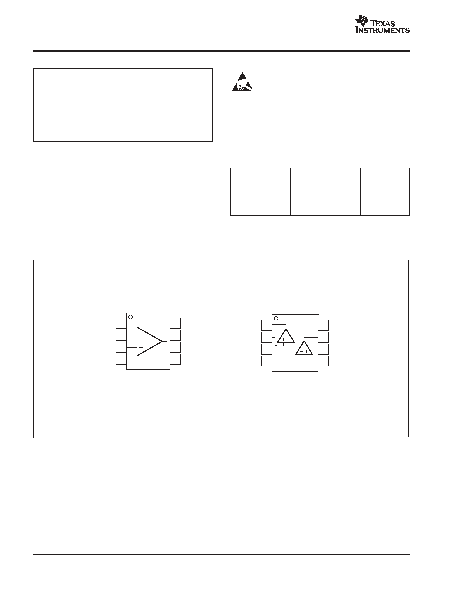
- PIN ASSIGNMENTS
- ELECTRICAL CHARACTERISTICS: OPA380 (SINGLE), VS = 2.7V to 5.5V
- ELECTRICAL CHARACTERISTICS: OPA2380 (DUAL), VS = 2.7V to 5.5V
- TYPICAL CHARACTERISTICS: VS = + 2.7V to + 5.5V
- APPLICATIONS INFORMATION
- BASIC OPERATION
- OPERATING VOLTAGE
- INTERNAL OFFSET CORRECTION
- INPUT VOLTAGE
- INPUT OVERVOLTAGE PROTECTION
- OUTPUT RANGE
- OVERLOAD RECOVERY
- ACHIEVING OUTPUT SWING TO GROUND
- BIASING PHOTODIODES IN SINGLE-SUPPLY CIRCUITS
- TRANSIMPEDANCE AMPLIFIER
- TRANSIMPEDANCE BANDWIDTH AND NOISE
- BOARD LAYOUT
- OTHER WAYS TO MEASURE SMALL CURRENTS
- CAPACITIVE LOAD AND STABILITY
- DRIVING FAST 16-BIT ANALOG-TO-DIGITAL CONVERTERS ( ADC)

FEATURES
D
> 1MHz TRANSIMPEDANCE BANDWIDTH
D
EXCELLENT LONG-TERM V
OS
STABILITY
D
BIAS CURRENT: 50pA (max)
D
OFFSET VOLTAGE: 25
µ
V (max)
D
INPUT CURRENT RANGE: 10nA to 1mA
D
DRIFT: 0.1
µ
V/
∞
C (max)
D
GAIN BANDWIDTH: 90MHz
D
QUIESCENT CURRENT: 6.5mA
D
SUPPLY RANGE: 2.7V to 5.5V
D
SINGLE AND DUAL VERSIONS
D
MicroSize PACKAGE: MSOP-8
APPLICATIONS
D
PHOTODIODE MONITORING
D
PRECISION I/V CONVERSION
D
OPTICAL AMPLIFIERS
D
CAT-SCANNER FRONT-END
1M
R
F
100k
+5V
7
2
3
4
6
OPA380
67pF
75pF
-
5V
R
P
(Optional
Pulldown
Resistor)
V
OUT
(0V to 4.4V)
Photodiode
DESCRIPTION
The OPA380 family of transimpedance amplifiers provides
high-speed (90MHz Gain Bandwidth [GBW]) operation, with
extremely high precision, excellent long-term stability, and
very low 1/f noise. It is ideally suited for high-speed
photodiode applications. The OPA380 features an offset
voltage of 25
µ
V, offset drift of 0.1
µ
V/
∞
C, and bias current of
50pA. The OPA380 far exceeds the offset, drift, and noise
performance that conventional JFET op amps provide.
The signal bandwidth of a transimpedance amplifier depends
largely on the GBW of the amplifier and the parasitic
capacitance of the photodiode, as well as the feedback
resistor. The 90MHz GBW of the OPA380 enables a trans-
impedance bandwidth of > 1MHz in most configurations. The
OPA380 is ideally suited for fast control loops for power level
on an optical fiber.
As a result of the high precision and low-noise characteristics
of the OPA380, a dynamic range of 5 decades can be
achieved. This capability allows the measurement of signal
currents in the order of 10nA, and up to 1mA in a single I/V
conversion stage. In contrast to logarithmic amplifiers, the
OPA380 provides very wide bandwidth throughout the full
dynamic range. By using an external pulldown resistor to
≠5V, the output voltage range can be extended to include 0V.
The OPA380 (single) is available in MSOP-8 and SO-8
packages. The OPA2380 (dual) is available in the
miniature MSOP-8 package. They are specified from
≠40
∞
C to +125
∞
C.
OPA380 RELATED DEVICES
PRODUCT
FEATURES
OPA300
150MHz CMOS, 2.7V to 5.5V Supply
OPA350
500
µ
V VOS, 38MHz, 2.5V to 5V Supply
OPA335
10
µ
V VOS, Zero-Drift, 2.5V to 5V Supply
OPA132
16MHz GBW, Precision FET Op Amp,
±
15V
OPA656/7
230MHz, Precision FET,
±
5V
LOG112
LOG amp, 7.5 decades,
±
4.5V to
±
18V Supply
LOG114
LOG amp, 7.5 decades,
±
2.25V to
±
5.5V Supply
IVC102
Precision Switched Integrator
DDC112
Dual Current Input, 20-Bit ADC
OPA380
OPA2380
SBOS291E - NOVEMBER 2003 - REVISED NOVEMBER 2004
Precision, High-Speed
Transimpedance Amplifier
PRODUCTION DATA information is current as of publication date. Products
conform to specifications per the terms of Texas Instruments standard warranty.
Production processing does not necessarily include testing of all parameters.
www.ti.com
Copyright
2003-2004, Texas Instruments Incorporated
All trademarks are the property of their respective owners.
Please be aware that an important notice concerning availability, standard warranty, and use in critical applications of Texas Instruments
semiconductor products and disclaimers thereto appears at the end of this data sheet.
OPA380
OPA2380
SBOS291E - NOVEMBER 2003 - REVISED NOVEMBER 2004
www.ti.com
2
ABSOLUTE MAXIMUM RATINGS
(1)
Voltage Supply
+7V
. . . . . . . . . . . . . . . . . . . . . . . . . . . . . . . . . . . . . . .
Signal Input Terminals(2), Voltage
-0.5V to (V+) + 0.5V
. . . . . . . . . .
Current
±
10mA
. . . . . . . . . . . . . . . . . . . . .
Short-Circuit Current(3)
Continuous
. . . . . . . . . . . . . . . . . . . . . . . .
Operating Temperature Range
-40
∞
C to +125
∞
C
. . . . . . . . . . . . . . .
Storage Temperature Range
-65
∞
C to +150
∞
C
. . . . . . . . . . . . . . . . .
Junction Temperature
+150
∞
C
. . . . . . . . . . . . . . . . . . . . . . . . . . . . . . .
Lead Temperature (soldering, 10s)
+300
∞
C
. . . . . . . . . . . . . . . . . . . . .
ESD Rating (Human Body Model)
2000V
. . . . . . . . . . . . . . . . . . . . . . .
(1) Stresses above these ratings may cause permanent damage.
Exposure to absolute maximum conditions for extended periods
may degrade device reliability. These are stress ratings only, and
functional operation of the device at these or any other conditions
beyond those specified is not implied.
(2) Input terminals are diode clamped to the power-supply rails. Input
signals that can swing more than 0.5V beyond the supply rails
should be current limited to 10mA or less.
(3) Short-circuit to ground; one amplifier per package.
ELECTROSTATIC DISCHARGE SENSITIVITY
This integrated circuit can be damaged by ESD. Texas
Instruments recommends that all integrated circuits be
handled with appropriate precautions. Failure to observe
proper handling and installation procedures can cause damage.
ESD damage can range from subtle performance degradation to
complete device failure. Precision integrated circuits may be more
susceptible to damage because very small parametric changes could
cause the device not to meet its published specifications.
PACKAGE/ORDERING INFORMATION
(1)
PRODUCT
PACKAGE-LEAD
PACKAGE
MARKING
OPA380
MSOP-8
AUN
OPA380
MSOP-8
AUN
OPA380
SO-8
OPA380A
OPA380
SO-8
OPA380A
OPA2380
MSOP-8
BBX
OPA2380
MSOP-8
BBX
(1) For the most current package and ordering information, see the
Package Option Addendum located at the end of this data sheet.
PIN ASSIGNMENTS
Top View
1
2
3
4
8
7
6
5
NC
(1)
V+
Out
NC
(1)
NC
(1)
-
In
+In
V
-
OPA380
MSOP-8, SO-8
NOTES: (1) NC indicates no internal connection.
1
2
3
4
8
7
6
5
V+
Out B
-
In B
+In B
Out A
-
In A
+In A
V
-
OPA2380
MSOP-8

OPA380
OPA2380
SBOS291E - NOVEMBER 2003 - REVISED NOVEMBER 2004
www.ti.com
3
ELECTRICAL CHARACTERISTICS: OPA380 (SINGLE), V
S
= 2.7V to 5.5V
Boldface limits apply over the temperature range, T
A
= -40
∞
C to +125
∞
C.
All specifications at TA = +25
∞
C, RL = 2k
connected to VS/2, and VOUT = VS/2, unless otherwise noted.
OPA380
PARAMETER
CONDITION
MIN
TYP
MAX
UNITS
OFFSET VOLTAGE
Input Offset Voltage
VOS
VS = +5V, VCM = 0V
4
25
µ
V
Drift
dVOS/dT
0.03
0.1
µ
V/
∞
C
vs Power Supply
PSRR
VS = +2.7V to +5.5V, VCM = 0V
2.4
10
µ
V/V
Over Temperature
VS = +2.7V to +5.5V, VCM = 0V
10
µ
V/V
Long-Term Stability(1)
See Note (1)
Channel Separation, dc
1
µ
V/V
INPUT BIAS CURRENT
Input Bias Current
IB
VCM = VS/2
3
±
50
pA
Over Temperature
Typical Characteristics
Input Offset Current
IOS
VCM = VS/2
6
±
100
pA
NOISE
Input Voltage Noise, f = 0.1Hz to 10Hz
en
VS = +5V, VCM = 0V
3
µ
V
PP
Input Voltage Noise Density, f = 10kHz
en
VS = +5V, VCM = 0V
67
nV/
Hz
Input Voltage Noise Density, f > 1MHz
en
VS = +5V, VCM = 0V
5.8
nV/
Hz
Input Current Noise Density, f = 10kHz
in
VS = +5V, VCM = 0V
10
fA/
Hz
INPUT VOLTAGE RANGE
Common-Mode Voltage Range
VCM
V-
(V+) - 1.8V
V
Common-Mode Rejection Ratio
CMRR
(V-) < VCM < (V+) ≠ 1.8V
100
110
dB
INPUT IMPEDANCE
Differential Capacitance
1.1
pF
Common-Mode Resistance and Inverting Input
Capacitance
1013 || 3
|| pF
OPEN-LOOP GAIN
Open-Loop Voltage Gain
AOL
0.1V < VO < (V+) - 0.7V, VS = 5V, VCM = VS/2
110
130
dB
0.1V < VO < (V+) - 0.6V, VS = 5V, VCM = VS/2,
TA = -40
∞
C to +85
∞
C
110
130
dB
0V < VO < (V+) - 0.7V, VS = 5V, VCM = 0V,
RP = 2k
to -5V(2)
106
120
dB
0V < VO < (V+) - 0.6V, VS = 5V, VCM = 0V,
RP = 2k
to -5V(2), TA = -40
∞
C to +85
∞
C
106
120
dB
FREQUENCY RESPONSE
CL = 50pF
Gain-Bandwidth Product
GBW
90
MHz
Slew Rate
SR
G = +1
80
V/
µ
s
Settling Time, 0.01%(3)
tS
VS = +5V, 4V Step, G = +1
2
µ
s
Overload Recovery Time(4)(5)
VIN
∑
G = > VS
100
ns
OUTPUT
Voltage Output Swing from Positive Rail
RL = 2k
400
600
mV
Voltage Output Swing from Negative Rail
RL = 2k
60
100
mV
Voltage Output Swing from Positive Rail
RP = 2k
to -5V(2)
400
600
mV
Voltage Output Swing from Negative Rail
RP = 2k
to -5V(2)
-20
0
mV
Output Current
IOUT
See Typical Characteristics
Short-Circuit Current
ISC
150
mA
Capacitive Load Drive
CLOAD
See Typical Characteristics
Open-Loop Output Impedance
RO
f = 1MHz, IO = 0A
40
POWER SUPPLY
Specified Voltage Range
VS
2.7
5.5
V
Quiescent Current
IQ
IO = 0A
6.5
8.3
mA
Over Temperature
8.8
mA
TEMPERATURE RANGE
Specified and Operating Range
-40
+125
∞
C
Storage Range
-65
+150
∞
C
Thermal Resistance
q
JA
MSOP-8, SO-8
150
∞
C/W
(1) 300-hour life test at 150
∞
C demonstrated randomly distributed variation approximately equal to measurement repeatability of 1
µ
V.
(2) Tested with output connected only to RP, a pulldown resistor connected between VOUT and -5V, as shown in Figure 5. See also applications section, Achieving
Output Swing to Ground.
(3) Transimpedance frequency of 1MHz.
(4) Time required to return to linear operation.
(5) From positive rail.

OPA380
OPA2380
SBOS291E - NOVEMBER 2003 - REVISED NOVEMBER 2004
www.ti.com
4
ELECTRICAL CHARACTERISTICS: OPA2380 (DUAL), V
S
= 2.7V to 5.5V
Boldface limits apply over the temperature range, T
A
= -40
∞
C to +125
∞
C.
All specifications at TA = +25
∞
C, RL = 2k
connected to VS/2, and VOUT = VS/2, unless otherwise noted.
OPA2380
PARAMETER
CONDITION
MIN
TYP
MAX
UNITS
OFFSET VOLTAGE
Input Offset Voltage
VOS
VS = +5V, VCM = 0V
4
25
µ
V
Drift
dVOS/dT
0.03
0.1
µ
V/
∞
C
vs Power Supply
PSRR
VS = +2.7V to +5.5V, VCM = 0V
2.4
10
µ
V/V
Over Temperature
VS = +2.7V to +5.5V, VCM = 0V
10
µ
V/V
Long-Term Stability(1)
See Note (1)
Channel Separation, dc
1
µ
V/V
INPUT BIAS CURRENT
Input Bias Current, Inverting Input
IB
VCM = VS/2
3
±
50
pA
Noninverting Input
IB
VCM = VS/2
3
±
200
pA
Over Temperature
Typical Characteristics
NOISE
Input Voltage Noise, f = 0.1Hz to 10Hz
en
VS = +5V, VCM = 0V
3
µ
V
PP
Input Voltage Noise Density, f = 10kHz
en
VS = +5V, VCM = 0V
67
nV/
Hz
Input Voltage Noise Density, f > 1MHz
en
VS = +5V, VCM = 0V
5.8
nV/
Hz
Input Current Noise Density, f = 10kHz
in
VS = +5V, VCM = 0V
10
fA/
Hz
INPUT VOLTAGE RANGE
Common-Mode Voltage Range
VCM
V-
(V+) - 1.8V
V
Common-Mode Rejection Ratio
CMRR
(V-) < VCM < (V+) ≠ 1.8V
95
105
dB
INPUT IMPEDANCE
Differential Capacitance
1.1
pF
Common-Mode Resistance and Inverting Input
Capacitance
1013 || 3
|| pF
OPEN-LOOP GAIN
Open-Loop Voltage Gain
AOL
0.12V < VO < (V+) - 0.7V, VS = 5V, VCM = VS/2
110
130
dB
0.12V < VO < (V+) - 0.6V, VS = 5V, VCM = VS/2,
TA = -40
∞
C to +85
∞
C
110
130
dB
0V < VO < (V+) - 0.7V, VS = 5V, VCM = 0V,
RP = 2k
to -5V(2)
106
120
dB
0V < VO < (V+) - 0.6V, VS = 5V, VCM = 0V,
RP = 2k
to -5V(2), TA = -40
∞
C to +85
∞
C
106
120
dB
FREQUENCY RESPONSE
CL = 50pF
Gain-Bandwidth Product
GBW
90
MHz
Slew Rate
SR
G = +1
80
V/
µ
s
Settling Time, 0.01%(3)
tS
VS = +5V, 4V Step, G = +1
2
µ
s
Overload Recovery Time(4), (5)
VIN
∑
G = > VS
100
ns
OUTPUT
Voltage Output Swing from Positive Rail
RL = 2k
400
600
mV
Voltage Output Swing from Negative Rail
RL = 2k
80
120
mV
Voltage Output Swing from Positive Rail
RP = 2k
to -5V(2)
400
600
mV
Voltage Output Swing from Negative Rail
RP = 2k
to -5V(2)
-20
0
mV
Output Current
IOUT
See Typical Characteristics
Short-Circuit Current
ISC
150
mA
Capacitive Load Drive
CLOAD
See Typical Characteristics
Open-Loop Output Impedance
RO
f = 1MHz, IO = 0A
40
POWER SUPPLY
Specified Voltage Range
VS
2.7
5.5
V
Quiescent Current (per amplifier)
IQ
IO = 0A
7.5
9.5
mA
Over Temperature
10
mA
TEMPERATURE RANGE
Specified and Operating Range
-40
+125
∞
C
Storage Range
-65
+150
∞
C
Thermal Resistance
q
JA
MSOP-8
150
∞
C/W
(1) 300-hour life test at 150
∞
C demonstrated randomly distributed variation approximately equal to measurement repeatability of 1
µ
V.
(2) Tested with output connected only to RP, a pulldown resistor connected between VOUT and -5V, as shown in Figure 5. See also applications section, Achieving
Output Swing to Ground.
(3) Transimpedance frequency of 1MHz.
(4) Time required to return to linear operation.
(5) From positive rail.

OPA380
OPA2380
SBOS291E - NOVEMBER 2003 - REVISED NOVEMBER 2004
www.ti.com
5
TYPICAL CHARACTERISTICS: V
S
= +2.7V to +5.5V
All specifications at TA = +25
∞
C, RL = 2k
connected to VS/2, and VOUT = VS/2, unless otherwise noted.
140
120
100
80
60
40
20
0
-
20
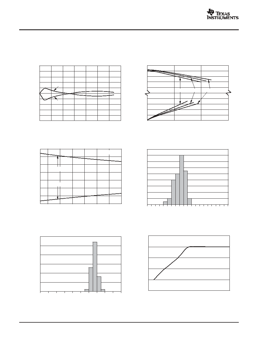
OPEN-LOOP GAIN AND PHASE vs FREQUENCY
Frequency (Hz)
O
p
e
n
-
L
oo
p
G
ai
n
(
d
B
)
90
45
0
-
45
-
90
-
135
-
180
-
225
-
270
P
has
e
(
_
)
10
100
10M
1M
10k
100k
1k
100M
Gain
Phase
160
140
120
100
80
60
40
20
0
-
20
POWER-SUPPLY REJECTION RATIO AND
COMMON-MODE REJECTION vs FREQUENCY
Frequency (Hz)
P
S
R
R,
CM
RR
(
d
B
)
0.1
1
100k
10M
1M
1k
10k
10
100
100M
PSRR
CMRR
1000
100
10
1
INPUT VOLTAGE NOISE SPECTRAL DENSITY
Frequency (Hz)
I
n
p
u
t
V
ol
ta
ge
N
o
i
s
e
(
nV
/
(H
z
)
10
100
100k
1M
10k
1k
10M
8
7
6
5
4
3
2
1
0
QUIESCENT CURRENT vs TEMPERATURE
Temperature (
_
C)
Q
u
i
e
s
c
ent
C
u
r
r
e
n
t
(
mA
)
-
40
-
25
0
25
50
75
100
125
V
S
= +2.7V
V
S
= +5.5V
7
6
5
4
3
2
1
0
QUIESCENT CURRENT vs SUPPLY VOLTAGE
Supply Voltage (V)
Q
u
i
e
s
c
en
t
C
ur
r
e
n
t
(
m
A
)
2.7
3.0
3.5
4.0
4.5
5.0
5.5
1000
100
10
1
INPUT BIAS CURRENT vs TEMPERATURE
Temperature (
_
C)
I
n
p
u
t
B
i
as
C
u
r
r
en
t
(
p
A
)
-
40
100
125
-
25
0
25
50
75
OPA380
OPA2380
SBOS291E - NOVEMBER 2003 - REVISED NOVEMBER 2004
www.ti.com
6
TYPICAL CHARACTERISTICS: V
S
= +2.7V to +5.5V (continued)
All specifications at TA = +25
∞
C, RL = 2k
connected to VS/2, and VOUT = VS/2, unless otherwise noted.
25
20
15
10
5
0
-
5
-
10
-
15
-
20
-
25
INPUT BIAS CURRENT
vs INPUT COMMON-MODE VOLTAGE
Input Common-Mode Voltage (V)
-
I
B
+
I
B
Input
B
i
a
s
C
u
r
r
ent
(
p
A
)
0
0.5
1.0
1.5
2.0
2.5
3.0
3.5
OUTPUT VOLTAGE SWING vs OUTPUT CURRENT
+125
_
C
+25
_
C
-
40
_
C
Ou
t
p
u
t
S
w
i
n
g
(
V
)
50
100
150
0
(V+)
(V+)
-
1
(V+)
-
2
(V
-
) +2
(V
-
) +1
(V
-
)
Output Current (mA)
-
40
100
125
-
25
0
25
50
75
SHORT-CIRCUIT CURRENT vs TEMPERATURE
S
h
o
r
t-
C
i
r
c
ui
t
C
ur
r
e
nt
(
m
A
)
200
150
100
50
0
-
50
-
100
-
150
Temperature (
_
C)
V
S
= 5V
+I
SC
-
I
SC
OFFSET VOLTAGE PRODUCTION DISTRIBUTION
Offset Voltage (
µ
V)
-
25
-
20
-
15
-
10
-
5
0
5
10
15
20
25
Po
p
u
la
t
i
o
n
OFFSET VOLTAGE DRIFT
PRODUCTION DISTRIBUTION
Offset Voltage Drift (
µ
V/
_
C)
-
0.10
-
0.08
-
0.06
-
0.04
-
0.02
0
0.02
0.04
0.06
0.08
0.1
Po
p
u
la
t
i
o
n
GAIN BANDWIDTH vs POWER SUPPLY VOLTAGE
G
a
i
n
B
and
w
i
dt
h
(
M
H
z
)
3.5
4.5
5.5
2.5
95
90
85
80
75
70
Power Supply Voltage (V)

OPA380
OPA2380
SBOS291E - NOVEMBER 2003 - REVISED NOVEMBER 2004
www.ti.com
7
TYPICAL CHARACTERISTICS: V
S
= +2.7V to +5.5V (continued)
All specifications at TA = +25
∞
C, RL = 2k
connected to VS/2, and VOUT = VS/2, unless otherwise noted.
C
F
Circuit for Transimpedance Amplifier Characteristic curves on this page.
R
F
C
DIODE
OPA380
C
STRAY
TRANSIMPEDANCE AMP CHARACTERISTIC
100
140
130
120
110
100
90
80
70
60
50
40
30
20
1k
10k
100k
1M
10M
100M
Frequency (Hz)
T
r
a
n
s
i
mp
eda
n
c
e
G
ai
n
(
V
/
A
i
n
d
B
)
R
F
= 10M
C
STRAY
(parasitic) = 0.2pF
C
DIODE
= 100pF
R
F
= 1M
C
F
= 0.5pF
R
F
= 100k
R
F
= 10k
R
F
= 1k
C
F
= 2pF
C
F
= 5pF
C
F
= 18pF
TRANSIMPEDANCE AMP CHARACTERISTIC
100
140
130
120
110
100
90
80
70
60
50
40
30
20
1k
10k
100k
1M
10M
100M
Frequency (Hz)
T
r
a
n
s
i
mp
eda
n
c
e
G
ai
n
(
V
/
A
i
n
d
B
)
R
F
= 10M
R
F
= 1M
C
F
= 0.5pF
R
F
= 100k
R
F
= 10k
R
F
= 1k
C
F
= 1.5pF
C
F
= 4pF
C
F
= 12pF
C
STRAY
(parasitic) = 0.2pF
C
DIODE
= 50pF
TRANSIMPEDANCE AMP CHARACTERISTIC
100
140
130
120
110
100
90
80
70
60
50
40
30
1k
10k
100k
1M
10M
100M
Frequency (Hz)
T
r
a
n
s
i
mp
eda
n
c
e
G
ai
n
(
V
/
A
i
n
d
B
)
R
F
= 10M
R
F
= 1M
R
F
= 100k
R
F
= 10k
R
F
= 1k
C
F
= 1pF
C
F
= 2.5pF
C
F
= 7pF
C
STRAY
(parasitic) = 0.2pF
C
DIODE
= 20pF
TRANSIMPEDANCE AMP CHARACTERISTIC
100
140
130
120
110
100
90
80
70
60
50
40
30
1k
10k
100k
1M
10M
100M
Frequency (Hz)
T
r
a
n
s
i
mp
eda
n
c
e
G
ai
n
(
V
/
A
i
n
d
B
)
R
F
= 10M
R
F
= 1M
R
F
= 100k
R
F
= 10k
R
F
= 1k
C
F
= 0.5pF
C
F
= 2pF
C
F
= 5pF
C
STRAY
(parasitic) = 0.2pF
C
DIODE
= 10pF
TRANSIMPEDANCE AMP CHARACTERISTIC
100
140
130
120
110
100
90
80
70
60
50
40
1k
10k
100k
1M
10M
100M
Frequency (Hz)
T
r
a
n
s
i
mp
eda
n
c
e
G
ai
n
(
V
/
A
i
n
d
B
)
R
F
= 10M
R
F
= 1M
R
F
= 100k
R
F
= 10k
R
F
= 1k
C
F
= 0.5pF
C
F
= 1pF
C
F
= 2.5pF
C
STRAY
(parasitic) = 0.2pF
C
DIODE
= 1pF

OPA380
OPA2380
SBOS291E - NOVEMBER 2003 - REVISED NOVEMBER 2004
www.ti.com
8
TYPICAL CHARACTERISTICS: V
S
= +2.7V to +5.5V (continued)
All specifications at TA = +25
∞
C, RL = 2k
connected to VS/2, and VOUT = VS/2, unless otherwise noted.
SMALL-SIGNAL OVERSHOOT vs LOAD CAPACITANCE
O
v
er
s
hoo
t
(
%
)
100
1000
10
50
45
40
35
30
25
20
15
10
5
0
Load Capacitance (pF)
R
S
= 100
No R
S
-
5 V
V
OUT
R
P
= 2 k
C
R
S
+5V
O PA 38 0
2.5pF
10k
SMALL-SIGNAL OVERSHOOT vs LOAD CAPACITANCE
Ove
r
sh
o
o
t
(
%
)
100
1000
10
50
45
40
35
30
25
20
15
10
5
0
Load Capacitance (pF)
R
S
= 100
No R
S
V
O U T
R
F
= 2k
C
R
S
+2.5V
-
2.5V
OPA380
2.5pF
10k
OVERLOAD RECOVERY
0
0
0
.8
m
A
/
d
i
v
2
V
/d
i
v
Time (100ns/div)
3. 2pF
V P
V OUT
2 k
5 0k
+ 5 V
IIN
1.6 m A
V
P
= 0V
V
P
=
-
5V
V
OUT
I
IN
SMALL-SIGNAL STEP RESPONSE
50
mV
/di
v
Time (100ns/div)
R
L
= 2k
LARGE-SIGNAL STEP RESPONSE
1V
/di
v
Time (100ns/div)
R
L
= 2k
10k
2.5V
-
2.5V
2k
2.5pF
CHANNEL SEPARATION vs INPUT FREQUENCY
10
140
120
100
80
60
40
20
0
100
1k
10k
100k
1M
10M
100M
Frequency (Hz)
C
han
nel
S
e
p
a
r
a
ti
o
n
(
d
B
)

OPA380
OPA2380
SBOS291E - NOVEMBER 2003 - REVISED NOVEMBER 2004
www.ti.com
9
APPLICATIONS INFORMATION
BASIC OPERATION
The OPA380 is a high-performance transimpedance
amplifier with very low 1/f noise. As a result of its unique
architecture, the OPA380 has excellent long-term input
voltage offset stability--a 300-hour life test at 150
∞
C
demonstrated randomly distributed variation
approximately equal to measurement repeatability of
1
µ
V.
The OPA380 performance results from an internal
auto-zero amplifier combined with a high-speed
amplifier. The OPA380 has been designed with circuitry
to improve overload recovery and settling time over a
traditional composite approach. It has been specifically
designed and characterized to accommodate circuit
options to allow 0V output operation (see Figure 3).
The OPA380 is used in inverting configurations, with the
noninverting input used as a fixed biasing point.
Figure 1 shows the OPA380 in a typical configuration.
Power-supply pins should be bypassed with 1
µ
F ceramic
or tantalum capacitors. Electrolytic capacitors are not
recommended.
OPA380
V
OUT
(1)
(0.5V to 4.4V)
V
BIAS
= 0.5V
+5V
1
µ
F
R
F
C
F
NOTE: (1) V
OUT
= 0.5V in dark conditions.
Figure 1. OPA380 typical configuration
OPERATING VOLTAGE
OPA380 series op amps are fully specified from 2.7V to
5.5V over a temperature range of -40
∞
C to +125
∞
C.
Parameters that vary significantly with operating
voltages or temperature are shown in the Typical
Characteristics.
INTERNAL OFFSET CORRECTION
The OPA380 series op amps use an auto-zero topology
with a time-continuous 90MHz op amp in the signal
path. This amplifier is zero-corrected every 100
µ
s using
a proprietary technique. Upon power-up, the amplifier
requires approximately 400
µ
s to achieve specified V
OS
accuracy, which includes one full auto-zero cycle of
approximately 100
µ
s and the start-up time for the bias
circuitry. Prior to this time, the amplifier will function
properly but with unspecified offset voltage.
This design has virtually no aliasing and very low noise.
Zero correction occurs at a 10kHz rate, but there is very
little fundamental noise energy present at that
frequency due to internal filtering. For all practical
purposes, any glitches have energy at 20MHz or higher
and are easily filtered, if required. Most applications are
not sensitive to such high-frequency noise, and no
filtering is required.
INPUT VOLTAGE
The input common-mode voltage range of the OPA380
series extends from V- to (V+) ≠1.8V. With input signals
above this common-mode range, the amplifier will no
longer provide a valid output value, but it will not latch
or invert.
INPUT OVERVOLTAGE PROTECTION
Device inputs are protected by ESD diodes that will
conduct if the input voltages exceed the power supplies
by more than approximately 500mV. Momentary
voltages greater than 500mV beyond the power supply
can be tolerated if the current is limited to 10mA. The
OPA380 series feature no phase inversion when the
inputs extend beyond supplies if the input is current
limited.
OPA380
OPA2380
SBOS291E - NOVEMBER 2003 - REVISED NOVEMBER 2004
www.ti.com
10
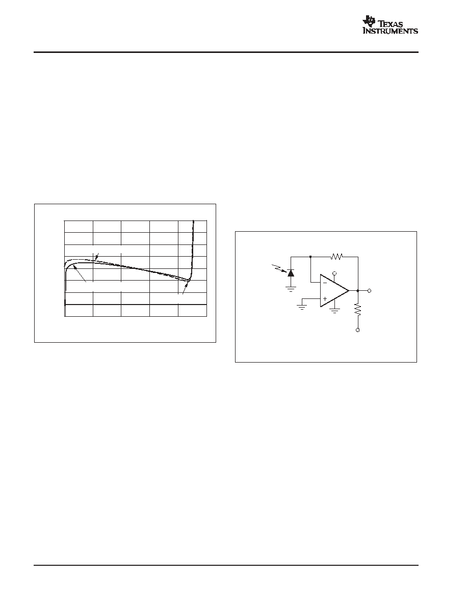
OUTPUT RANGE
The OPA380 is specified to swing within at least 600mV
of the positive rail and 100mV of the negative rail with
a 2k
load with excellent linearity. Swing to the negative
rail while maintaining good linearity can be extended to
0V--see the section, Achieving Output Swing to
Ground. See the Typical Characteristic curve, Output
Voltage Swing vs Output Current.
The OPA380 can swing slightly closer than specified to
the positive rail; however, linearity will decrease and a
high-speed overload recovery clamp limits the amount
of positive output voltage swing available--see
Figure 2.
20
15
10
5
0
-
5
-
10
-
15
-
20
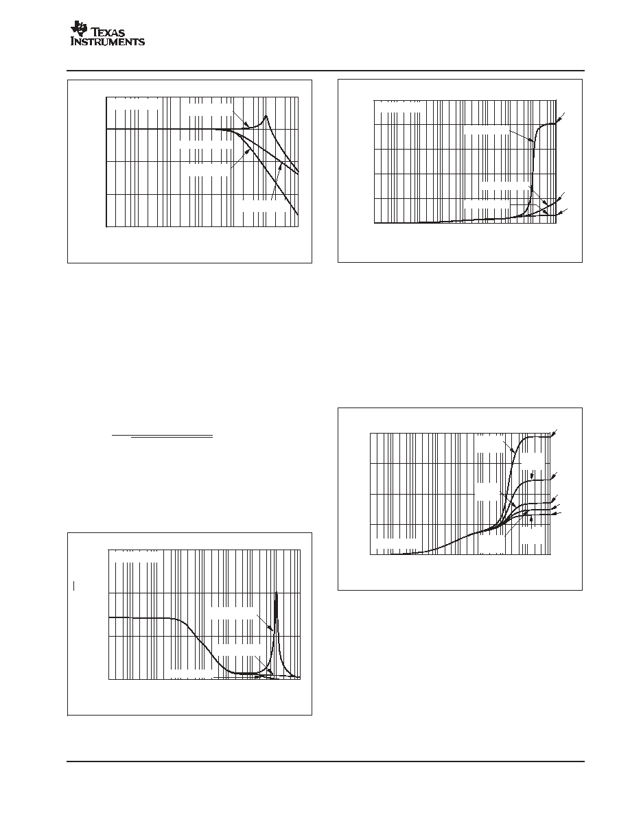
OFFSET VOLTAGE vs OUTPUT VOLTAGE
V
OUT
(V)
V
OS
(
µ
V)
0
1
2
3
4
5
V
S
= 5V
R
P
= 2k
connected to
-
5V
R
L
= 2k
connected to V
S
/2
Effect of clamp
Figure 2. Effect of high-speed overload recovery
clamp on output voltage
OVERLOAD RECOVERY
The OPA380 has been designed to prevent output
saturation. After being overdriven to the positive rail, it
will typically require only 100ns to return to linear
operation. The time required for negative overload
recovery is greater, unless a pulldown resistor
connected to a more negative supply is used to extend
the output swing all the way to the negative rail--see the
following section, Achieving Output Swing to Ground.
ACHIEVING OUTPUT SWING TO GROUND
Some applications require output voltage swing from
0V to a positive full-scale voltage (such as +4.096V)
with excellent accuracy. With most single-supply op
amps, problems arise when the output signal
approaches 0V, near the lower output swing limit of a
single-supply op amp. A good single-supply op amp
may swing close to single-supply ground, but will not
reach 0V.
The output of the OPA380 can be made to swing to
ground, or slightly below, on a single-supply power
source. This extended output swing requires the use of
another resistor and an additional negative power
supply. A pulldown resistor may be connected between
the output and the negative supply to pull the output
down to 0V. See Figure 3.
OPA380
V
OUT
R
F
R
P
= 2k
V+ = +5V
V
-
= Gnd
V
P
=
-
5V
Negative Supply
Figure 3. Amplifier with optional pull-down
resistor to achieve V
OUT
= 0V
The OPA380 has an output stage that allows the output
voltage to be pulled to its negative supply rail using this
technique. However, this technique only works with
some types of output stages. The OPA380 has been
designed to perform well with this method. Accuracy is
excellent down to 0V. Reliable operation is assured over
the specified temperature range.
OPA380
OPA2380
SBOS291E - NOVEMBER 2003 - REVISED NOVEMBER 2004
www.ti.com
11
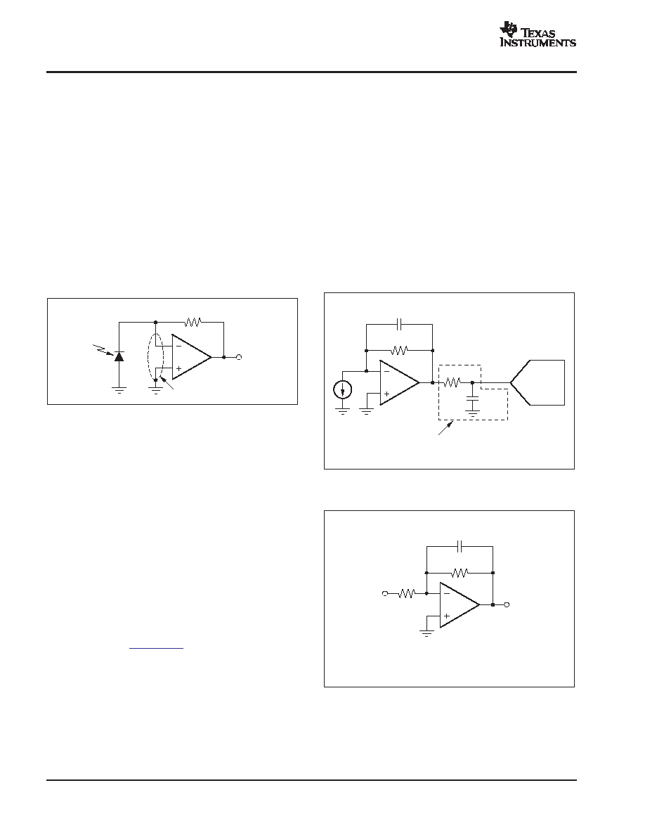
BIASING PHOTODIODES IN SINGLE-SUPPLY
CIRCUITS
The +IN input can be biased with a positive DC voltage
to offset the output voltage and allow the amplifier
output to indicate a true zero photodiode measurement
when the photodiode is not exposed to any light. It will
also prevent the added delay that results from coming
out of the negative rail. This bias voltage appears
across the photodiode, providing a reverse bias for
faster operation. An RC filter placed at this bias point will
reduce noise. (Refer to Figure 4.) This bias voltage can
also serve as an offset bias point for an ADC with range
that does not include ground.
OPA380
V
OUT
100k
V+
R
F
10M
C
F
(1)
< 1pF
0.1
µ
F
NOTE: (1) C
F
is optional to prevent gain peaking.
It includes the stray capacitance of R
F
.
+V
Bias
Figure 4. Filtered reverse bias voltage
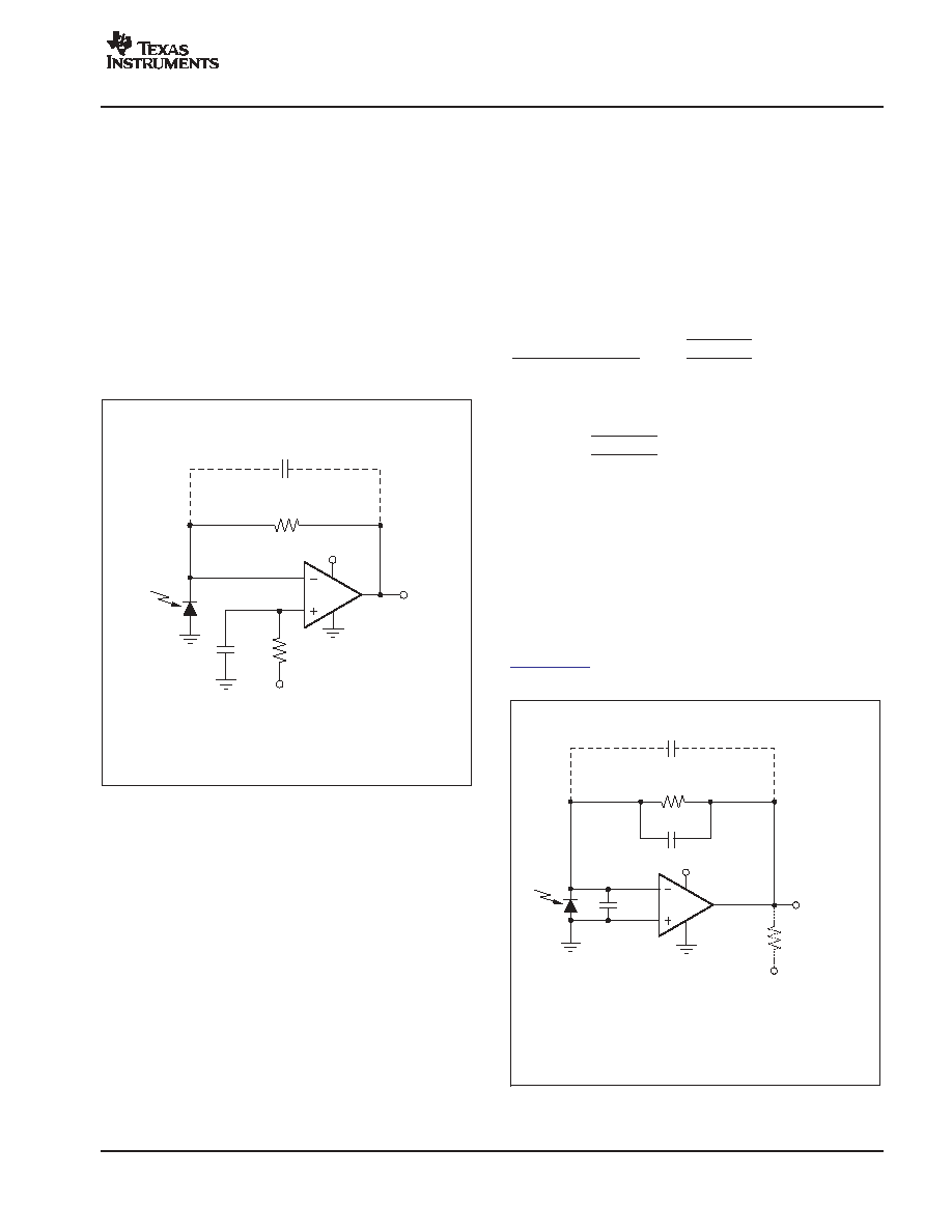
TRANSIMPEDANCE AMPLIFIER
Wide bandwidth, low input bias current, and low input
voltage and current noise make the OPA380 an ideal
wideband photodiode transimpedance amplifier. Low
voltage noise is important because photodiode
capacitance causes the effective noise gain of the
circuit to increase at high frequency.
The key elements to a transimpedance design are
shown in Figure 5:
the total input capacitance (C
TOT
), consisting of the
photodiode capacitance (C
DIODE
) plus the parasitic
common-mode and differential-mode input
capacitance (3pF + 1.1pF for the OPA380);
the desired transimpedance gain (R
F
);
the Gain Bandwidth Product (GBW) for the
OPA380 (90MHz).
With these three variables set, the feedback capacitor
value (C
F
) can be set to control the frequency response.
C
STRAY
is the stray capacitance of R
F
, which is 0.2pF for
a typical surface-mount resistor.
To achieve a maximally flat 2nd-order Butterworth
frequency response, the feedback pole should be set
to:
1
2
p
R
F
C
F
)
C
STRAY
+
GBW
4
p
R
F
C
TOT
Bandwidth is calculated by:
f
*
3dB
+
GBW
2
p
R
F
C
TOT
Hz
These equations will result in maximum
transimpedance bandwidth. For even higher
transimpedance bandwidth, the high-speed CMOS
OPA300 (180MHz GBW), or the OPA656 (230MHz
GBW) may be used.
For additional information, refer to Application Bulletin
AB-050 (SBOA055), Compensate Transimpedance
Amplifiers Intuitively, available for download at
www.ti.com
.
C
TOT
(3)
OPA380
V
OUT
-
5V
10M
+5V
R
F
C
F
(1)
C
STRAY
(2)
NOTE: (1) C
F
is optional to prevent gain peaking.
(2) C
STRAY
is the stray capacitance of R
F
(typically, 0.2pF for a surface-mount resistor).
(3) C
TOT
is the photodiode capacitance plus OPA380
input capacitance.
R
P
(optional
pulldown resistor)
Figure 5. Transimpedance Amplifier
(1)
(2)

OPA380
OPA2380
SBOS291E - NOVEMBER 2003 - REVISED NOVEMBER 2004
www.ti.com
12
TRANSIMPEDANCE BANDWIDTH AND
NOISE
Limiting the gain set by R
F
can decrease the noise
occurring at the output of the transimpedance circuit.
However, all required gain should occur in the
transimpedance stage, since adding gain after the
transimpedance amplifier generally produces poorer
noise performance. The noise spectral density
produced by R
F
increases with the square-root of R
F
,
whereas the signal increases linearly. Therefore,
signal-to-noise ratio is improved when all the required
gain is placed in the transimpedance stage.
Total noise increases with increased bandwidth. Limit
the circuit bandwidth to only that required. Use a
capacitor, C
F
, across the feedback resistor, R
F
, to limit
bandwidth, even if not required for stability if total output
noise is a concern.
Figure 6a shows the transimpedance circuit without any
feedback capacitor. The resulting transimpedance gain
of this circuit is shown in Figure 7. The ≠3dB point is
approximately 10MHz. Adding a 16pF feedback
capacitor (Figure 6b) will limit the bandwidth and result
in a ≠3dB point at approximately 1MHz (seen in
Figure 7). Output noise will be further reduced by
adding a filter (R
FILTER
and C
FILTER
) to create a second
pole (Figure 6c). This second pole is placed within the
feedback loop to maintain the amplifier's low output
impedance. (If the pole was placed outside the
feedback loop, an additional buffer would be required
and would inadvertently increase noise and dc error).
Using R
DIODE
to represent the equivalent diode
resistance, and C
TOT
for equivalent diode capacitance
plus OPA380 input capacitance, the noise zero, f
Z
, is
calculated by:
f
Z
+
R
DIODE
)
R
F
2
p
R
DIODE
R
F
C
TOT
)
C
F
OPA380
V
OUT
V
BIAS
R
F
= 10k
(a)
C
STRAY
= 0.2pF
C
F
= 16pF
OPA380
V
OUT
V
BIAS
R
F
= 10k
(b)
C
STRAY
= 0.2pF
V
OUT
C
FILTER
= 796pF
R
FILTER
= 100
C
F
= 21pF
OPA380
V
BIAS
R
F
= 10k
(c)
C
STRAY
= 0.2pF
Figure 6. Transimpedance circuit configurations
with varying total and integrated noise gain
(3)
OPA380
OPA2380
SBOS291E - NOVEMBER 2003 - REVISED NOVEMBER 2004
www.ti.com
13
110
80
50
20
-
10
Frequency (Hz)
Tr
a
n
s
i
m
p
e
d
a
n
c
e
Ga
i
n
(d
B
)
100
10k
1k
1M
10M
100k
100M
-
3dB BW at 1MHz
See Figure 6a
C
DIODE
= 10pF
See Figure 6c
See Figure 6b
Figure 7. Transimpedance gains for circuits in
Figure 6
The effect of these circuit configurations on output noise
is shown in Figure 8 and on integrated output noise in
Figure 9. A 2-pole Butterworth filter (maximally flat in
passband) is created by selecting the filter values using
the equation:
C
F
R
F
+
2C
FILTER
R
FILTER
with:
f
*
3dB
+
1
2
p
R
F
R
FILTER
C
F
C
FILTER
The circuit in Figure 6b rolls off at 20dB/decade. The
circuit with the additional filter shown in Figure 6c rolls
off at 40dB/decade, resulting in improved noise
performance.
300
200
100
0
Frequency (Hz)
O
u
tput
N
o
i
s
e
(
nV
/
Hz
)
C
DIODE
= 10pF
See Figure 6a
See Figure 6b
See Figure 6c
1
100
10
10k
1k
1M
10M
100k
100M
Figure 8. Output noise for circuits in Figure 6
500
400
300
200
100
0
Frequency (Hz)
1
100
10
10k
1k
1M
10M
100k
100M
419
µ
V
30
µ
V
86
µ
V
C
DIODE
= 10pF
See Figure 6a
See Figure 6b
See Figure 6c
Integrated
O
utput Noise
(
µ
V
rm
s
)
Figure 9. Integrated output noise for circuits in
Figure 6
Figure 10 shows the effect of diode capacitance on
integrated output noise, using the circuit in Figure 6c.
For additional information, refer to Noise Analysis of
FET Transimpedance Amplifiers (SBOA060), and
Noise Analysis for High Speed Op Amps (SBOA066),
available for download from the TI web site.
80
60
0
20
0
Frequency (Hz)
1
100
10
10k
1k
1M
10M
100k
100M
C
DIODE
= 100pF
C
DIODE
= 10pF
C
DIODE
= 1pF
See Figure 6c
C
DIODE
= 50pF
50
µ
V
35
µ
V
30
µ
V
27
µ
V
79
µ
V
C
DIODE
= 20pF
Integrated
Output Noise
(
µ
V
rm
s
)
Figure 10. Integrated output noise for various
values of C
DIODE
for circuit in Figure 6c
(4)
(5)
OPA380
OPA2380
SBOS291E - NOVEMBER 2003 - REVISED NOVEMBER 2004
www.ti.com
14
BOARD LAYOUT
Minimize photodiode capacitance and stray
capacitance at the summing junction (inverting input).
This capacitance causes the voltage noise of the op
amp to be amplified (increasing amplification at high
frequency). Using a low-noise voltage source to
reverse-bias a photodiode can significantly reduce its
capacitance. Smaller photodiodes have lower
capacitance. Use optics to concentrate light on a small
photodiode.
Circuit board leakage can degrade the performance of
an otherwise well-designed amplifier. Clean the circuit
board carefully. A circuit board guard trace that
encircles the summing junction and is driven at the
same voltage can help control leakage. See Figure 11.
Guard ring
R
F
V
OUT
OPA380
Figure 11. Connection of input guard
OTHER WAYS TO MEASURE SMALL
CURRENTS
Logarithmic amplifiers are used to compress extremely
wide dynamic range input currents to a much narrower
range. Wide input dynamic ranges of 8 decades, or
100pA to 10mA, can be accommodated for input to a
12-bit ADC. (Suggested products: LOG101, LOG102,
LOG104, LOG112.)
Extremely small currents can be accurately measured
by integrating currents on a capacitor. (Suggested
product: IVC102.)
Low-level currents can be converted to high-resolution
data words. (Suggested product: DDC112.)
For further information on the range of products
available, search
www.ti.com
using the above specific
model names or by using keywords transimpedance
and logarithmic.
CAPACITIVE LOAD AND STABILITY
The OPA380 series op amps can drive up to 500pF pure
capacitive load. Increasing the gain enhances the
amplifier's ability to drive greater capacitive loads (see
the Typical Characteristic curve, Small Signal
Overshoot vs Capacitive Load).
One method of improving capacitive load drive in the
unity-gain configuration is to insert a 10
to 20
resistor in series with the load. This reduces ringing with
large capacitive loads while maintaining DC accuracy.
DRIVING FAST 16-BIT ANALOG-TO-DIGITAL
CONVERTERS (ADC)
The OPA380 series is optimized for driving a fast 16-bit
ADC such as the ADS8411. The OPA380 op amp
buffers the converter's input capacitance and resulting
charge injection while providing signal gain. Figure 12
shows the OPA380 in a single-ended method of
interfacing the ADS8411 16-bit, 2MSPS ADC. For
additional information, refer to the ADS8411 data sheet.
OPA380
R
F
15
6800pF
ADS8411
C
F
RC Values shown are optimized for the
ADS8411
values may vary for other ADCs.
Figure 12. Driving 16-bit ADCs
OPA380
R
F
R
1
(Provides high-speed amplification
with very low offset and drift.)
V
OUT
C
F
V
IN
Figure 13. OPA380 inverting gain configuration

PACKAGING INFORMATION
Orderable Device
Status
(1)
Package
Type
Package
Drawing
Pins Package
Qty
Eco Plan
(2)
Lead/Ball Finish
MSL Peak Temp
(3)
OPA2380AIDGKR
ACTIVE
MSOP
DGK
8
2500 Green (RoHS &
no Sb/Br)
CU NIPDAU
Level-2-260C-1 YEAR
OPA2380AIDGKT
ACTIVE
MSOP
DGK
8
250
Green (RoHS &
no Sb/Br)
CU NIPDAU
Level-2-260C-1 YEAR
OPA380AID
ACTIVE
SOIC
D
8
100
None
CU SNPB
Level-1-220C-UNLIM
OPA380AIDGKR
ACTIVE
MSOP
DGK
8
2500
None
CU NIPDAU
Level-1-220C-UNLIM
OPA380AIDGKT
ACTIVE
MSOP
DGK
8
250
None
CU NIPDAU
Level-1-220C-UNLIM
OPA380AIDR
ACTIVE
SOIC
D
8
2500
None
CU SNPB
Level-1-220C-UNLIM
(1)
The marketing status values are defined as follows:
ACTIVE: Product device recommended for new designs.
LIFEBUY: TI has announced that the device will be discontinued, and a lifetime-buy period is in effect.
NRND: Not recommended for new designs. Device is in production to support existing customers, but TI does not recommend using this part in
a new design.
PREVIEW: Device has been announced but is not in production. Samples may or may not be available.
OBSOLETE: TI has discontinued the production of the device.
(2)
Eco Plan - May not be currently available - please check
http://www.ti.com/productcontent
for the latest availability information and additional
product content details.
None: Not yet available Lead (Pb-Free).
Pb-Free (RoHS): TI's terms "Lead-Free" or "Pb-Free" mean semiconductor products that are compatible with the current RoHS requirements
for all 6 substances, including the requirement that lead not exceed 0.1% by weight in homogeneous materials. Where designed to be soldered
at high temperatures, TI Pb-Free products are suitable for use in specified lead-free processes.
Green (RoHS & no Sb/Br): TI defines "Green" to mean "Pb-Free" and in addition, uses package materials that do not contain halogens,
including bromine (Br) or antimony (Sb) above 0.1% of total product weight.
(3)
MSL, Peak Temp. -- The Moisture Sensitivity Level rating according to the JEDECindustry standard classifications, and peak solder
temperature.
Important Information and Disclaimer:The information provided on this page represents TI's knowledge and belief as of the date that it is
provided. TI bases its knowledge and belief on information provided by third parties, and makes no representation or warranty as to the
accuracy of such information. Efforts are underway to better integrate information from third parties. TI has taken and continues to take
reasonable steps to provide representative and accurate information but may not have conducted destructive testing or chemical analysis on
incoming materials and chemicals. TI and TI suppliers consider certain information to be proprietary, and thus CAS numbers and other limited
information may not be available for release.
In no event shall TI's liability arising out of such information exceed the total purchase price of the TI part(s) at issue in this document sold by TI
to Customer on an annual basis.
PACKAGE OPTION ADDENDUM
www.ti.com
9-Dec-2004
Addendum-Page 1


IMPORTANT NOTICE
Texas Instruments Incorporated and its subsidiaries (TI) reserve the right to make corrections, modifications,
enhancements, improvements, and other changes to its products and services at any time and to discontinue
any product or service without notice. Customers should obtain the latest relevant information before placing
orders and should verify that such information is current and complete. All products are sold subject to TI's terms
and conditions of sale supplied at the time of order acknowledgment.
TI warrants performance of its hardware products to the specifications applicable at the time of sale in
accordance with TI's standard warranty. Testing and other quality control techniques are used to the extent TI
deems necessary to support this warranty. Except where mandated by government requirements, testing of all
parameters of each product is not necessarily performed.
TI assumes no liability for applications assistance or customer product design. Customers are responsible for
their products and applications using TI components. To minimize the risks associated with customer products
and applications, customers should provide adequate design and operating safeguards.
TI does not warrant or represent that any license, either express or implied, is granted under any TI patent right,
copyright, mask work right, or other TI intellectual property right relating to any combination, machine, or process
in which TI products or services are used. Information published by TI regarding third-party products or services
does not constitute a license from TI to use such products or services or a warranty or endorsement thereof.
Use of such information may require a license from a third party under the patents or other intellectual property
of the third party, or a license from TI under the patents or other intellectual property of TI.
Reproduction of information in TI data books or data sheets is permissible only if reproduction is without
alteration and is accompanied by all associated warranties, conditions, limitations, and notices. Reproduction
of this information with alteration is an unfair and deceptive business practice. TI is not responsible or liable for
such altered documentation.
Resale of TI products or services with statements different from or beyond the parameters stated by TI for that
product or service voids all express and any implied warranties for the associated TI product or service and
is an unfair and deceptive business practice. TI is not responsible or liable for any such statements.
Following are URLs where you can obtain information on other Texas Instruments products and application
solutions:
Products
Applications
Amplifiers
amplifier.ti.com
Audio
www.ti.com/audio
Data Converters
dataconverter.ti.com
Automotive
www.ti.com/automotive
DSP
dsp.ti.com
Broadband
www.ti.com/broadband
Interface
interface.ti.com
Digital Control
www.ti.com/digitalcontrol
Logic
logic.ti.com
Military
www.ti.com/military
Power Mgmt
power.ti.com
Optical Networking
www.ti.com/opticalnetwork
Microcontrollers
microcontroller.ti.com
Security
www.ti.com/security
Telephony
www.ti.com/telephony
Video & Imaging
www.ti.com/video
Wireless
www.ti.com/wireless
Mailing Address:
Texas Instruments
Post Office Box 655303 Dallas, Texas 75265
Copyright
2004, Texas Instruments Incorporated