 | –≠–ª–µ–∫—Ç—Ä–æ–Ω–Ω—ã–π –∫–æ–º–ø–æ–Ω–µ–Ω—Ç: OPA134PA | –°–∫–∞—á–∞—Ç—å:  PDF PDF  ZIP ZIP |
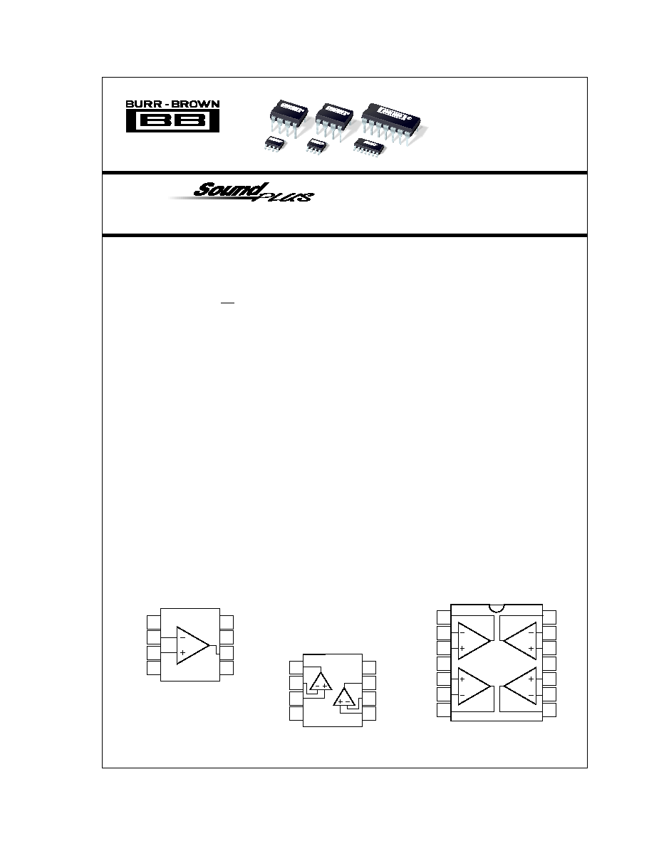
FEATURES
q
SUPERIOR SOUND QUALITY
q
ULTRA LOW DISTORTION: 0.00008%
q
LOW NOISE: 8nV/
Hz
q
TRUE FET-INPUT: I
B
= 5pA
q
HIGH SPEED:
SLEW RATE: 20V/
µ
s
BANDWIDTH: 8MHz
q
HIGH OPEN-LOOP GAIN: 120dB (600
)
q
WIDE SUPPLY RANGE:
±
2.5V to
±
18V
q
SINGLE, DUAL, AND QUAD VERSIONS
High Performance
AUDIO OPERATIONAL AMPLIFIERS
TM
DESCRIPTION
The OPA134 series are ultra-low distortion, low noise
operational amplifiers fully specified for audio appli-
cations. A true FET input stage was incorporated to
provide superior sound quality and speed for excep-
tional audio performance. This in combination with
high output drive capability and excellent dc perfor-
mance allows use in a wide variety of demanding
applications. In addition, the OPA134's wide output
swing, to within 1V of the rails, allows increased
headroom making it ideal for use in any audio circuit.
OPA134 op amps are easy to use and free from phase
inversion and overload problems often found in com-
mon FET-input op amps. They can be operated from
±
2.5V to
±
18V power supplies. Input cascode cir-
cuitry provides excellent common-mode rejection and
maintains low input bias current over its wide input
voltage range, minimizing distortion. OPA134 series
op amps are unity-gain stable and provide excellent
dynamic behavior over a wide range of load condi-
tions, including high load capacitance. The dual and
quad versions feature completely independent cir-
cuitry for lowest crosstalk and freedom from interac-
tion, even when overdriven or overloaded.
Single and dual versions are available in 8-pin DIP
and SO-8 surface-mount packages in standard con-
figurations. The quad is available in 14-pin DIP and
SO-14 surface mount packages. All are specified for
≠40
∞
C to +85
∞
C operation. A SPICE macromodel is
available for design analysis.
APPLICATIONS
q
PROFESSIONAL AUDIO AND MUSIC
q
LINE DRIVERS
q
LINE RECEIVERS
q
MULTIMEDIA AUDIO
q
ACTIVE FILTERS
q
PREAMPLIFIERS
q
INTEGRATORS
q
CROSSOVER NETWORKS
© 1996 Burr-Brown Corporation
PDS-1339C
Printed in U.S.A. December, 1997
International Airport Industrial Park ∑ Mailing Address: PO Box 11400, Tucson, AZ 85734 ∑ Street Address: 6730 S. Tucson Blvd., Tucson, AZ 85706 ∑ Tel: (520) 746-1111 ∑ Twx: 910-952-1111
Internet: http://www.burr-brown.com/ ∑ FAXLine: (800) 548-6133 (US/Canada Only) ∑ Cable: BBRCORP ∑ Telex: 066-6491 ∑ FAX: (520) 889-1510 ∑ Immediate Product Info: (800) 548-6132
1
2
3
4
8
7
6
5
V+
Out B
≠In B
+In B
Out A
≠In A
+In A
V≠
OPA2134
8-Pin DIP, SO-8
A
B
1
2
3
4
5
6
7
14
13
12
11
10
9
8
Out D
≠In D
+In D
V≠
+In C
≠In C
Out C
Out A
≠In A
+In A
V+
+In B
≠In B
Out B
OPA4134
14-Pin DIP
SO-14
A
D
B
C
1
2
3
4
8
7
6
5
Offset Trim
V+
Output
NC
Offset Trim
≠In
+In
V≠
OPA134
8-Pin DIP, SO-8
Æ
OPA134
OPA2134
OPA4134
OPA134
OPA2134
OPA4134
OPA4134
OPA134
OPA2134
2
Æ
OPA134/2134/4134
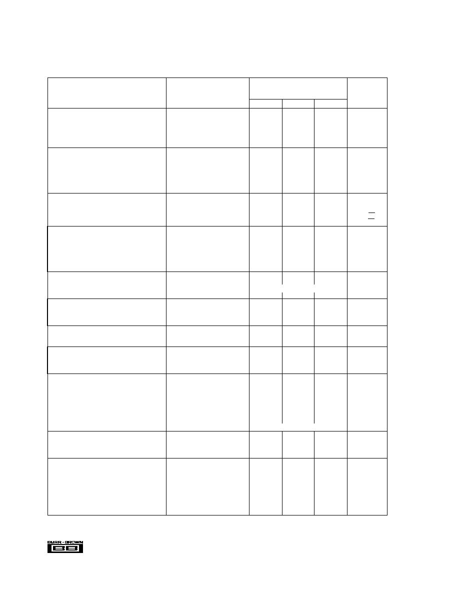
SPECIFICATIONS
At T
A
= +25
∞
C, V
S
=
±
15V, unless otherwise noted.
OPA134PA, UA
OPA2134PA, UA
OPA4134PA, UA
PARAMETER
CONDITION
MIN
TYP
MAX
UNITS
AUDIO PERFORMANCE
Total Harmonic Distortion + Noise
G = 1, f = 1kHz, V
O
= 3Vrms
R
L
= 2k
0.00008
%
R
L
= 600
0.00015
%
Intermodulation Distortion
G = 1, f = 1kHz, V
O
= 1Vp-p
≠98
dB
Headroom
(1)
THD < 0.01%, R
L
= 2k
, V
S
=
±
18V
23.6
dBu
FREQUENCY RESPONSE
Gain-Bandwidth Product
8
MHz
Slew Rate
(2)
±
15
±
20
V/
µ
s
Full Power Bandwidth
1.3
MHz
Settling Time 0.1%
G = 1, 10V Step, C
L
= 100pF
0.7
µ
s
0.01%
G = 1, 10V Step, C
L
= 100pF
1
µ
s
Overload Recovery Time
(V
IN
) ∑ (Gain) = V
S
0.5
µ
s
NOISE
Input Voltage Noise
Noise Voltage, f = 20Hz to 20kHz
1.2
µ
Vrms
Noise Density, f = 1kHz
8
nV/
Hz
Current Noise Density, f = 1kHz
3
fA/
Hz
OFFSET VOLTAGE
Input Offset Voltage
±
0.5
±
2
mV
T
A
= ≠40
∞
C to +85
∞
C
±
1
±
3
(3)
mV
vs Temperature
T
A
= ≠40
∞
C to +85
∞
C
±
2
µ
V/
∞
C
vs Power Supply (PSRR)
V
S
=
±
2.5V to
±
18V
90
106
dB
Channel Separation (Dual, Quad)
dc, R
L
= 2k
135
dB
f = 20kHz, R
L
= 2k
130
dB
INPUT BIAS CURRENT
Input Bias Current
(4)
V
CM
=0V
+5
±
100
pA
vs Temperature
(3)
See Typical Curve
±
5
nA
Input Offset Current
(4)
V
CM
=0V
±
2
±
50
pA
INPUT VOLTAGE RANGE
Common-Mode Voltage Range
(V≠)+2.5
±
13
(V+)≠2.5
V
Common-Mode Rejection
V
CM
= ≠12.5V to +12.5V
86
100
dB
T
A
= ≠40
∞
C to +85
∞
C
90
dB
INPUT IMPEDANCE
Differential
10
13
|| 2
|| pF
Common-Mode
V
CM
= ≠12.5V to +12.5V
10
13
|| 5
|| pF
OPEN-LOOP GAIN
Open-Loop Voltage Gain
R
L
= 10k
, V
O
= ≠14.5V to +13.8V
104
120
dB
R
L
= 2k
, V
O
= ≠13.8V to +13.5V
104
120
dB
R
L
= 600
, V
O
= ≠12.8V to +12.5V
104
120
dB
OUTPUT
Voltage Output
R
L
= 10k
(V≠)+0.5
(V+)≠1.2
V
R
L
= 2k
(V≠)+1.2
(V+)≠1.5
V
R
L
= 600
(V≠)+2.2
(V+)≠2.5
V
Output Current
±
35
mA
Output Impedance, Closed-Loop
(5)
f = 10kHz
0.01
Open-Loop
f = 10kHz
10
Short-Circuit Current
±
40
mA
Capacitive Load Drive (Stable Operation)
See Typical Curve
POWER SUPPLY
Specified Operating Voltage
±
15
V
Operating Voltage Range
±
2.5
±
18
V
Quiescent Current (per amplifier)
I
O
= 0
4
5
mA
TEMPERATURE RANGE
Specified Range
≠40
+85
∞
C
Operating Range
≠55
+125
∞
C
Storage
≠55
+125
∞
C
Thermal Resistance,
JA
8-Pin DIP
100
∞
C/W
SO-8 Surface-Mount
150
∞
C/W
14-Pin DIP
80
∞
C/W
SO-14 Surface-Mount
110
∞
C/W
NOTES: (1) dBu = 20*log (Vrms/0.7746) where Vrms is the maximum output voltage for which THD+Noise is less than 0.01%. See THD+Noise text. (2) Guaranteed
by design. (3) Guaranteed by wafer-level test to 95% confidence level. (4) High-speed test at T
J
= 25
∞
C. (5) See "Closed-Loop Output Impedance vs Frequency"
typical curve.
3
OPA134/2134/4134
Æ
PACKAGE
DRAWING
TEMPERATURE
PRODUCT
PACKAGE
NUMBER
(1)
RANGE
Single
OPA134PA
8-Pin Plastic DIP
006
≠40
∞
C to +85
∞
C
OPA134UA
SO-8 Surface-Mount
182
≠40
∞
C to +85
∞
C
Dual
OPA2134PA
8-Pin Plastic DIP
006
≠40
∞
C to +85
∞
C
OPA2134UA
SO-8 Surface-Mount
182
≠40
∞
C to +85
∞
C
Quad
OPA4134PA
14-Pin Plastic DIP
010
≠40
∞
C to +85
∞
C
OPA4134UA
SO-14 Surface-Mount
235
≠40
∞
C to +85
∞
C
NOTE: (1) For detailed drawing and dimension table, please see end of data
sheet, or Appendix C of Burr-Brown IC Data Book.
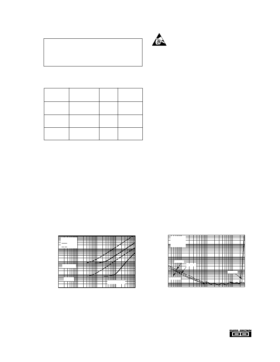
ELECTROSTATIC
DISCHARGE SENSITIVITY
This integrated circuit can be damaged by ESD. Burr-Brown
recommends that all integrated circuits be handled with
appropriate precautions. Failure to observe proper handling
and installation procedures can cause damage.
ESD damage can range from subtle performance degrada-
tion to complete device failure. Precision integrated circuits
may be more susceptible to damage because very small
parametric changes could cause the device not to meet its
published specifications.
ABSOLUTE MAXIMUM RATINGS
(1)
Supply Voltage, V+ to V≠ .................................................................... 36V
Input Voltage .................................................... (V≠) ≠0.7V to (V+) +0.7V
Output Short-Circuit
(2)
.............................................................. Continuous
Operating Temperature ................................................. ≠40
∞
C to +125
∞
C
Storage Temperature ..................................................... ≠55
∞
C to +125
∞
C
Junction Temperature ...................................................................... 150
∞
C
Lead Temperature (soldering, 10s) ................................................. 300
∞
C
NOTES: (1) Stresses above these ratings may cause permanent damage.
(2) Short-circuit to ground, one amplifier per package.
TYPICAL PERFORMANCE CURVES
At T
A
= +25
∞
C, V
S
=
±
15V, R
L
= 2k
, unless otherwise noted.
TOTAL HARMONIC DISTORTION + NOISE
vs FREQUENCY
Frequency (Hz)
THD+Noise (%)
0.1
0.01
0.001
0.0001
0.00001
10
100
1k
10k
100k
2k
600
R
L
V
O
= 3Vrms
G = +1
G = +10
SMPTE INTERMODULATION DISTORTION
vs OUTPUT AMPLITUDE
Output Amplitude (Vpp)
IMD (%)
1
0.1
0.010
0.001
0.0005
5
30m
0.1
1
10
30
G = +1
f = 1kHz
R
L
= 2k
Baseline
OP176
OPA134
OPA134
The information provided herein is believed to be reliable; however, BURR-BROWN assumes no responsibility for inaccuracies or omissions. BURR-BROWN assumes
no responsibility for the use of this information, and all use of such information shall be entirely at the user's own risk. Prices and specifications are subject to change
without notice. No patent rights or licenses to any of the circuits described herein are implied or granted to any third party. BURR-BROWN does not authorize or warrant
any BURR-BROWN product for use in life support devices and/or systems.
PACKAGE/ORDERING INFORMATION
4
Æ
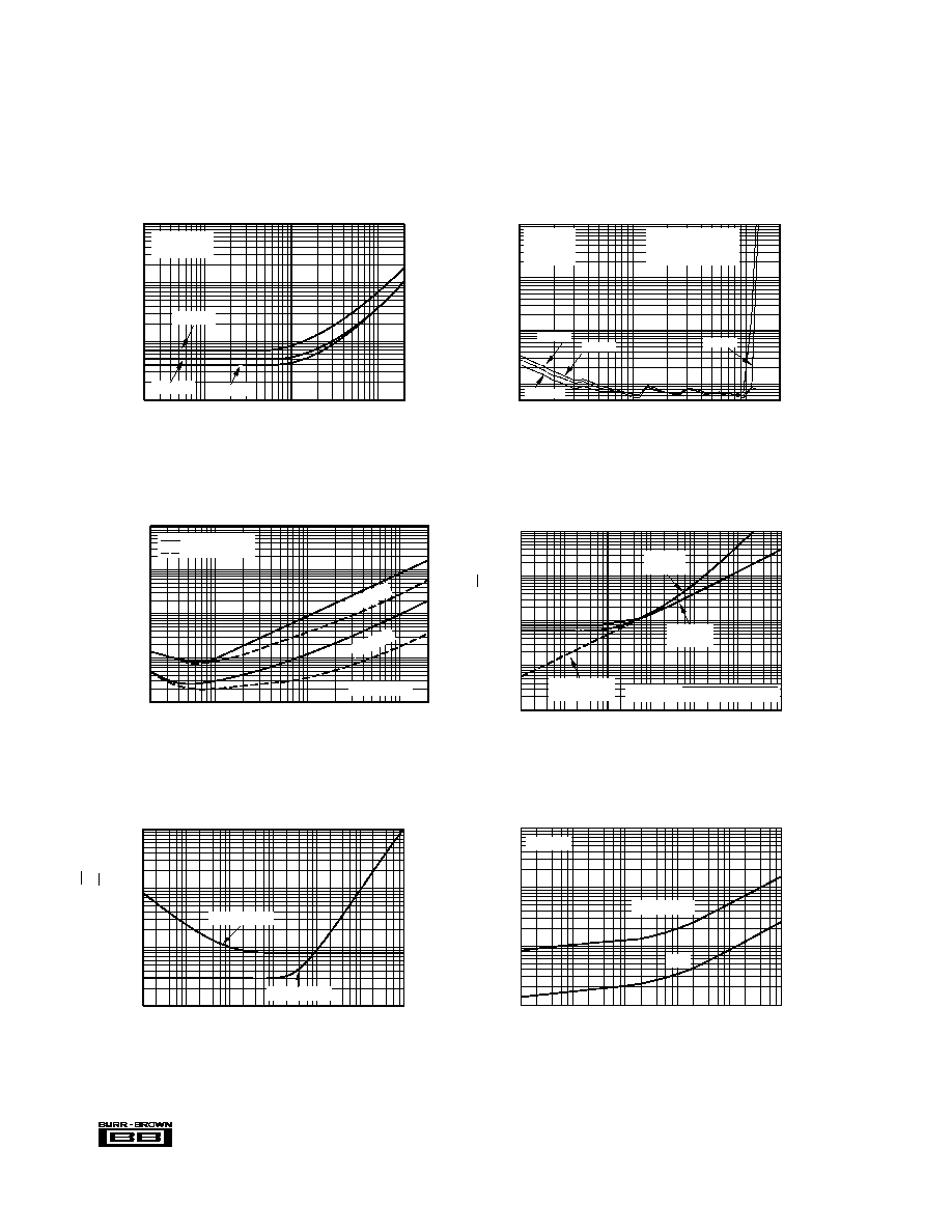
OPA134/2134/4134
HEADROOM ≠ TOTAL HARMONIC DISTORTION
+ NOISE vs OUTPUT AMPLITUDE
Output Amplitude (Vrms)
THD+Noise (%)
1
0.1
0.010
0.001
0.0005
0.1
1
10
20
V
S
= ±18V
R
L
= 2k
f = 1kHz
THD < 0.01%
OPA134 ≠ 11.7Vrms
OP176 ≠ 11.1Vrms
Baseline
OP176
OPA134
OPA134
TYPICAL PERFORMANCE CURVES
(CONT)
At T
A
= +25
∞
C, V
S
=
±
15V, R
L
= 2k
, unless otherwise noted.
TOTAL HARMONIC DISTORTION + NOISE
vs FREQUENCY
Frequency (Hz)
THD+Noise (%)
0.01
0.001
0.0001
0.00001
20
100
1k
10k
20k
V
O
= 10Vrms
R
L
= 2k
V
S
= ±16
V
S
= ±17
V
S
= ±18
HARMONIC DISTORTION + NOISE vs FREQUENCY
Frequency (Hz)
Amplitude (% of Fundamentals)
0.01
0.001
0.0001
0.00001
0.000001
20
100
1k
10k
20k
2nd Harmonic
3rd Harmonic
V
O
= 1Vrms
R
L
= 600
R
L
= 2k
VOLTAGE NOISE vs SOURCE RESISTANCE
Source Resistance (
)
Voltage Noise (nV/
Hz)
1k
100
10
1
0.1
10
100
1k
10k
100k
1M
10M
OP176+
Resistor
OPA134+
Resistor
Resistor Noise
Only
V
n
(total) =
(i
n
R
S
)
2
+ e
n
2
+ 4kTR
S
INPUT VOLTAGE AND CURRENT NOISE
SPECTRAL DENSITY vs FREQUENCY
1
1k
100
10
Voltage Noise (nV/
Hz)
Frequency (Hz)
10
100
1k
10k
100k
1M
1
Current Noise (fA/
Hz)
Voltage Noise
Current Noise
INPUT-REFERRED NOISE VOLTAGE
vs NOISE BANDWIDTH
Noise Bandwidth (Hz)
Noise Voltage (
µ
V)
100
10
1
0.1
1
10
100
1k
10k
100k
R
S
= 20
Peak-to-Peak
RMS
5
OPA134/2134/4134
Æ
TYPICAL PERFORMANCE CURVES
(CONT)
At T
A
= +25
∞
C, V
S
=
±
15V, R
L
= 2k
, unless otherwise noted.
OPEN-LOOP GAIN/PHASE vs FREQUENCY
0.1
1
10
100
1k
10k
100k
1M
10M
160
140
120
100
80
60
40
20
0
≠20
0
≠45
≠90
≠135
≠180
Voltage Gain (dB)
Phase Shift (∞)
Frequency (Hz)
G
CLOSED-LOOP GAIN vs FREQUENCY
Frequency (Hz)
Closed-Loop Gain (dB)
50
40
30
20
10
0
≠10
≠20
1k
10k
100k
1M
10M
G = +10
G = +100
G = +1
POWER SUPPLY AND COMMON-MODE REJECTION
vs FREQUENCY
Frequency (Hz)
PSR, CMR (dB)
120
100
80
60
40
20
0
10
100
1k
10k
100k
1M
CMR
≠PSR
+PSR
MAXIMUM OUTPUT VOLTAGE
vs FREQUENCY
Frequency (Hz)
10k
100k
1M
10M
30
20
10
0
Output Voltage (Vp-p)
V
S
= ±15V
V
S
= ±2.5V
V
S
= ±5V
Maximum output voltage
without slew-rate
induced distortion
CLOSED-LOOP OUTPUT IMPEDANCE vs FREQUENCY
Frequency (Hz)
Closed-Loop Output Impedance (
)
10
1
0.1
0.01
0.001
0.0001
10
100
1k
10k
100k
G = +1
G = +2
G = +10
G = +100
Note: Open-Loop
Output Impedance
at f = 10kHz is 10
CHANNEL SEPARATION vs FREQUENCY
Frequency (Hz)
Channel Separation (dB)
160
140
120
100
80
100
1k
10k
100k
Dual and quad devices.
G = 1, all channels.
Quad measured channel
A to D or B to C--other
combinations yield improved
rejection.
R
L
=
R
L
= 2k
6
Æ
OPA134/2134/4134
FPO
TYPICAL PERFORMANCE CURVES
(CONT)
At T
A
= +25
∞
C, V
S
=
±
15V, R
L
= 2k
, unless otherwise noted.
INPUT BIAS CURRENT vs TEMPERATURE
Ambient Temperature (∞C)
Input Bias Current (pA)
100k
10k
1k
100
10
1
0.1
≠75
≠50
≠25
0
25
50
75
100
125
Dual
Single
High Speed Test
Warmed Up
INPUT BIAS CURRENT
vs INPUT COMMON-MODE VOLTAGE
Common-Mode Voltage (V)
Input Bias Current (pA)
10
9
8
7
6
5
4
3
2
1
0
≠15
≠10
≠5
0
5
10
15
High Speed Test
OPEN-LOOP GAIN vs TEMPERATURE
150
140
130
120
110
100
Open-Loop Gain (dB)
Temperature (∞C)
≠75
≠50
≠25
0
25
50
75
100
125
R
L
= 600
R
L
= 2k
R
L
= 10k
CMR, PSR vs TEMPERATURE
Ambient Temperature (∞C)
CMR, PSR (dB)
120
110
100
90
≠75
≠50
≠25
0
25
50
75
100
125
PSR
CMR
QUIESCENT CURRENT AND SHORT-CIRCUIT CURRENT
vs TEMPERATURE
Ambient Temperature (∞C)
Quiescent Current Per Amp (mA)
4.3
4.2
4.1
4.0
3.9
3.8
60
50
40
30
20
10
Short-Circuit Current (mA)
≠75
≠50
≠25
0
25
50
75
100
125
±I
SC
±I
Q
OUTPUT VOLTAGE SWING vs OUTPUT CURRENT
15
14
13
12
11
10
≠10
≠11
≠12
≠13
≠14
≠15
0
10
20
30
40
50
60
Output Current (mA)
Output Voltage Swing (V)
≠55∞C
≠55∞C
25∞C
25∞C
85∞C
85∞C
125∞C
125∞C
25∞C
V
IN
= ≠15V
V
IN
= 15V

7
OPA134/2134/4134
Æ
TYPICAL PERFORMANCE CURVES
(CONT)
At T
A
= +25
∞
C, V
S
=
±
15V, R
L
= 2k
, unless otherwise noted.
SMALL-SIGNAL STEP RESPONSE
G =1, C
L
= 100pF
200ns/div
50mV/div
LARGE-SIGNAL STEP RESPONSE
G = 1, C
L
= 100pF
5V/div
1µs/div
SETTLING TIME vs CLOSED-LOOP GAIN
Closed-Loop Gain (V/V)
Settling Time (µs)
100
10
1
0.1
±1
±10
±100
±1000
0.01%
0.1%
SMALL-SIGNAL OVERSHOOT
vs LOAD CAPACITANCE
60
50
40
30
20
10
0
100pF
1nF
10nF
Load Capacitance
Overshoot (%)
G = +1
G = ±10
G = ≠1
OFFSET VOLTAGE PRODUCTION DISTRIBUTION
Percent of Amplifiers (%)
Offset Voltage (V)
≠2000
≠1800
≠1600
≠1400
≠1200
≠1000
≠800
≠600
≠400
≠200
0
200
400
600
800
1000
1200
1400
1600
1800
2000
18
16
14
12
10
8
6
4
2
0
Typical production
distribution of packaged
units.
OFFSET VOLTAGE DRIFT
PRODUCTION DISTRIBUTION
Percent of Amplifiers (%)
Offset Voltage Drift (µV/∞C)
0.5
1.5
2.5
3.5
4.5
5.5
6.5
7.5
8.5
9.5
10.5
11.5
12.5
12
10
8
6
4
2
0
Typical production
distribution of packaged
units.
8
Æ
OPA134/2134/4134
APPLICATIONS INFORMATION
OPA134 series op amps are unity-gain stable and suitable
for a wide range of audio and general-purpose applications.
All circuitry is completely independent in the dual version,
assuring normal behavior when one amplifier in a package
is overdriven or short-circuited. Power supply pins should
be bypassed with 10nF ceramic capacitors or larger to
minimize power supply noise.
OPERATING VOLTAGE
OPA134 series op amps operate with power supplies from
±
2.5V to
±
18V with excellent performance. Although
specifications are production tested with
±
15V supplies,
most behavior remains unchanged throughout the full
operating voltage range. Parameters which vary signifi-
cantly with operating voltage are shown in the typical
performance curves.
OFFSET VOLTAGE TRIM
Offset voltage of OPA134 series amplifiers is laser trimmed
and usually requires no user adjustment. The OPA134
(single op amp version) provides offset trim connections
on pins 1 and 8, identical to 5534 amplifiers. Offset
voltage can be adjusted by connecting a potentiometer as
shown in Figure 1. This adjustment should be used only to
null the offset of the op amp, not to adjust system offset or
offset produced by the signal source. Nulling offset could
change the offset voltage drift behavior of the op amp.
While it is not possible to predict the exact change in drift,
the effect is usually small.
TOTAL HARMONIC DISTORTION
OPA134 series op amps have excellent distortion character-
istics. THD+Noise is below 0.0004% throughout the audio
frequency range, 20Hz to 20kHz, with a 2k
load. In
addition, distortion remains relatively flat through its
wide output voltage swing range, providing increased head-
room compared to other audio amplifiers, including the
OP176/275.
FIGURE 1. OPA134 Offset Voltage Trim Circuit.
V+
V≠
100k
OPA134 single op amp only.
Use offset adjust pins only to null
offset voltage of op amp--see text.
Trim Range: ±4mV typ
OPA134
6
7
8
4
3
2
1
10nF
10nF
In many ways headroom is a subjective measurement. It can
be thought of as the maximum output amplitude allowed
while still maintaining a very low level of distortion. In an
attempt to quantify headroom, we have defined "very low
distortion" as 0.01%. Headroom is expressed as a ratio
which compares the maximum allowable output voltage
level to a standard output level (1mW into 600
, or
0.7746Vrms). Therefore, OPA134 series op amps, which
have a maximum allowable output voltage level of 11.7Vrms
(THD+Noise < 0.01%), have a headroom specification of
23.6dBu. See the typical curve "Headroom - Total Harmonic
Distortion + Noise vs Output Amplitude."
DISTORTION MEASUREMENTS
The distortion produced by OPA134 series op amps is below
the measurement limit of all known commercially available
equipment. However, a special test circuit can be used to
extend the measurement capabilities.
Op amp distortion can be considered an internal error source
which can be referred to the input. Figure 2 shows a
circuit which causes the op amp distortion to be 101 times
greater than normally produced by the op amp. The addition
of R
3
to the otherwise standard non-inverting amplifier
FIGURE 2. Distortion Test Circuit.
R
2
OPA134
R
1
Signal Gain = 1+
Distortion Gain = 1+
R
3
V
O
= 3Vrms
Generator
Output
Analyzer
Input
Audio Precision
System One
Analyzer
(1)
R
L
1k
IBM PC
or
Compatible
SIG.
GAIN
DIST.
GAIN
R
1
R
2
R
3
100
10
1k
1k
1k
10
11
1
11
101
101
101
101
NOTE: (1) Measurement BW = 80kHz
R
2
R
1
R
2
R
1
II R
3

9
OPA134/2134/4134
Æ
V
OUT
V
IN
R
1
If R
S
> 2k
or R
1
II R
2
> 2k
R
S
= R
1
II R
2
R
2
OPA134
configuration alters the feedback factor or noise gain of the
circuit. The closed-loop gain is unchanged, but the feedback
available for error correction is reduced by a factor of 101,
thus extending the resolution by 101. Note that the input
signal and load applied to the op amp are the same as with
conventional feedback without R
3
. The value of R
3
should
be kept small to minimize its effect on the distortion mea-
surements.
Validity of this technique can be verified by duplicating
measurements at high gain and/or high frequency where the
distortion is within the measurement capability of the test
equipment. Measurements for this data sheet were made
with an Audio Precision distortion/noise analyzer which
greatly simplifies such repetitive measurements. The mea-
surement technique can, however, be performed with manual
distortion measurement instruments.
SOURCE IMPEDANCE AND DISTORTION
For lowest distortion with a source or feedback network
which has an impedance greater than 2k
, the impedance
seen by the positive and negative inputs in noninverting
applications should be matched. The p-channel JFETs in the
FET input stage exhibit a varying input capacitance with
applied common-mode input voltage. In inverting configu-
rations the input does not vary with input voltage since the
inverting input is held at virtual ground. However, in
noninverting applications the inputs do vary, and the gate-
to-source voltage is not constant. The effect is increased
distortion due to the varying capacitance for unmatched
source impedances greater than 2k
.
To maintain low distortion, match unbalanced source im-
pedance with appropriate values in the feedback network as
shown in Figure 3. Of course, the unbalanced impedance
may be from gain-setting resistors in the feedback path. If
the parallel combination of R
1
and R
2
is greater than 2k
, a
matching impedance on the noninverting input should be
used. As always, resistor values should be minimized to
reduce the effects of thermal noise.
FIGURE 3. Impedance Matching for Maintaining Low
Distortion in Non-Inverting Circuits.
NOISE PERFORMANCE
Circuit noise is determined by the thermal noise of external
resistors and op amp noise. Op amp noise is described by
two parameters--noise voltage and noise current. The total
noise is quantified by the equation:
With low source impedance, the current noise term is
insignificant and voltage noise dominates the noise perfor-
mance. At high source impedance, the current noise term
becomes the dominant contributor.
Low noise bipolar op amps such as the OPA27 and OPA37
provide very low voltage noise at the expense of a higher
current noise. However, OPA134 series op amps are unique
in providing very low voltage noise and very low current
noise. This provides optimum noise performance over a
wide range of sources, including reactive source imped-
ances, refer to the typical curve, "Voltage Noise vs Source
Resistance." Above 2k
source resistance, the op amp
contributes little additional noise--the voltage and current
terms in the total noise equation become insignificant and
the source resistance term dominates. Below 2k
, op amp
voltage noise dominates over the resistor noise, but com-
pares favorably with other audio op amps such as OP176.
PHASE REVERSAL PROTECTION
OPA134 series op amps are free from output phase-reversal
problems. Many audio op amps, such as OP176, exhibit
phase-reversal of the output when the input common-mode
voltage range is exceeded. This can occur in voltage-fol-
lower circuits, causing serious problems in control loop
applications. OPA134 series op amps are free from this
undesirable behavior even with inputs of 10V beyond the
input common-mode range.
POWER DISSIPATION
OPA134 series op amps are capable of driving 600
loads
with power supply voltage up to
±
18V. Internal power
dissipation is increased when operating at high supply
voltages. Copper leadframe construction used in OPA134
series op amps improves heat dissipation compared to con-
ventional materials. Circuit board layout can also help
minimize junction temperature rise. Wide copper traces help
dissipate the heat by acting as an additional heat sink.
Temperature rise can be further minimized by soldering the
devices to the circuit board rather than using a socket.
OUTPUT CURRENT LIMIT
Output current is limited by internal circuitry to approxi-
mately
±
40mA at 25
∞
C. The limit current decreases with
increasing temperature as shown in the typical performance
curve "Short-Circuit Current vs Temperature."
V total
i R
e
kTR
n
n
S
n
s
(
)
(
)
=
+
+
2
2
4