 | –≠–ª–µ–∫—Ç—Ä–æ–Ω–Ω—ã–π –∫–æ–º–ø–æ–Ω–µ–Ω—Ç: OPA2337 | –°–∫–∞—á–∞—Ç—å:  PDF PDF  ZIP ZIP |
1
Æ
OPA337, OPA2337
OPA338, OPA2338
Æ
International Airport Industrial Park ∑ Mailing Address: PO Box 11400, Tucson, AZ 85734 ∑ Street Address: 6730 S. Tucson Blvd., Tucson, AZ 85706 ∑ Tel: (520) 746-1111
Twx: 910-952-1111 ∑ Internet: http://www.burr-brown.com/ ∑ Cable: BBRCORP ∑ Telex: 066-6491 ∑ FAX: (520) 889-1510 ∑ Immediate Product Info: (800) 548-6132
PDS-1410C
© 1997 Burr-Brown Corporation
PDS-1410D
Printed in U.S.A. June, 2000
FEATURES
q
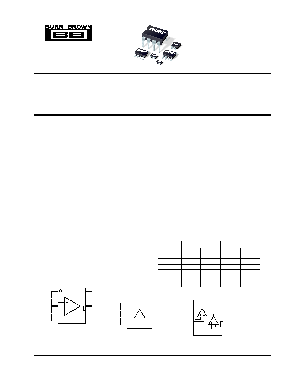
Micro
SIZE PACKAGES:
SOT23-5
SOT23-8
q
SINGLE-SUPPLY OPERATION
q
RAIL-TO-RAIL OUTPUT SWING
q
FET-INPUT: I
B
= 10pA max
q
HIGH SPEED:
OPA337: 3MHz, 1.2V/
µ
s (G = 1)
OPA338: 12.5MHz, 4.6V/
µ
s (G = 5)
q
OPERATION FROM 2.5V to 5.5V
q
HIGH OPEN-LOOP GAIN: 120dB
q
LOW QUIESCENT CURRENT: 525
µ
A/amp
q
SINGLE AND DUAL VERSIONS
DESCRIPTION
The OPA337 and OPA338 series rail-to-rail output CMOS
operational amplifiers are designed for low cost and minia-
ture applications. Packaged in the new SOT23-8, the
OPA2337EA and OPA2338EA are Burr-Brown's smallest
dual op amps. At 1/4 the size of a conventional SO-8 surface
mount, they are ideal for space-sensitive applications.
Utilizing advanced CMOS technology, OPA337 and
OPA338 op amps provide low bias current, high-speed
operation, high open-loop gain, and rail-to-rail output
swing. They operate on a single supply with operation as
low as 2.5V while drawing only 525
µ
A quiescent current.
In addition, the input common-mode voltage range in-
cludes ground--ideal for single-supply operation.
The OPA337 series is unity-gain stable. The OPA338
series is optimized for gains greater than or equal to five.
They are easy to use and free from phase inversion and
overload problems found in some other op amps. Excel-
lent performance is maintained as the amplifiers swing to
their specified limits. The dual versions feature completely
independent circuitry for lowest crosstalk and freedom
from interaction, even when overdriven or overloaded.
Micro
SIZE, Single-Supply
CMOS OPERATIONAL AMPLIFIERS
Micro
Amplifier
TM
Series
APPLICATIONS
q
BATTERY-POWERED INSTRUMENTS
q
PHOTODIODE PRE-AMPS
q
MEDICAL INSTRUMENTS
q
TEST EQUIPMENT
q
AUDIO SYSTEMS
q
DRIVING ADCs
q
CONSUMER PRODUCTS
1
2
3
4
8
7
6
5
V+
Out B
≠In B
+In B
Out A
≠In A
+In A
V≠
OPA2337, OPA2338
8-Pin DIP
(1)
, SO-8, SOT23-8
A
B
1
2
3
4
8
7
6
5
NC
V+
Output
NC
NC
≠In
+In
V≠
OPA337, OPA338
8-Pin DIP
(1)
, SO-8, MSOP-8
(1)
1
2
3
5
4
V+
≠In
Out
V≠
+In
OPA337, OPA338
SOT23-5
NOTE: (1) DIP AND MSOP-8 versions for OPA337, OPA2337 only.
SPICE Model available at www.burr-brown.com
For most current data sheet and other product
information, visit www.burr-brown.com
OPA337
OPA2337
OPA338
OPA2338
G = 1 STABLE
G
5 STABLE
SINGLE
DUAL
SINGLE
DUAL
PACKAGE
OPA337
OPA2337
OPA338
OPA2338
SOT23-5
SOT23-8
MSOP-8
SO-8
DIP-8
OPA337
OPA2337
OPA2338
2
Æ
OPA337, OPA2337
OPA338, OPA2338
SPECIFICATIONS: V
S
= 2.7V to 5.5V
At T
A
= +25
∞
C, and R
L
= 25k
connected to V
S
/2, unless otherwise noted.
Boldface limits apply over the specified temperature range, ≠40
∞
C to +85
∞
C, V
S
= 5V.
The information provided herein is believed to be reliable; however, BURR-BROWN assumes no responsibility for inaccuracies or omissions. BURR-BROWN assumes
no responsibility for the use of this information, and all use of such information shall be entirely at the user's own risk. Prices and specifications are subject to change
without notice. No patent rights or licenses to any of the circuits described herein are implied or granted to any third party. BURR-BROWN does not authorize or warrant
any BURR-BROWN product for use in life support devices and/or systems.
OPA337NA, EA, UA, PA
OPA2337EA, UA, PA
OPA338NA, UA
OPA2338EA, UA
PARAMETER
CONDITION
MIN
TYP
(1)
MAX
UNITS
OFFSET VOLTAGE
Input Offset Voltage
V
OS
±
0.5
±
3
mV
T
A
= ≠40
∞
C to +85
∞
C
±
3.5
mV
vs Temperature
dV
OS
/dT
±
2
µ
V/
∞
C
vs Power Supply Rejection Ratio
PSRR
V
S
= 2.7V to 5.5V
25
125
µ
V/V
T
A
= ≠40
∞
C to +85
∞
C
V
S
= 2.7V to 5.5V
125
µ
V/V
Channel Separation (dual versions)
dc
0.3
µ
V/V
INPUT BIAS CURRENT
Input Bias Current
I
B
±
0.2
±
10
pA
T
A
= ≠40
∞
C to +85
∞
C
See Typical Curve
Input Offset Current
I
OS
±
0.2
±
10
pA
NOISE
Input Voltage Noise, f = 0.1Hz to 10Hz
6
µ
Vp-p
Input Voltage Noise Density, f = 1kHz
e
n
26
nV/
Hz
Current Noise Density, f = 1kHz
i
n
0.6
fA/
Hz
INPUT VOLTAGE RANGE
Common-Mode Voltage Range
V
CM
T
A
= ≠40
∞
C to +85
∞
C
≠0.2
(V+) ≠ 1.2
V
Common-Mode Rejection Ratio
CMRR
≠0.2V < V
CM
< (V+) ≠ 1.2V
74
90
dB
T
A
= ≠40
∞
C to +85
∞
C
≠0.2V < V
CM
< (V+) ≠ 1.2V
74
dB
INPUT IMPEDANCE
Differential
10
13
|| 2
|| pF
Common-Mode
10
13
|| 4
|| pF
OPEN-LOOP GAIN
Open-Loop Voltage Gain
A
OL
R
L
= 25k
, 125mV < V
O
< (V+) ≠ 125mV
100
120
dB
T
A
= ≠40
∞
C to +85
∞
C
R
L
= 25k
, 125mV < V
O
< (V+) ≠ 125mV
100
dB
R
L
= 5k
, 500mV < V
O
< (V+) ≠ 500mV
100
114
dB
T
A
= ≠40
∞
C to +85
∞
C
R
L
= 5k
, 500mV < V
O
< (V+) ≠ 500mV
100
dB
OPA337 FREQUENCY RESPONSE
Gain-Bandwidth Product
GBW
V
S
= 5V, G = 1
3
MHz
Slew Rate
SR
V
S
= 5V, G = 1
1.2
V/
µ
s
Settling Time: 0.1%
V
S
= 5V, 2V Step, C
L
= 100pF, G = 1
2
µ
s
0.01%
V
S
= 5V, 2V Step, C
L
= 100pF, G = 1
2.5
µ
s
Overload Recovery Time
V
IN
∑ G = V
S
2
µ
s
Total Harmonic Distortion + Noise
THD+N
V
S
= 5V, V
O
= 3Vp-p, G = 1, f = 1kHz
0.001
%
OPA338 FREQUENCY RESPONSE
Gain-Bandwidth Product
GBW
V
S
= 5V, G = 5
12.5
MHz
Slew Rate
SR
V
S
= 5V, G = 5
4.6
V/
µ
s
Settling Time: 0.1%
V
S
= 5V, 2V Step, C
L
= 100pF, G = 5
1.4
µ
s
0.01%
V
S
= 5V, 2V Step, C
L
= 100pF, G = 5
1.9
µ
s
Overload Recovery Time
V
IN
∑ G = V
S
0.5
µ
s
Total Harmonic Distortion + Noise
THD+N
V
S
= 5V, V
O
= 3Vp-p, G = 5, f = 1kHz
0.0035
%
OUTPUT
Voltage Output Swing from Rail
(2)
R
L
= 25k
,
A
OL
100dB
40
125
mV
T
A
= ≠40
∞
C to +85
∞
C
R
L
= 25k
,
A
OL
100dB
125
mV
R
L
= 5k
,
A
OL
100dB
150
500
mV
T
A
= ≠40
∞
C to +85
∞
C
R
L
= 5k
,
A
OL
100dB
500
mV
Short-Circuit Current
I
SC
±
9
mA
Capacitive Load Drive
C
LOAD
See Typical Curve
POWER SUPPLY
Specified Voltage Range
V
S
T
A
= ≠40
∞
C to +85
∞
C
2.7
5.5
V
Minimum Operating Voltage
2.5
V
Quiescent Current (per amplifier)
I
Q
I
O
= 0
0.525
1
mA
T
A
= ≠40
∞
C to +85
∞
C
I
O
= 0
1.2
mA
3
Æ
OPA337, OPA2337
OPA338, OPA2338
PACKAGE
SPECIFIED
DRAWING
TEMPERATURE
PACKAGE
ORDERING
TRANSPORT
PRODUCT
DESCRIPTION
PACKAGE
NUMBER
RANGE
MARKING
NUMBER
(1)
MEDIA
OPA337 Series
OPA337NA
Single, G = 1 Stable
5-Lead SOT23-5
331
≠40
∞
C to +85
∞
C
C37
OPA337NA/250
Tape and Reel
"
"
"
"
"
"
OPA337NA/3K
Tape and Reel
OPA337EA
Single, G = 1 Stable
MSOP-8
337
≠40
∞
C to +85
∞
C
G37
OPA337EA/250
Tape and Reel
"
"
"
"
"
"
OPA337EA/2K5
Tape and Reel
OPA337PA
Single, G = 1 Stable
8-Pin DIP
006
≠40
∞
C to +85
∞
C
OPA337PA
OPA337PA
Rails
OPA337UA
Single, G = 1 Stable
SO-8 Surface Mount
182
≠40
∞
C to +85
∞
C
OPA337UA
OPA337UA
Rails
"
"
"
"
"
"
OPA337UA/2K5
Tape and Reel
OPA2337EA
Dual, G = 1 Stable
8-Lead SOT23-8
348
≠40
∞
C to +85
∞
C
A7
OPA2337EA/250
Tape and Reel
"
"
"
"
"
"
OPA2337EA/3K
Tape and Reel
OPA2337PA
Dual, G = 1 Stable
8-Pin DIP
006
≠40
∞
C to +85
∞
C
OPA2337PA
OPA2337PA
Rails
OPA2337UA
Dual, G = 1 Stable
SO-8 Surface Mount
182
≠40
∞
C to +85
∞
C
OPA2337UA
OPA2337UA
Rails
"
"
"
"
"
"
OPA2337UA/2K5
Tape and Reel
OPA338 Series
OPA338NA
Single, G
5 Stable
5-Lead SOT23-5
331
≠40
∞
C to +85
∞
C
A38
OPA338NA/250
Tape and Reel
"
"
"
"
"
"
OPA338NA/3K
Tape and Reel
OPA338UA
Single, G
5 Stable
SO-8 Surface Mount
182
≠40
∞
C to +85
∞
C
OPA338UA
OPA338UA
Rails
"
"
"
"
"
"
OPA338UA/2K5
Tape and Reel
OPA2338EA
Dual, G
5 Stable
8-Lead SOT23-8
348
≠40
∞
C to +85
∞
C
A8
OPA2338EA/250
Tape and Reel
"
"
"
"
"
"
OPA2338EA/3K
Tape and Reel
OPA2338UA
Dual, G
5 Stable
SO-8 Surface Mount
182
≠40
∞
C to +85
∞
C
OPA2338UA
OPA2338UA
Rails
"
"
"
"
"
"
OPA2338UA/2K5
Tape and Reel
NOTES: (1) Models with a slash (/) are available only in Tape and Reel in the quantities indicated (e.g., /2K5 indicates 2500 devices per reel). Ordering 2500 pieces
of "OPA2337UA/2K5" will get a single 2500-piece Tape and Reel.
SPECIFICATIONS: V
S
= 2.7V to 5.5V
(Cont.)
At T
A
= +25
∞
C, and R
L
= 25k
connected to V
S
/2, unless otherwise noted.
Boldface limits apply over the specified temperature range, ≠40
∞
C to +85
∞
C, V
S
= 5V.
OPA337NA, EA, UA, PA
OPA2337EA, UA, PA
OPA338NA, UA
OPA2338EA, UA
PARAMETER
CONDITION
MIN
TYP
MAX
UNITS
TEMPERATURE RANGE
Specified Range
≠40
+85
∞
C
Operating Range
≠55
+125
∞
C
Storage Range
≠55
+125
∞
C
Thermal Resistance
JA
SOT23-5 Surface Mount
200
∞
C/W
SOT23-8 Surface Mount
200
∞
C/W
MSOP-8
150
∞
C/W
SO-8 Surface Mount
150
∞
C/W
8-Pin DIP
100
∞
C/W
NOTES: (1) V
S
= 5V. (2) Output voltage swings are measured between the output and negative and positive power supply rails.
ELECTROSTATIC
DISCHARGE SENSITIVITY
This integrated circuit can be damaged by ESD. Burr-Brown
recommends that all integrated circuits be handled with
appropriate precautions. Failure to observe proper handling
and installation procedures can cause damage.
ESD damage can range from subtle performance degrada-
tion to complete device failure. Precision integrated circuits
may be more susceptible to damage because very small
parametric changes could cause the device not to meet its
published specifications.
Supply Voltage ................................................................................... 5.5V
Input Voltage
(2)
.................................................. (V≠) ≠0.5V to (V+) +0.5V
Input Current
(2)
................................................................................. 10mA
Output Short Circuit
(3)
.............................................................. Continuous
Operating Temperature .................................................. ≠55
∞
C to +125
∞
C
Storage Temperature ..................................................... ≠55
∞
C to +125
∞
C
Junction Temperature ...................................................................... 150
∞
C
Lead Temperature (soldering, 10s) ................................................. 300
∞
C
NOTES: (1) Stresses above these ratings may cause permanent damage.
Exposure to absolute maximum ratings for extended periods may degrade
device reliability. (2) Input signal voltage is limited by internal diodes
connected to power supplies. See text. (3) Short circuit to ground, one
amplifier per package.
ABSOLUTE MAXIMUM RATINGS
(1)
PACKAGE/ORDERING INFORMATION
4
Æ
OPA337, OPA2337
OPA338, OPA2338
TYPICAL PERFORMANCE CURVES
At T
A
= +25
∞
C, V
S
= +5V, and R
L
= 25k
connected to V
S
/2, unless otherwise noted.
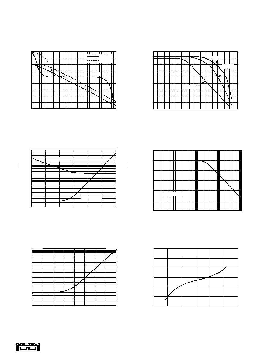
OPEN-LOOP GAIN/PHASE vs FREQUENCY
Frequency (Hz)
Open-Loop Gain (dB)
Phase (
∞
)
160
140
120
100
80
60
40
20
0
≠20
1
10
100
10k
1k
100k
10M
1M
OPA337
OPA338
G
0
≠45
≠90
≠135
≠180
CHANNEL SEPARATION vs FREQUENCY
Frequency (Hz)
Channel Separation (dB)
140
130
120
110
100
90
80
100
10k
1k
1M
100k
Dual Versions
INPUT BIAS CURRENT
vs INPUT COMMON-MODE VOLTAGE
Common-Mode Voltage (V)
Input Bias Current (pA)
0.5
0.4
0.3
0.2
0.1
0
≠0.1
≠1
2
1
0
5
4
3
INPUT BIAS CURRENT vs TEMPERATURE
Temperature (
∞
C)
Input Bias Current (pA)
100
10
1
0.1
0.01
≠75
≠50
≠25
0
25
50
75
100
125
POWER SUPPLY REJECTION RATIO AND
COMMON-MODE REJECTION RATIO vs FREQUENCY
Frequency (Hz)
PSRR, CMRR (dB)
100
90
80
70
60
50
40
30
20
10
1
10
100
1k
10k
100k
1M
10M
+PSRR
≠PSRR
CMRR
INPUT VOLTAGE AND CURRENT NOISE
SPECTRAL DENSITY vs FREQUENCY
Frequency (Hz)
Voltage Noise (nV
Hz)
1k
100
10
1
0.1
1k
100
10
1
0.1
1
10
100
1k
10k
100k
1M
Current Noise (fA
Hz)
Voltage Noise
Current Noise
5
Æ
OPA337, OPA2337
OPA338, OPA2338
TYPICAL PERFORMANCE CURVES
(Cont.)
At T
A
= +25
∞
C, V
S
= +5V, and R
L
= 25k
connected to V
S
/2, unless otherwise noted.
MAXIMUM OUTPUT VOLTAGE vs FREQUENCY
Frequency (Hz)
Output Voltage (Vp-p)
6
5
4
3
2
1
0
10k
100k
100M
1M
10M
Maximum output
voltage without slew
rate-induced distortion.
OPA337
OPA338
TOTAL HARMONIC DISTORTION + NOISE
vs FREQUENCY
Frequency (Hz)
THD+N (%)
0.1
0.01
0.001
0.0001
20
100
1k
10k
20k
G = +10, R
L
= 5k
, 25k
G = +5, R
L
= 5k
, 25k
R
L
= 25k
R
L
= 5k
G = +1
V
O
= 3Vp-p
OPA337
OPA338
A
OL
, CMRR, PSRR vs TEMPERATURE
Temperature (∞C)
A
OL
, CMRR (dB)
PSRR (dB)
140
130
120
110
100
90
80
130
120
110
100
90
80
70
≠75
≠50
≠25
0
25
50
75
100
125
PSRR
CMRR
A
OL
QUIESCENT CURRENT AND SHORT-CIRCUIT CURRENT
vs TEMPERATURE
Temperature (
∞
C)
Quiescent Current (
µ
A)
600
550
500
450
400
350
300
12
11
10
9
8
7
6
Short-Circuit Current (mA)
≠75
≠50
≠25
0
25
50
75
100
125
≠I
SC
+I
SC
I
Q
OUTPUT VOLTAGE SWING vs OUTPUT CURRENT
Output Current (mA)
Output Voltage (V)
2.5
2.0
1.5
1.0
0.5
0
≠0.5
≠1.0
≠1.5
≠2.0
≠2.5
0
±
3
±
2
±
1
±
6
±
7
±
8
±
5
±
4
125
∞
C
Sinking
Sourcing
25
∞
C
V
S
=
±
2.5V
R
L
Tied to Ground
≠55
∞
C
≠55
∞
C
QUIESCENT AND SHORT-CIRCUIT CURRENT
vs SUPPLY VOLTAGE
Supply Voltage (V)
Quiescent Current (
µ
A)
Short-Circuit Current (mA)
700
650
600
550
500
450
400
±
12
±
10
±
8
±
6
±
4
±
2
0
2.5
4.0
3.5
3.0
5.5
5.0
4.5
+I
SC
≠I
SC
I
Q
6
Æ
OPA337, OPA2337
OPA338, OPA2338
TYPICAL PERFORMANCE CURVES
(Cont.)
At T
A
= +25
∞
C, V
S
= +5V, and R
L
= 25k
connected to V
S
/2, unless otherwise noted.
SMALL-SIGNAL STEP RESPONSE
C
L
= 100pF, V
S
= +5V
1
µ
s/div
50mV/div
LARGE-SIGNAL STEP RESPONSE
C
L
= 100pF, V
S
= +5V
2
µ
s/div
500mV/div
OFFSET VOLTAGE DRIFT
PRODUCTION DISTRIBUTION
Percent of Amplifiers (%)
Offset Voltage Drift (µV/∞C)
30
25
20
15
10
5
0
Typical distribution
of packaged units
0
0.5 1.0 1.5 2.0 2.5 3.0 3.5 4.0 4.5 5.0 5.5 6.0
OFFSET VOLTAGE
PRODUCTION DISTRIBUTION
Percent of Amplifiers (%)
Offset Voltage (mV)
≠3.0
≠2.5
≠2.0
≠1.5
≠1.0
≠0.5
0.0
0.5
1.0
1.5
2.0
2.5
3.0
25
20
15
10
5
0
Typical distribution
of packaged units.
OPA337
G = 1
OPA338
G = 5
OPA337
G = 1
OPA338
G = 5
SETTLING TIME vs CLOSED-LOOP GAIN
Closed-Loop Gain (V/V)
Settling Time (
µ
s)
100
10
1
1
1k
10
100
0.01%
OPA337
0.1%
OPA338
SMALL-SIGNAL OVERSHOOT vs LOAD CAPACITANCE
Load Capacitance (pF)
Overshoot (%)
60
50
40
30
20
10
0
10
10k
100
1k
OPA337
(G =
±
1)
OPA337
(G =
±
10)
OPA338
(G =
±
50)
OPA338
(G =
±
5)
7
Æ
OPA337, OPA2337
OPA338, OPA2338
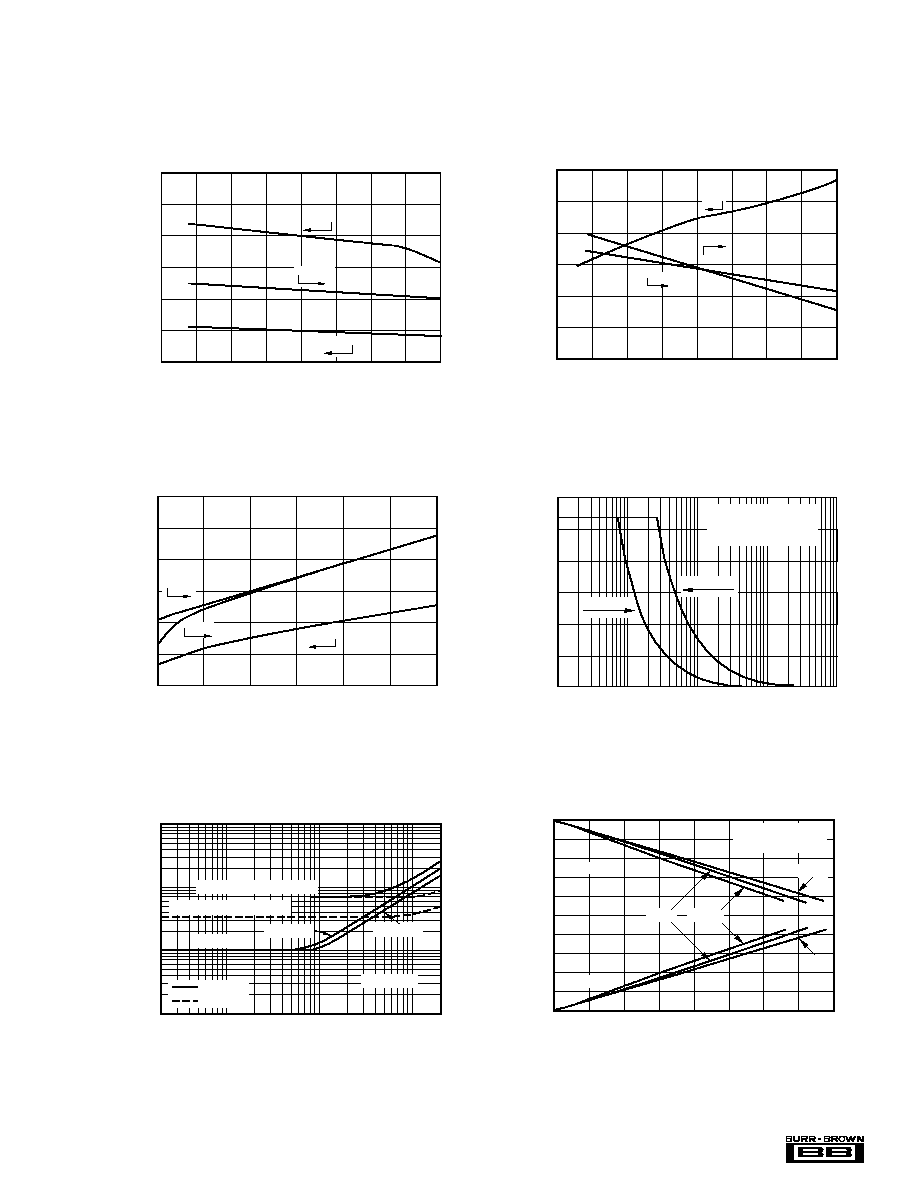
APPLICATIONS INFORMATION
The OPA337 series and OPA338 series are fabricated on a
state-of-the-art CMOS process. The OPA337 series is unity-
gain stable. The OPA338 series is optimized for gains
greater than or equal to five. Both are suitable for a wide
range of general purpose applications. Power supply pins
should be bypassed with 0.01
µ
F ceramic capacitors.
OPERATING VOLTAGE
The OPA337 series and OPA338 series can operate from a
+2.5V to +5.5V single supply with excellent performance.
Unlike most op amps which are specified at only one supply
voltage, these op amps are specified for real-world applica-
tions; a single limit applies throughout the +2.7V to +5.5V
supply range. This allows a designer to have the same
assured performance at any supply voltage within the speci-
fied voltage range. Most behavior remains unchanged
throughout the full operating voltage range. Parameters
which vary significantly with operating voltage are shown in
typical performance curves.
FIGURE 2. Input Current Protection for Voltages Exceeding
the Supply Voltage.
5k
OPA337
10mA max
+5V
V
IN
V
OUT
I
OVERLOAD
0
3V
V
OUT
, G = +1
(limited by input
common-mode
range)
≠3V
V
OUT
, G = ≠1
(not limited by
input common-
mode range.)
G =
±
1
OPA337, V
IN
=
±
3V Greater Than V
S
=
±
2.5V
FIGURE 1. OPA337--No Phase Inversion with Inputs
Greater than the Power Supply Voltage.
INPUT VOLTAGE
The input common-mode range extends from (V≠) ≠ 0.2V to
(V+) ≠ 1.2V. For normal operation, inputs should be
limited to this range. The absolute maximum input voltage
is 500mV beyond the supplies. Inputs greater than the
input common-mode range but less than maximum input
voltage, while not valid, will not cause any damage to the
op amp. Furthermore, if input current is limited the inputs
may go beyond the power supplies without phase inver-
sion (Figure 1) unlike some other op amps.
Normally, input currents are 0.2pA. However, large inputs
(greater than 500mV beyond the supply rails) can cause
excessive current to flow in or out of the input pins.
Therefore, as well as keeping the input voltage below the
maximum rating, it is also important to limit the input
current to less than 10mA. This is easily accomplished
with an input resistor as shown in Figure 2.
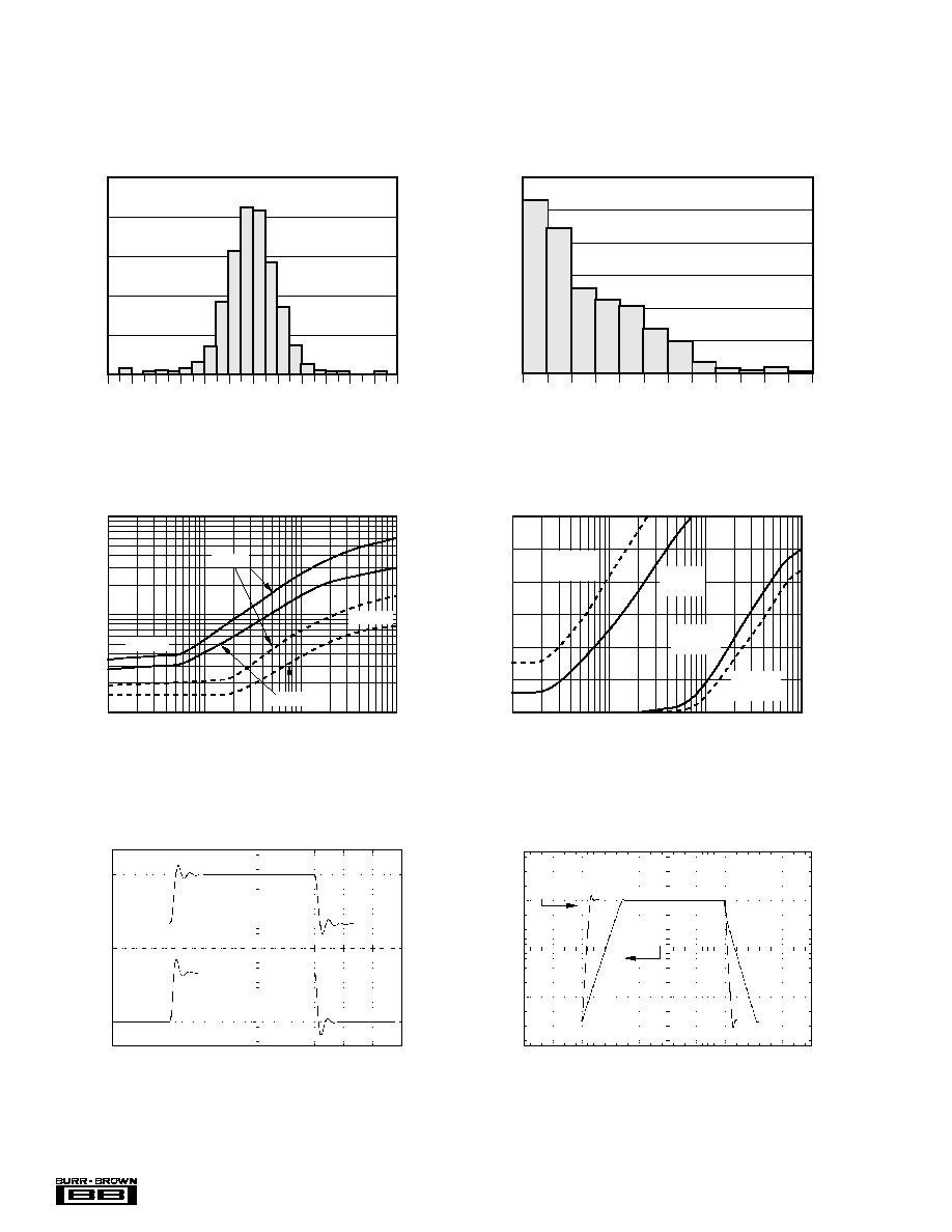
USING THE OPA338 IN LOW GAINS
The OPA338 series is optimized for gains greater than or
equal to five. It has significantly wider bandwidth (12.5MHz)
and faster slew rate (4.6V/
µ
s) when compared to the OPA337
series. The OPA338 series can be used in lower gain con-
figurations at low frequencies while maintaining its high
slew rate with the proper compensation.
Figure 3 shows the OPA338 in a unity-gain buffer configu-
ration. At dc, the compensation capacitor C
1
is effectively
"open" resulting in 100% feedback (closed-loop gain = 1).
As frequency increases, C
1
becomes lower impedance and
closed-loop gain increases, eventually becoming 1 + R
2
/R
1
(in this case five, which is equal to the minimum gain
required for stability).
The required compensation capacitor value can be deter-
mined from the following equation:
C
1
= 1/(2
f
C
R
1
)
Since f
C
may shift with process variations, it is recom-
mended that a value less than f
C
be used for determining C
1
.
With f
C
= 1MHz and R
1
= 2.5k
, the compensation capaci-
tor is about 68pF.
The selection of the compensation capacitor C
1
is important.
A proper value ensures that the closed-loop circuit gain is
greater than or equal to five at high frequencies. Referring to
the "Open-Loop Gain vs Frequency" plot in the Typical
Performance Curves section, the OPA338 gain line (dashed
in the curve) has a constant slope (≠20dB/decade) up to
approximately 3MHz. This frequency is referred to as f
C
.
Beyond f
C
the slope of the curve increases, suggesting that
closed-loop gains less than 5 are not appropriate.
FIGURE 3. Compensation of OPA338 for Unity-Gain Buffer.
C
1
=
1
2
f
C
R
1
R
1
2.5k
C
1
68pF
R
2
10k
OPA338
V
IN
V
OUT
Where f
C
is the frequency at which closed-loop
gains less than five are not appropriate--see text.
Improved slew rate (4.6V/
µ
s) versus
OPA337 (1.2V/
µ
s) in unity gain.
8
Æ
OPA337, OPA2337
OPA338, OPA2338
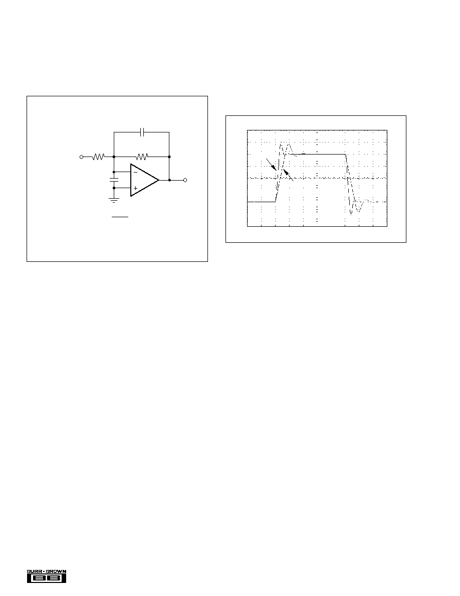
Figure 4 shows a compensation technique using an inverting
configuration. The low frequency gain is set by the resistor
ratio while the high frequency gain is set by the capacitor
ratio. As with the noninverting circuit, for frequencies above
f
C
the gain must be greater than the recommended minimum
stable gain for the op amp.
The capacitor values shown are the nearest standard values.
Capacitor values may need to be adjusted slightly to opti-
mize performance. For more detailed information, consult
the OPA686 product data sheet.
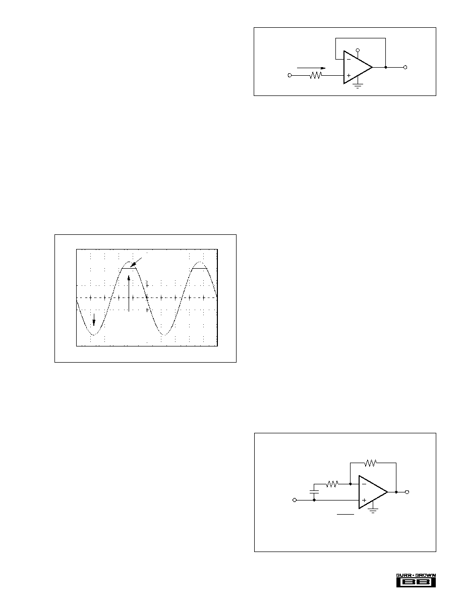
Figure 5 shows the large-signal transient response using the
circuit given in Figure 4. As shown, the OPA338 is stable in
low gain applications and provides improved slew rate
performance when compared to the OPA337.
FIGURE 4. Inverting Compensation Circuit of OPA338 for
Low Gain.
500mV/div
OPA338
2
µ
s/div
FIGURE 5. G = 2, Slew-Rate Comparison of OPA338 and
OPA337.
OPA337
Resistors R
1
and R
2
are chosen to set the desired dc signal
gain. Then the value for C
2
is determined as follows:
C
2
= 1/(2
f
C
R
2
)
C
1
is determined from the desired high frequency gain (G
H
):
C
1
= (G
H
≠ 1) ∑ C
2
For a desired dc gain of 2 and high frequency gain of 10, the
following resistor and capacitor values result:
R
1
= 10k
C
1
= 150pF
R
2
= 5k
C
2
= 15pF
TYPICAL APPLICATION
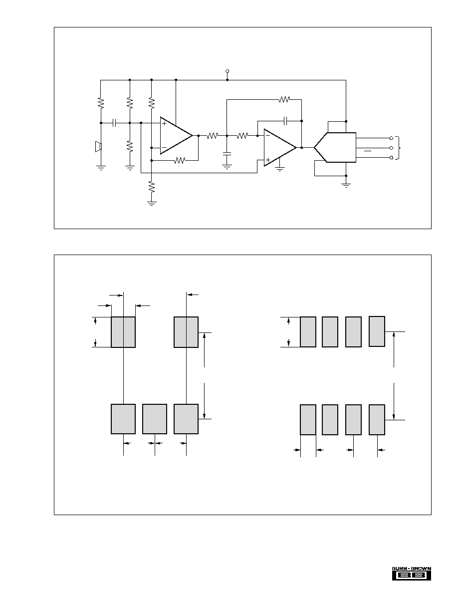
Figure 6 shows the OPA2337 in a typical application. The
ADS7822 is a 12-bit, micro-power sampling analog-to-
digital converter available in the tiny MSOP-8 package. As
with the OPA2337, it operates with a supply voltage as
low as +2.7V. When used with the miniature SOT23-8
package of the OPA2337, the circuit is ideal for space-
limited and low power applications. In addition, OPA2337's
high input impedance allows large value resistors to be
used which results in small physical capacitors, further
reducing circuit size. For further information, consult the
ADS7822 product data sheet.
C
2
= , C
1
= (G
H
≠1) ∑ C
2
1
2
f
C
R
2
C
1
150pF
OPA338
V
IN
V
OUT
R
1
5k
R
2
10k
Where G
H
is the high frequency gain,
G
H
= 1 + C
1
/C
2
Improved slew rate versus OPA337
(see Figure 5).
C
2
15pF
9
Æ
OPA337, OPA2337
OPA338, OPA2338
FIGURE 6. Low Power, Single-Supply, Speech Bandpass Filtered Data Acquisition System.
1/2
OPA2337E
1/2
OPA2337E
ADS7822
12-Bit A/D
C
3
V
+
GND
3
1
8
4
5
6
7
≠IN
+IN
2
C
2
33pF
DCLOCK
Serial
Interface
1000pF
R
1
1.5k
R
4
20k
R
5
20k
R
6
100k
R
8
150k
R
9
510k
R
7
51k
D
OUT
V
REF
V+
= +2.7V to 5V
CS/SHDN
C
1
1000pF
Electret
Microphone
(1)
G = 100
Passband 300Hz to 3kHz
R
3
1M
R
2
1M
NOTE: (1) Electret microphone
with internal transistor (FET)
powered by R
1
.
FIGURE 7. Recommended SOT23-5 and SOT23-8 Solder Footprints.
0.035
(0.889)
0.10
(2.54)
0.018
(0.457)
0.026
(0.66)
SOT23-8
(Package Drawing #348)
Refer to end of data sheet or Appendix C of Burr-Brown IC Data Book for
tolerances and detailed package drawing. For further information on solder
pads for surface-mount packages, consult Application Bulletin AB-132.
SOT23-5
(Package Drawing #331)
0.035
(0.889)
0.10
(2.54)
0.0375
(0.9525)
0.0375
(0.9525)
0.075
(1.905)
0.027
(0.686)