 | –≠–ª–µ–∫—Ç—Ä–æ–Ω–Ω—ã–π –∫–æ–º–ø–æ–Ω–µ–Ω—Ç: OPA604AP | –°–∫–∞—á–∞—Ç—å:  PDF PDF  ZIP ZIP |

FEATURES
q
LOW DISTORTION: 0.0003% at 1kHz
q
LOW NOISE: 10nV/
Hz
q
HIGH SLEW RATE: 25V/
µ
s
q
WIDE GAIN-BANDWIDTH: 20MHz
q
UNITY-GAIN STABLE
q
WIDE SUPPLY RANGE: V
S
=
±
4.5 to
±
24V
q
DRIVES 600
LOAD
q
DUAL VERSION AVAILABLE (OPA2604)
FET-Input, Low Distortion
OPERATIONAL AMPLIFIER
APPLICATIONS
q
PROFESSIONAL AUDIO EQUIPMENT
q
PCM DAC I/V CONVERTER
q
SPECTRAL ANALYSIS EQUIPMENT
q
ACTIVE FILTERS
q
TRANSDUCER AMPLIFIER
q
DATA ACQUISITION
OPA604
DESCRIPTION
The OPA604 is a FET-input operational amplifier
designed for enhanced AC performance. Very low
distortion, low noise and wide bandwidth provide
superior performance in high quality audio and other
applications requiring excellent dynamic performance.
New circuit techniques and special laser trimming of
dynamic circuit performance yield very low harmonic
distortion. The result is an op amp with exceptional
sound quality. The low-noise FET input of the OPA604
provides wide dynamic range, even with high source
impedance. Offset voltage is laser-trimmed to mini-
mize the need for interstage coupling capacitors.
The OPA604 is available in 8-pin plastic mini-DIP
and SO-8 surface-mount packages, specified for the
≠25
∞
C to +85
∞
C temperature range.
Distortion
Rejection
Circuitry
(1)
(3)
(+)
(2)
(≠)
(7)
V+
(6)
V
O
(4)
V≠
Output
Stage
(1)
NOTE: (1) Patents Granted: #5053718, 5019789
(5)
(1)
FPO
© 1992 Burr-Brown Corporation
PDS-1161C
Printed in U.S.A. May, 1995
Æ
International Airport Industrial Park ∑ Mailing Address: PO Box 11400 ∑ Tucson, AZ 85734 ∑ Street Address: 6730 S. Tucson Blvd. ∑ Tucson, AZ 85706
Tel: (520) 746-1111 ∑ Twx: 910-952-1111 ∑ Cable: BBRCORP ∑ Telex: 066-6491 ∑ FAX: (520) 889-1510 ∑ Immediate Product Info: (800) 548-6132
2
Æ
OPA604
The information provided herein is believed to be reliable; however, BURR-BROWN assumes no responsibility for inaccuracies or omissions. BURR-BROWN assumes
no responsibility for the use of this information, and all use of such information shall be entirely at the user's own risk. Prices and specifications are subject to change
without notice. No patent rights or licenses to any of the circuits described herein are implied or granted to any third party. BURR-BROWN does not authorize or warrant
any BURR-BROWN product for use in life support devices and/or systems.
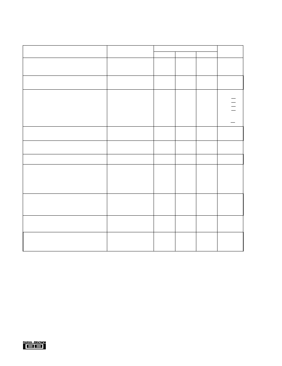
SPECIFICATIONS
ELECTRICAL
T
A
= +25
∞
C, V
S
=
±
15V unless otherwise noted.
OPA604AP, AU
PARAMETER
CONDITION
MIN
TYP
MAX
UNITS
OFFSET VOLTAGE
Input Offset Voltage
±
1
±
5
mV
Average Drift
±
8
µ
V/
∞
C
Power Supply Rejection
V
S
=
±
5 to
±
24V
80
100
dB
INPUT BIAS CURRENT
(1)
Input Bias Current
V
CM
= 0V
50
pA
Input Offset Current
V
CM
= 0V
±
3
pA
NOISE
Input Voltage Noise
Noise Density: f = 10Hz
25
nV/
Hz
f = 100Hz
15
nV/
Hz
f = 1kHz
11
nV/
Hz
f = 10kHz
10
nV/
Hz
Voltage Noise, BW = 20Hz to 20kHz
1.5
µ
Vp-p
Input Bias Current Noise
Current Noise Density, f = 0.1Hz to 20kHz
4
fA/
Hz
INPUT VOLTAGE RANGE
Common-Mode Input Range
±
12
±
13
V
Common-Mode Rejection
V
CM
=
±
12V
80
100
dB
INPUT IMPEDANCE
Differential
10
12
|| 8
|| pF
Common-Mode
10
12
|| 10
|| pF
OPEN-LOOP GAIN
Open-Loop Voltage Gain
V
O
=
±
10V, R
L
= 1k
80
100
dB
FREQUENCY RESPONSE
Gain-Bandwidth Product
G = 100
20
MHz
Slew Rate
20Vp-p, R
L
= 1k
15
25
V/
µ
s
Settling Time: 0.01%
G = ≠1, 10V Step
1.5
µ
s
0.1%
1
µ
s
Total Harmonic Distortion + Noise (THD+N)
G = 1, f = 1kHz
0.0003
%
V
O
= 3.5Vrms, R
L
= 1k
OUTPUT
Voltage Output
R
L
= 600
±
11
±
12
V
Current Output
V
O
=
±
12V
±
35
mA
Short Circuit Current
±
40
mA
Output Resistance, Open-Loop
25
POWER SUPPLY
Specified Operating Voltage
±
15
V
Operating Voltage Range
±
4.5
±
24
V
Current
±
5.3
±
6
mA
TEMPERATURE RANGE
Specification
≠25
+85
∞
C
Storage
≠40
+125
∞
C
Thermal Resistance
(2)
,
JA
90
∞
C/W
NOTES: (1) Typical performance, measured fully warmed-up. (2) Soldered to circuit board--see text.
3
Æ
OPA604
ABSOLUTE MAXIMUM RATINGS
Power Supply Voltage ........................................................................
±
25V
Input Voltage ............................................................... (V≠)≠1V to (V+)+1V
Output Short Circuit to Ground ................................................ Continuous
Operating Temperature ................................................... ≠40
∞
C to +100
∞
C
Storage Temperature ...................................................... ≠40
∞
C to +125
∞
C
Junction Temperature .................................................................... +150
∞
C
Lead Temperature (soldering, 10s) AP .......................................... +300
∞
C
Lead Temperature (soldering, 3s) AU ............................................ +260
∞
C
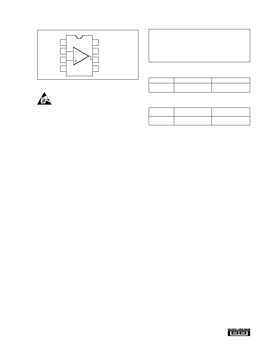
PIN CONFIGURATION
Top View
DIP, SOIC
1
2
3
4
Offset Trim
≠In
+In
≠V
S
8
7
6
5
No Internal Connection
+V
S
Output
Offset Trim
ELECTROSTATIC
DISCHARGE SENSITIVITY
Any integrated circuit can be damaged by ESD. Burr-Brown
recommends that all integrated circuits be handled with ap-
propriate precautions. Failure to observe proper handling and
installation procedures can cause damage.
ESD damage can range from subtle performance degradation
to complete device failure. Precision integrated circuits may
be more susceptible to damage because very small parametric
changes could cause the device not to meet published speci-
fications.
ORDERING INFORMATION
MODEL
PACKAGE
TEMP. RANGE
OPA604AP
8-Pin Plastic DIP
≠25
∞
C to +85
∞
C
OPA604AU
SO-8 Surface-Mount
≠25
∞
C to +85
∞
C
PACKAGE INFORMATION
PACKAGE DRAWING
MODEL
PACKAGE
NUMBER
(1)
OPA604AP
8-Pin Plastic DIP
006
OPA604AU
SO-8 Surface-Mount
182
NOTE: (1) For detailed drawing and dimension table, please see end of data
sheet, or Appendix D of Burr-Brown IC Data Book.
4
Æ
OPA604
TYPICAL PERFORMANCE CURVES
T
A
= +25
∞
C, V
S
=
±
15V unless otherwise noted.
TOTAL HARMONIC DISTORTION + NOISE
vs FREQUENCY
Frequency (Hz)
THD + N (%)
1
0.1
0.01
0.001
0.0001
20
100
1k
10k
20k
G = 100V/V
G = 10V/V
G = 1V/V
Measurement BW = 80kHz
See "Distortion Measure-
ments" for description of
test method.
1k
V =
3.5Vrms
O
TOTAL HARMONIC DISTORTION + NOISE
vs OUTPUT VOLTAGE
Output Voltage (Vp-p)
THD + N (%)
0.1
1
10
100
0.1
0.01
0.001
0.0001
1k
V
O
f = 1kHz
Measurement BW = 80kHz
See "Distortion Measurements"
for description of test method.
OPEN-LOOP GAIN/PHASE vs FREQUENCY
Frequency (Hz)
Voltage Gain (dB)
120
100
80
60
40
20
0
≠20
1
10
100
1k
10k
100k
1M
10M
0
≠45
≠90
≠135
≠180
Phase Shift (Degrees)
G
INPUT VOLTAGE AND CURRENT NOISE
SPECTRAL DENSITY vs FREQUENCY
Frequency (Hz)
Voltage Noise (nV/ Hz)
1
1k
100
10
1
10
100
1k
10k
100k
1M
Current Noise (fA/ Hz)
1k
100
10
1
Voltage Noise
Current Noise
INPUT BIAS AND INPUT OFFSET CURRENT
vs TEMPERATURE
Ambient Temperature (∞C)
Input Bias Current (pA)
≠75
100nA
10nA
1nA
100
10
1
Input Offset Current (pA)
10nA
1nA
100
10
1
0.1
≠50
≠25
0
25
50
75
100
125
Input
Offset Current
Input
Bias Current
INPUT BIAS AND INPUT OFFSET CURRENT
vs INPUT COMMON-MODE VOLTAGE
Common-Mode Voltage (V)
Input Bias Current (pA)
≠15
10nA
1nA
100
10
Input Offset Current (pA)
1nA
100
10
1
≠10
≠5
0
5
10
15
Input
Offset Current
Input
Bias Current
5
Æ
OPA604
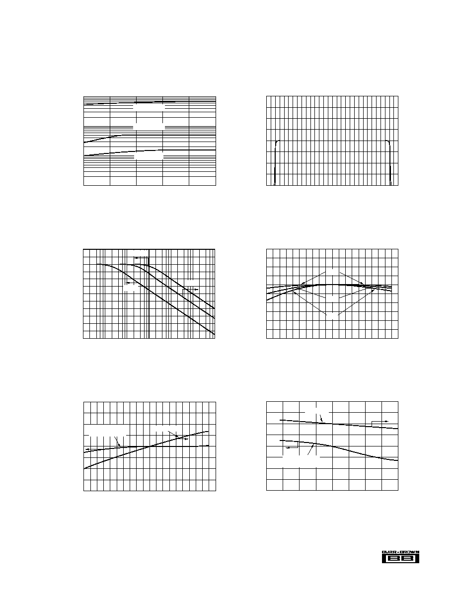
TYPICAL PERFORMANCE CURVES
(CONT)
T
A
= +25
∞
C, V
S
=
±
15V unless otherwise noted.
COMMON-MODE REJECTION
vs COMMON-MODE VOLTAGE
Common-Mode Voltage (V)
Common-Mode Rejection (dB)
≠15
120
110
100
90
80
≠10
≠5
0
5
10
15
POWER SUPPLY AND COMMON-MODE
REJECTION vs FREQUENCY
Frequency (Hz)
Power Supply Rejection (dB)
10
120
100
80
60
40
20
0
100
1k
10k
100k
1M
10M
Common-Mode Rejection (dB)
120
100
80
60
40
20
0
+PSR
≠PSR
CMR
A
OL
, PSR, AND CMR vs SUPPLY VOLTAGE
Supply Voltage (±V
S
)
A
OL
, PSR, CMR (dB)
5
120
110
100
90
80
70
10
15
20
25
CMR
A
OL
PSR
GAIN-BANDWIDTH AND SLEW RATE
vs TEMPERATURE
Temperature (∞C)
Gain-Bandwidth (MHz)
≠75
28
24
20
16
12
≠25
25
75
125
Slew Rate (V/µs)
30
25
20
15
10
≠50
0
50
100
Slew Rate
Gain-Bandwidth
G = +100
INPUT BIAS CURRENT
vs TIME FROM POWER TURN-ON
Time After Power Turn-On (min)
Input Bias Current (pA)
0
1nA
100
10
1
1
2
3
4
5
V
S
= ±24VDC
V
S
= ±15VDC
V
S
= ±5VDC
GAIN-BANDWIDTH AND SLEW RATE
vs SUPPLY VOLTAGE
Supply Voltage (±V
S
)
Gain-Bandwidth (MHz)
5
28
24
20
16
12
10
15
20
25
Slew Rate
Gain-Bandwidth
G = +100
Slew Rate (V/µs)
33
29
25
21
17
6
Æ
OPA604
SMALL-SIGNAL TRANSIENT RESPONSE
Time (µs)
Output Voltage (mV)
TYPICAL PERFORMANCE CURVES
(CONT)
T
A
= +25
∞
C, V
S
=
±
15V unless otherwise noted.
LARGE-SIGNAL TRANSIENT RESPONSE
Time (µs)
Output Voltage (V)
FPO
Bleed to edge
0 1
µ
s 2
µ
s
0 5 10
SETTLING TIME vs CLOSED-LOOP GAIN
Closed-Loop Gain (V/V)
Settling Time (µs)
≠1
5
4
3
2
1
0
≠10
≠100
≠1000
0.01%
0.1%
V
O
= 10V Step
R
L
= 1k
C
L
= 50pF
MAXIMUM OUTPUT VOLTAGE SWING vs FREQUENCY
Frequency (Hz)
Output Voltage (Vp-p)
10k
30
20
10
0
100k
1M
10M
V = ±15V
S
SUPPLY CURRENT vs TEMPERATURE
Ambient Temperature (∞C)
Supply Current (mA)
≠75
7
6
5
4
3
≠50
≠25
0
25
50
75
100
125
V
S
= ±24VDC
V
S
= ±15VDC
V
S
= ±5VDC
SHORT-CIRCUIT CURRENT vs TEMPERATURE
Ambient Temperature (∞C)
Short-Circuit Current (mA)
≠75
60
50
40
30
20
≠50
≠25
0
25
50
75
100
125
I
SC+
and I
SC≠
≠100
+100
≠10
+10

7
Æ
OPA604
TYPICAL PERFORMANCE CURVES
(CONT)
T
A
= +25
∞
C, V
S
=
±
15V unless otherwise noted.
APPLICATIONS INFORMATION
OFFSET VOLTAGE ADJUSTMENT
The OPA604 offset voltage is laser-trimmed and will require
no further trim for most applications. As with most amplifi-
ers, externally trimming the remaining offset can change
drift performance by about 0.3
µ
V/
∞
C for each 100
µ
V of
adjusted offset. The OPA604 can replace many other ampli-
fiers by leaving the external null circuit unconnected.
The OPA604 is unity-gain stable, making it easy to use in a
wide range of circuitry. Applications with noisy or high
impedance power supply lines may require decoupling ca-
pacitors close to the device pins. In most cases, a 1
µ
F
tantalum capacitor at each power supply pin is adequate.
DISTORTION MEASUREMENTS
The distortion produced by the OPA604 is below the mea-
surement limit of virtually all commercially available equip-
ment. A special test circuit, however, can be used to extend
the measurement capabilities.
Op amp distortion can be considered an internal error source
which can be referred to the input. Figure 2 shows a circuit
which causes the op amp distortion to be 101 times greater
than normally produced by the op amp. The addition of R
3
to the otherwise standard noninverting amplifier configura-
tion alters the feedback factor or noise gain of the circuit.
The closed-loop gain is unchanged, but the feedback avail-
able for error correction is reduced by a factor of 101. This
extends the measurement limit, including the effects of the
signal-source purity, by a factor of 101. Note that the input
signal and load applied to the op amp are the same as with
conventional feedback without R
3
.
Validity of this technique can be verified by duplicating
measurements at high gain and/or high frequency where the
distortion is within the measurement capability of the test
equipment. Measurements for this data sheet were made
with the Audio Precision System One which greatly simpli-
fies such repetitive measurements. The measurement tech-
nique can, however, be performed with manual distortion
measurement instruments.
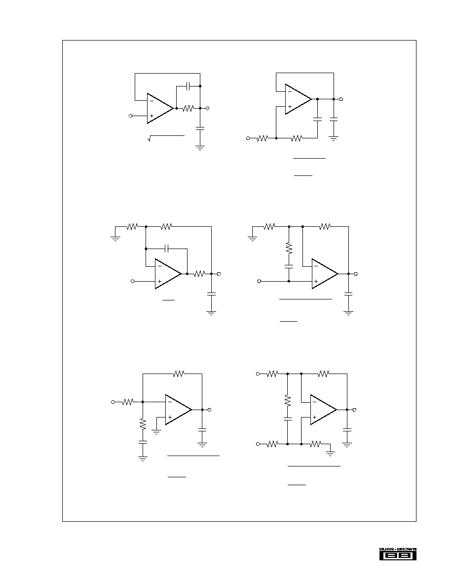
CAPACITIVE LOADS
The dynamic characteristics of the OPA604 have been
optimized for commonly encountered gains, loads and oper-
ating conditions. The combination of low closed-loop gain
and capacitive load will decrease the phase margin and may
lead to gain peaking or oscillations. Load capacitance reacts
with the op amp's open-loop output resistance to form an
additional pole in the feedback loop. Figure 3 shows various
circuits which preserve phase margin with capacitive load.
Request Application Bulletin AB-028 for details of analysis
techniques and applications circuits.
For the unity-gain buffer, Figure 3a, stability is preserved by
adding a phase-lead network, R
C
and C
C
. Voltage drop
FIGURE 1. Offset Voltage Trim.
Supply Voltage, ±V
S
(V)
6
8
10
12
14
16
18
20
22
24
0.5
0.45
0.40
0.35
0.30
0.25
0.20
0.15
0.10
0.05
Power Dissipation (W)
POWER DISSIPATION vs SUPPLY VOLTAGE
No signal
or no load
Typical high-level
music R
L
= 600
Worst case sine
wave R
L
= 600
Ambient Temperature (∞C)
0
1.4
1.2
1.0
0.8
0.6
0.4
0.2
0
Total Power Dissipation (W)
MAXIMUM POWER DISSIPATION vs TEMPERATURE
25
50
75
100
125
150
J-A
= 90∞C/W
Soldered to
Circuit Board
(see text)
Maximum
Specified Operating
Temperature
85∞C
OPA604
±50mV Typical
Trim Range
NOTE: (1) 50k
to 1M
Trim Potentiometer
(100k
Recommended)
+V
CC
≠V
CC
7
6
5
1
(1)
4
3
2

8
Æ
OPA604
across R
C
will reduce output voltage swing with heavy
loads. An alternate circuit, Figure 3b, does not limit the
output with low load impedance. It provides a small amount
of positive feedback to reduce the net feedback factor. Input
impedance of this circuit falls at high frequency as op amp
gain rolloff reduces the bootstrap action on the compensa-
tion network.
Figures 3c and 3d show compensation techniques for
noninverting amplifiers. Like the follower circuits, the cir-
cuit in Figure 3d eliminates voltage drop due to load current,
but at the penalty of somewhat reduced input impedance at
high frequency.
Figures 3e and 3f show input lead compensation networks
for inverting and difference amplifier configurations.
NOISE PERFORMANCE
Op amp noise is described by two parameters--noise volt-
age and noise current. The voltage noise determines the
noise performance with low source impedance. Low noise
bipolar-input op amps such as the OPA27 and OPA37
provide very low voltage noise. But if source impedance is
greater than a few thousand ohms, the current noise of
bipolar-input op amps react with the source impedance and
will dominate. At a few thousand ohms source impedance
and above, the OPA604 will generally provide lower noise.
POWER DISSIPATION
The OPA604 is capable of driving a 600
load with power
supply voltages up to
±
24V. Internal power dissipation is
increased when operating at high power supply voltage. The
typical performance curve, Power Dissipation vs Power
Supply Voltage, shows quiescent dissipation (no signal or
no load) as well as dissipation with a worst case continuous
sine wave. Continuous high-level music signals typically
produce dissipation significantly less than worst case sine
waves.
Copper leadframe construction used in the OPA604 im-
proves heat dissipation compared to conventional plastic
packages. To achieve best heat dissipation, solder the device
directly to the circuit board and use wide circuit board
traces.
OUTPUT CURRENT LIMIT
Output current is limited by internal circuitry to approxi-
mately
±
40mA at 25
∞
C. The limit current decreases with
increasing temperature as shown in the typical curves.
FIGURE 2. Distortion Test Circuit.
R
2
OPA604
R
1
R
3
V
O
= 10Vp-p
(3.5Vrms)
Generator
Output
Analyzer
Input
Audio Precision
System One
Analyzer
(1)
R
L
1k
IBM PC
or
Compatible
SIG.
GAIN
DIST.
GAIN
R
1
R
2
R
3
500
50
5k
5k
5k
50
500
1
10
100
101
101
101
NOTE: (1) Measurement BW = 80kHz
9
Æ
OPA604
FIGURE 3. Driving Large Capacitive Loads.
NOTE: Design equations and component values are approximate. User adjustment is required for optimum performance.
C
C
820pF
R
C
750
C
L
5000pF
e
i
C
C
=
120 X 10
≠12
C
L
(a)
e
o
C
L
5000pF
e
i
R
C
=
(b)
R
C
10
C
C
0.47µF
R
2
2k
R
2
4C
L
X 10
10
≠ 1
C
C
=
C
L
X 10
3
R
C
e
o
C
L
5000pF
R
2
10k
R
1
10k
C
C
=
50
R
2
C
L
e
i
R
C
25
C
C
24pF
(c)
e
o
C
L
5000pF
R
2
2k
R
1
2k
e
i
R
C
20
C
C
0.22µF
(d)
R
C
=
R
2
2C
L
X 10
10
≠ (1 + R
2
/R
1
)
e
o
C
L
5000pF
R
2
2k
R
1
2k
e
i
R
C
20
C
C
0.22µF
(e)
R
C
=
R
2
2C
L
X 10
10
≠ (1 + R
2
/R
1
)
e
o
C
L
5000pF
R
2
2k
R
1
2k
e
1
R
C
20
C
C
0.22µF
(f)
R
C
=
R
2
2C
L
X 10
10
≠ (1 + R
2
/R
1
)
R
3
2k
e
2
R
4
2k
e
o
OPA604
C
C
=
C
L
X 10
3
R
C
C
C
=
C
L
X 10
3
R
C
C
C
=
C
L
X 10
3
R
C
OPA604
OPA604
OPA604
OPA604
OPA604
10
Æ
OPA604
FIGURE 5. Three-Pole Generalized Immittance Converter (GIC) Low-Pass Filter.
FIGURE 4. Three-Pole Low-Pass Filter.
R
5
2k
V
O
C
3
1000pF
Low-pass
3-pole Butterworth
f
≠3dB
= 40kHz
R
1
6.04k
V
IN
R
2
4.02k
R
2
4.02k
C
2
1000pF
C
1
1000pF
R
4
5.36k
See Application Bulletin AB-026
for information on GIC filters.
1
2
OPA2604
1
2
OPA2604
OPA604
FIGURE 6. Differential Amplifier with Low-Pass Filter.
R
4
22k
R
3
10k
V
O
C
2
2000pF
R
2
22k
C
1
3000pF
R
1
2.7k
V
IN
f
p
= 20kHz
C
3
100pF
OPA604
V
O
G = 1
100pF
≠
V
IN
+
7.87k
7.87k
10k
10k
10k
10k
100kHz Input Filter
OPA604
1
2
OPA2604
1
2
OPA2604

11
Æ
OPA604
FIGURE 8. Digital Audio DAC I-V Amplifier.
FIGURE 7. High Impedance Amplifier.
FIGURE 9. Using Two OPA604 Op Amps to Double the Output Current to a Load.
OPA604
OPA604
A
1
A
2
V
IN
R
1
R
2
I
1
R
4
51
I
2
OPA604
R
3
51
I
L
= I
1
+ I
2
Load
V
OUT
= V
IN
(1+R
2
/R
1
)
V
OUT
OPA604
G = 101
(40dB)
100
10k
Piezoelectric
Transducer
1M
(1)
NOTE: (1) Provides input
bias current return path.
OPA604
V
O
= ±3Vp
R
F
= Internal feedback resistance = 1.5k
f
C
= Crossover frequency = 8MHz
C
1
(1)
NOTE: (1) C
1
C
OUT
2
R
f
f
c
To low-pass
filter.
OPA604
5
6
9
PCM63
20-bit
D/A
Converter
10

12
Æ
OPA604
1
0
0
1
I
C
(mA)
0
5
log
(V
O
)
1
2
3
4
f
O
2f
O
3f
O
4f
O
5f
O
V
BE
= 1kHz + DC Bias
V
BE
(V)
0.65
FFT
Frequency (kHz)
1
0
1
0
≠I
D
(mA)
0
5
log
(V
O
)
1
2
3
4
f
O
2f
O
3f
O
4f
O
5f
O
V
GS
= 1kHz + DC Bias
V
GS
(V)
FFT
Frequency (kHz)
V
O
I
D
V
GS
V
O
I
C
V
BE
FIGURE 10. I-V and Spectral Response of NPN and
JFET.
THE OPA604 DESIGN
The OPA604 uses FETs throughout the signal path,
including the input stage, input-stage load, and the
important phase-splitting section of the output stage.
Bipolar transistors are used where their attributes,
such as current capability are important, and where
their transfer characteristics have minimal impact.
The topology consists of a single folded-cascode gain
stage followed by a unity-gain output stage. Differen-
tial input transistors J
1
and J
2
are special large-geom-
etry, P-channel JFETs. Input stage current is a rela-
tively high 800
µ
A, providing high transconductance
and reducing voltage noise. Laser trimming of stage
currents and careful attention to symmetry yields a
nearly symmetrical slew rate of
±
25V/
µ
s.
The JFET input stage holds input bias current to
approximately 50pA or roughly 3000 times lower
than common bipolar-input audio op amps. This dra-
matically reduces noise with high-impedance circuitry.
The drains of J
1
and J
2
are cascoded by Q
1
and Q
2
,
driving the input stage loads, FETs J
3
and J
4
. Distor-
tion reduction circuitry (patented) linearizes the open-
loop response and increases voltage gain. The 20MHz
bandwidth of the OPA604 further reduces distortion
through the user-connected feedback loop.
The output stage consists of a JFET phase-splitter
loaded into high speed all-NPN output drivers. Output
transistors are biased by a special circuit to prevent
cutoff, even with full output swing into 600
loads.
The following discussion is provided, recognizing that
not all measured performance behavior explains or
correlates with listening tests by audio experts. The
design of the OPA604 included consideration of both
objective performance measurements, as well as an
awareness of widely held theory on the success and
failure of previous op amp designs.
SOUND QUALITY
The sound quality of an op amp is often the crucial
selection criteria--even when a data sheet claims ex-
ceptional distortion performance. By its nature, sound
quality is subjective. Furthermore, results of listening
tests can vary depending on application and circuit
configuration. Even experienced listeners in controlled
tests often reach different conclusions.
Many audio experts believe that the sound quality of a
high performance FET op amp is superior to that of
bipolar op amps. A possible reason for this is that
bipolar designs generate greater odd-order harmonics
than FETs. To the human ear, odd-order harmonics
have long been identified as sounding more unpleasant
than even-order harmonics. FETs, like vacuum tubes,
have a square-law I-V transfer function which is more
linear than the exponential transfer function of a bipo-
lar transistor. As a direct result of this square-law
characteristic, FETs produce predominantly even-or-
der harmonics. Figure 10 shows the transfer function
of a bipolar transistor and FET. Fourier transformation
of both transfer functions reveals the lower odd-order
harmonics of the FET amplifier stage.
SOUND QUALITY
Distortion
Rejection
Circuitry
(+)
(≠)
Output
Stage
R
3
1k
R
4
1k
R
8
3k
R
9
3k
R
1
75
R
2
75
R
5
500
R
7
4k
R
6
500
I
1
800µA
J
1
J
2
J
3
J
4
Q
4
Q
2
Q
3
Q
1
J
5
I
2
200µA
R
10
10k
R
11
10k