 | –≠–ª–µ–∫—Ç—Ä–æ–Ω–Ω—ã–π –∫–æ–º–ø–æ–Ω–µ–Ω—Ç: OPA633KP | –°–∫–∞—á–∞—Ç—å:  PDF PDF  ZIP ZIP |
International Airport Industrial Park ∑ Mailing Address: PO Box 11400 ∑ Tucson, AZ 85734 ∑ Street Address: 6730 S. Tucson Blvd. ∑ Tucson, AZ 85706
Tel: (520) 746-1111 ∑ Twx: 910-952-1111 ∑ Cable: BBRCORP ∑ Telex: 066-6491 ∑ FAX: (520) 889-1510 ∑ Immediate Product Info: (800) 548-6132
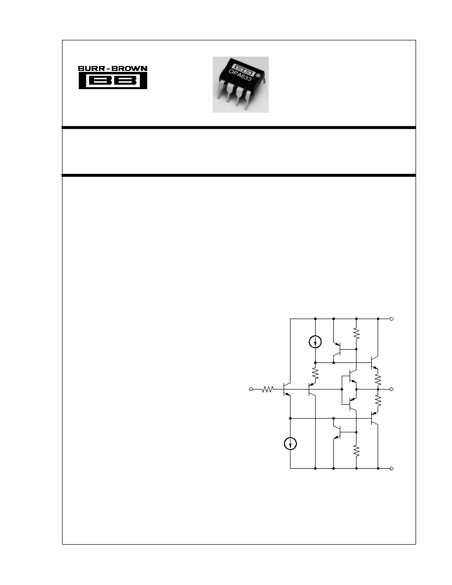
OPA633
High Speed
BUFFER AMPLIFIER
DESCRIPTION
The OPA633 is a monolithic unity-gain buffer ampli-
fier featuring very wide bandwidth and high slew rate.
A dielectric isolation process incorporating both NPN
and PNP high frequency transistors achieves perfor-
mance unattainable with conventional integrated cir-
cuit technology. Laser trimming provides low input
offset voltage.
High output current capability allows the OPA633 to
drive 50
and 75
lines, making it ideal for RF, IF
and video applications. Low phase shift allows the
OPA633 to be used inside amplifier feedback loops.
OPA633 is available in a low cost plastic DIP package
specified for 0
∞
C to +75
∞
C operation.
FEATURES
q
WIDE BANDWIDTH: 260MHz
q
HIGH SLEW RATE: 2500V/
µ
s
q
HIGH OUTPUT CURRENT: 100mA
q
LOW OFFSET VOLTAGE: 1.5mV
q
REPLACES HA-5033
q
IMPROVED PERFORMANCE/PRICE:
LH0033, LTC1010, H0S200
APPLICATIONS
q
OP AMP CURRENT BOOSTER
q
VIDEO BUFFER
q
LINE DRIVER
q
A/D CONVERTER INPUT BUFFER
V
OUT
+V
S
≠V
S
V
IN
4
8
1
5
Æ
©
1987 Burr-Brown Corporation
PDS-699B
Printed in U.S.A. October, 1993
2
Æ
OPA633
SPECIFICATIONS
ELECTRICAL
At +25
∞
C, V
S
=
±
12V, R
S
= 50
, R
L
= 100
, and C
L
= 10pF, unless otherwise specified.
OPA633KP
PARAMETER
CONDITIONS
MIN
TYP
MAX
UNITS
FREQUENCY RESPONSE
Small Signal Bandwidth
260
MHz
Full Power Bandwidth
V
O
= 1Vrms, R
L
= 1k
40
MHz
Slew Rate
V
O
= 10V, V
S
=
±
15V, R
L
= 1k
1000
2500
V/
µ
s
Rise Time, 10% to 90%
V
O
= 500mV
2.5
ns
Propagation Delay
1
ns
Overshoot
10
%
Settling Time, 0.1%
50
ns
Differential Phase Error
(1)
0.1
Degrees
Differential Gain Error
(1)
0.1
%
Total Harmonic Distortion
V
O
= 1Vrms, R
L
= 1k
, f = 100kHz
0.005
%
V
O
= 1Vrms, R
L
= 100
, f = 100kHz
0.02
%
OUTPUT CHARACTERISTICS
Voltage
T
A
= T
MIN
to T
MAX
±
8
±
10
V
R
L
= 1k
, V
S
=
±
15V
±
11
±
13
V
Current
±
80
±
100
mA
Resistance
5
TRANSFER CHARACTERISTICS
Gain
0.93
0.95
V/V
R
L
= 1k
0.99
V/V
T
A
= T
MIN
to T
MAX
0.92
0.95
V/V
INPUT
Offset Voltage
T
A
= +25
∞
C
±
5
±
15
mV
T
A
= T
MIN
to T
MAX
±
6
±
25
mV
vs Temperature
±
33
µ
V/
∞
C
vs Supply
T
A
= T
MIN
to T
MAX
54
72
dB
Bias Current
T
A
= +25
∞
C
±
15
±
35
µ
A
T
A
= T
MIN
to T
MAX
±
20
±
50
µ
A
Noise Voltage
10Hz to 1MHz
20
µ
Vp-p
Resistance
1.5
M
Capacitance
1.6
pF
POWER SUPPLY
Rated Supply Voltage
Specified Performance
±
12
V
Operating Supply Voltage
Derated Performance
±
5
±
16
V
Current, Quiescent
I
O
= 0
21
25
mA
I
O
= 0, T
A
= T
MIN
to T
MAX
21
30
mA
TEMPERATURE RANGE
Specification, Ambient
0
+75
∞
C
Operating, Ambient
≠25
+85
∞
C
Junction, Ambient
90
∞
C/W
NOTE: (1) Differential phase error in video transmission systems is the change in phase of a color subcarrier resulting from a change in picture signal from blanked to
white. Differential gain error is the change in amplitude at the color subcarrier frequency resulting from a change in picture signal from blanked to white.
PIN CONFIGURATION
ABSOLUTE MAXIMUM RATINGS
Power Supply,
±
V
S
............................................................................
±
20V
Input Voltage V
IN
...................................................... +V
S
+ 2V to ≠V
S
≠ 2V
Output Current (peak) ...................................................................
±
200mA
Internal Power Dissipation (25
∞
C) .................................................... 1.95W
Junction Temperature ...................................................................... 200
∞
C
Storage Temperature Range ............................................ ≠40
∞
C to +85
∞
C
Lead Temperature (soldering, 10s) .................................................. 300
∞
C
PACKAGE INFORMATION
(1)
PACKAGE DRAWING
MODEL
PACKAGE
NUMBER
OPA633KP
8-Pin Plastic DIP
006
NOTE: (1) For detailed drawing and dimension table, please see end of data
sheet, or Appendix D of Burr-Brown IC Data Book.
TEMPERATURE
MODEL
PACKAGE
RANGE
OPA633KP
8-Pin Plastic DIP
0
∞
C to +75
∞
C
ORDERING INFORMATION
1
2
3
4
8
7
6
5
+V
S
NC
NC
In
Out
NC
Substrate (ground)
≠V
S
Top View
3
Æ
OPA633
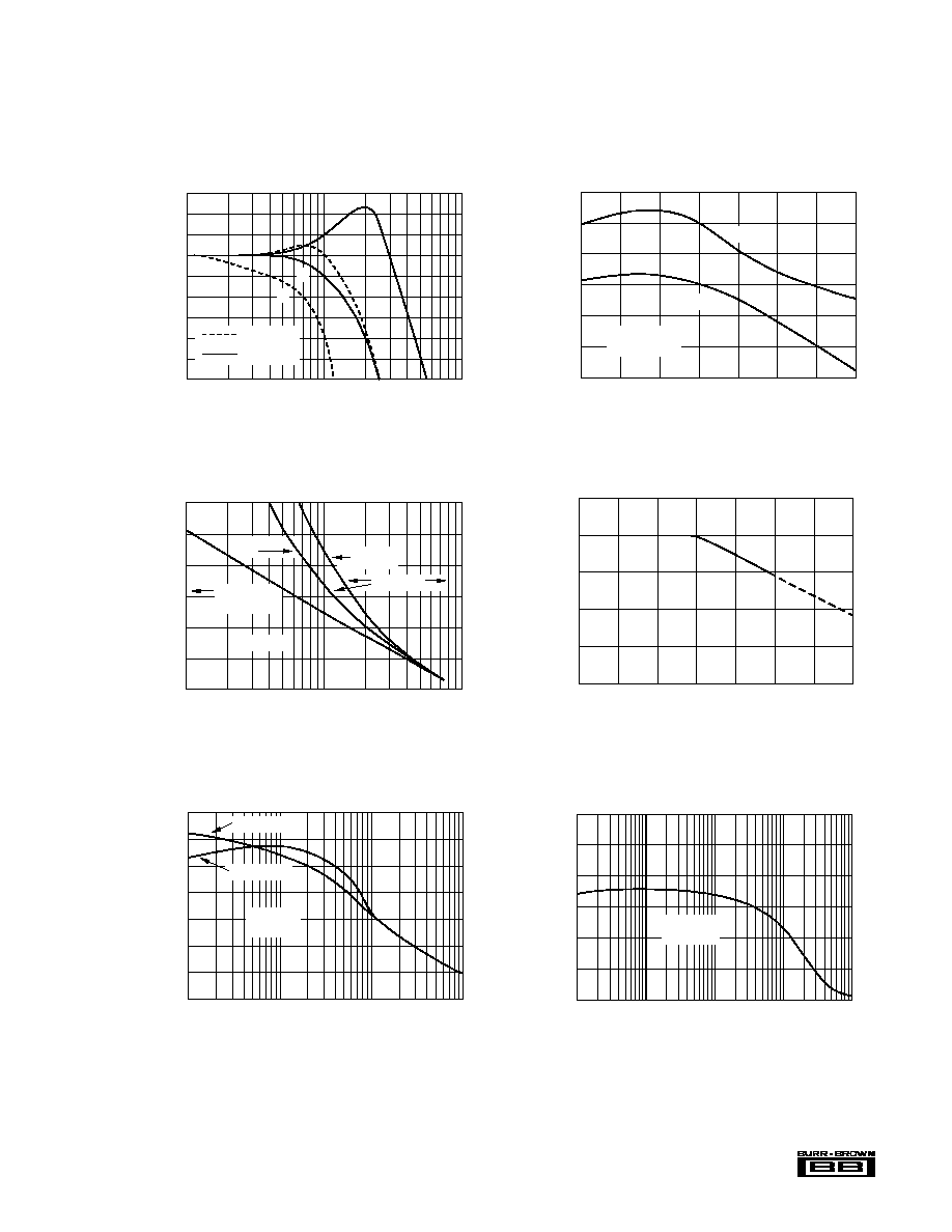
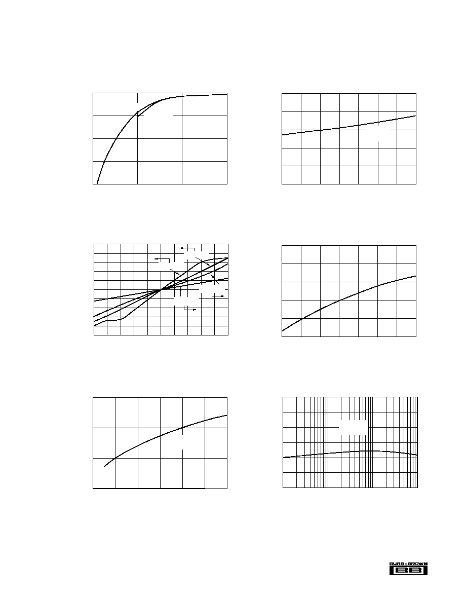
SLEW RATE vs LOAD CAPACITANCE
Load Capacitance (pF)
Slew Rate (V/µs)
3500
3000
2500
2000
1500
1000
500
0
10
1
100
1000
Rising Edge
Falling Edge
V
O
= ±10V
R
L
= 1k
0
Load Capacitance (pF)
SLEW RATE vs LOAD CAPACITANCE
Slew Rate (V/µs)
10,000
10
100
1
1000
3000
2500
2000
1500
1000
500
V
O
= ±10V
R
L
= 100
GAIN/PHASE vs FREQUENCY
Frequency (MHz)
Gain (dB)
6
4
2
0
≠2
≠4
≠6
≠8
≠10
≠12
10
100
1000
R
S
= 300
R
S
= 50
0
≠20
≠40
≠60
≠80
≠100
≠120
Phase (degrees)
SMALL SIGNAL BANDWIDTH vs TEMPERATURE
Temperature (∞C)
Bandwidth (MHz)
300
290
280
270
260
250
240
≠50
50
125
≠25
0
25
75
100
V
S
= ±5V
V
S
= ±15V
V
O
= 0.25Vrms
R
L
= 100
TYPICAL PERFORMANCE CURVES
At +25
∞
C, V
S
=
±
12V, R
S
= 50
, R
L
= 100
, and C
L
= 10pF, unless otherwise specified.
MAXIMUM POWER DISSIPATION
vs AMBIENT TEMPERATURE
Ambient Temperature (∞C)
Power Dissipation (W)
2.5
2.0
1.5
1.0
0.5
0
≠50
50
125
≠25
0
25
75
100
SAFE INPUT VOLTAGE vs FREQUENCY
Frequency (MHz)
Output Voltage (Vp-p)
6
5
4
3
2
1
0
1
10
100
R
L
= 100
R
S
= 1k
Sine Wave
Square Wave
R
L
= 100
(See Text)
6
5
4
3
2
1
0
Output Voltage (Vrms)
4
Æ
OPA633
TYPICAL PERFORMANCE CURVES
(CONT)
At +25
∞
C, V
S
=
±
12V, R
S
= 50
, R
L
= 100
, and C
L
= 10pF, unless otherwise specified.
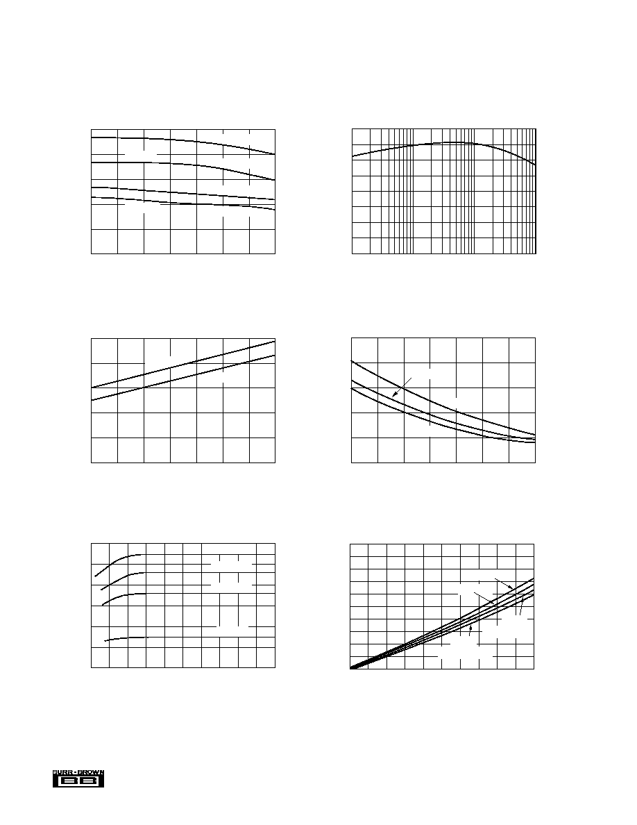
QUIESCENT CURRENT vs TEMPERATURE
Temperature (∞C)
Quiescent Current (mA)
30
25
20
15
10
5
≠50
50
125
≠25
0
25
75
100
V
S
= ±15V
V
S
= ±5V
SLEW RATE vs TEMPERATURE
Temperature (∞C)
Slew Rate (V/µs)
2500
2000
1500
1000
500
0
≠50
50
125
≠25
0
25
75
100
Falling Edge
Rising Edge
Falling Edge
Rising Edge
R
L
= 1k
R
L
= 100
0
Frequency (Hz)
POWER SUPPLY REJECTION vs FREQUENCY
PSRR (dB)
10k
100k
1k
1M
80
70
60
50
40
30
20
10
INPUT BIAS CURRENT vs TEMPERATURE
Temperature (∞C)
I
B
(µA)
25
20
15
10
5
0
≠50
50
125
≠25
0
25
75
100
V
S
= ±15V
V
S
= ±5V
V
S
= ±12V
1.0
0.9
0.8
0.7
0.6
0.5
0.4
0.3
0.2
0.1
0
Output Current (mA)
V
IN
≠ V
OUT
vs OUTPUT CURRENT
V
IN
≠ V
OUT
(V)
20
40
60
80
100
10
30
50
70
90
0
V
O
= ≠10
V
O
= 0
V
O
= +10
V
O
= 0
Current Sourcing
Current Sinking
30
25
20
15
10
5
0
Load Resistance (
)
OUTPUT VOLTAGE SWING vs LOAD RESISTANCE
V
OUT
(Vp-p)
200
400
600
800
1k
100
300
500
700
900
0
V
S
= ±15V
V
S
= ±5V
V
S
= ±10V
V
S
= ±12V
5
Æ
OPA633
TYPICAL PERFORMANCE CURVES
(CONT)
At +25
∞
C, V
S
=
±
12V, R
S
= 50
, R
L
= 100
, and C
L
= 10pF, unless otherwise specified.
OFFSET VOLTAGE vs TEMPERATURE
Temperature (∞C)
V
OS
(mV)
6
4
2
0
≠2
≠4
≠50
50
125
≠25
0
25
75
100
GAIN ERROR vs TEMPERATURE
Temperature (∞C)
V
O
≠ V
IN
(mV)
100
80
60
40
20
0
≠50
50
125
≠25
0
25
75
100
V
O
= ±10V
R
L
= 1k
VOLTAGE GAIN vs LOAD RESISTANCE
Load Resistance (
)
Voltage Gain (V/V)
1.00
0.95
0.90
0.85
0.80
10
10k
100
1k
V
O
= 10Vp-p
f = 1kHz
V
O
= 1Vp-p
1.0
0.8
0.6
0.4
0.2
0
≠0.2
≠0.4
≠0.6
≠0.8
≠1.0
Input Voltage (V)
OUTPUT ERROR vs INPUT VOLTAGE
V
IN
≠ V
OUT
(V)
≠6
≠2
2
6
10
≠8
≠4
0
4
8
≠10
100
80
60
40
20
0
≠20
≠40
≠60
≠80
≠100
V
IN
≠ V
OUT
(mV)
R
L
= 100
R
L
= 1k
R
L
= 50
R
L
= 10k
0.06
0.05
0.04
0.03
0.02
0.01
0
Frequency (Hz)
TOTAL HARMONIC DISTORTION vs FREQUENCY
THD (%)
100k
1k
10k
100
V
O
= 1Vrms
R
L
= 100
TOTAL HARMONIC DISTORTION vs OUTPUT VOLTAGE
Output Voltage (Vrms)
THD (%)
1.0
0.1
0.01
0.001
0
3.0
0.5
2.5
1.0
1.5
2.0
f = 1kHz
R
L
= 100

6
Æ
OPA633
APPLICATIONS INFORMATION
As with any high frequency circuitry, good circuit layout
technique must be used to achieve optimum performance.
Power supply connections must be bypassed with high
frequency capacitors. Many applications benefit from the
use of two capacitors on each power supply--a ceramic
capacitor for good high frequency decoupling and a tanta-
lum type for lower frequencies. They should be located as
close as possible to the buffer's power supply pins. A large
ground plane is used to minimize high frequency ground
drops and stray coupling.
Pin 6 connects to the substrate of the integrated circuit and
should be connected to ground. In principle it could also be
connected to +V
S
or ≠V
S
, but ground is preferable. The
additional lead length and capacitance associated with sock-
ets may cause problems in applications requiring the highest
fidelity of high speed pulses.
Depending on the nature of the input source impedance, a
series input resistor may be required for best stability. This
behavior is influenced somewhat by the load impedance
(including any reactive effects). A value of 50
to 200
is
typical. This resistor should be located close to the OPA633's
input pin to avoid stray capacitance at the input which could
reduce bandwidth (see Gain and Phase versus Frequency
curve).
OVERLOAD CONDITIONS
The input and output circuitry of the OPA633 are not
protected from overload. When the input signal and load
characteristics are within the devices's capabilities, no pro-
tection circuitry is required. Exceeding device limits can
result in permanent damage.
The OPA633's small package and high output current capa-
bility can lead to overheating. The internal junction tempera-
ture should not be allowed to exceed 150
∞
C. Although
failure is unlikely to occur until junction temperature
exceeds 200
∞
C, reliability of the part will be degraded
significantly at such high temperatures. Since significant
heat transfer takes place through the package leads, wide
printed circuit traces to all leads will improve heat sinking.
Sockets reduce heat transfer significantly and are not recom-
mended.
Junction temperature rise is proportional to internal power
dissipation. This can be reduced by using the minimum
supply voltage necessary to produce the required output
voltage swing. For instance, 1V video signals can be easily
handled with
±
5V power supplies thus minimizing the
internal power dissipation.
Output overloads or short circuits can result in permanent
damage by causing excessive output current. The 50
or
75
series output resistor used to match line impedance
will, in most cases, provide adequate protection. When this
resistor is not used, the device can be protected by limiting
the power supply current. See "Protection Circuits."
Excessive input levels at high frequency can cause increased
internal dissipation and permanent damage. See the safe
input voltage versus frequency curves. When used to buffer
an op amp's output, the input to the OPA633 is limited, in
most cases, by the op amp. When high frequency inputs can
exceed safe levels, the device must be protected by limiting
the power supply current.
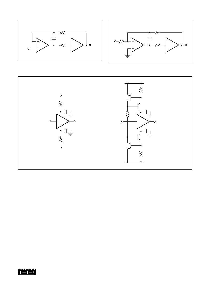
PROTECTION CIRCUITS
The OPA633 can be protected from damage due to exces-
sive currents by the simple addition of resistors in series with
the power supply pins (Figure 5a). While this limits output
current, it also limits voltage swing with low impedance
loads. This reduction in voltage swing is minimal for AC or
high crest factor signals since only the average current from
the power supply causes a voltage drop across the series
resistor. Short duration load-current peaks are
supplied by the bypass capacitors.
The circuit of Figure 5b overcomes the limitations of the
previous circuit with DC loads. It allows nearly full output
voltage swing up to its current limit of approximately 140mA.
Both circuits require good high frequency capacitors (e.g.,
tantalum) to bypass the buffer's power supply connections.
CAPACITIVE LOADS
The OPA633 is designed to safely drive capacitive loads up
to 0.01
µ
F. It must be understood, however, that rapidly
changing voltages demand large output load currents:
I
LOAD
= C
LOAD
Thus, a signal slew rate of 1000V/
µ
s and load capacitance of
0.01
µ
F demands a load current of 10A. Clearly maximum
slew rates cannot be combined with large capacitive loads.
Load current should be kept less than 100mA continuous
(200mA peak) by limiting the rate of change of the input
signal or reducing the load capacitance.
USE INSIDE A FEEDBACK LOOP
The OPA633 may be used inside the feedback path of an op
amp such as the OPA602. Higher output current is achieved
without degradation in accuracy. This approach may actu-
ally improve performance in precision applications by re-
moving load-dependent dissipation from a precision op amp.
All vestiges of load-dependent offset voltage and tempera-
ture drift can be eliminated with this technique. Since the
buffer is placed within the feedback loop of the op amp, its
DC errors will have a negligible effect on overall accuracy.
Any DC errors contributed by the buffer are divided by the
loop gain of the op amp.
The low phase shift of the OPA633 allows its use inside the
feedback loop of a wide variety of op amps. To assure
stability, the buffer must not add significant phase shift to
the loop at the gain crossing frequency of the circuit--the
frequency at which the open loop gain of the op amp is equal
to the closed loop gain of the application. The OPA633 has
a typical phase shift of less than 10
∞
up to 70MHz, thus
making it useful even with wideband op amps.
dV
dt
7
Æ
OPA633
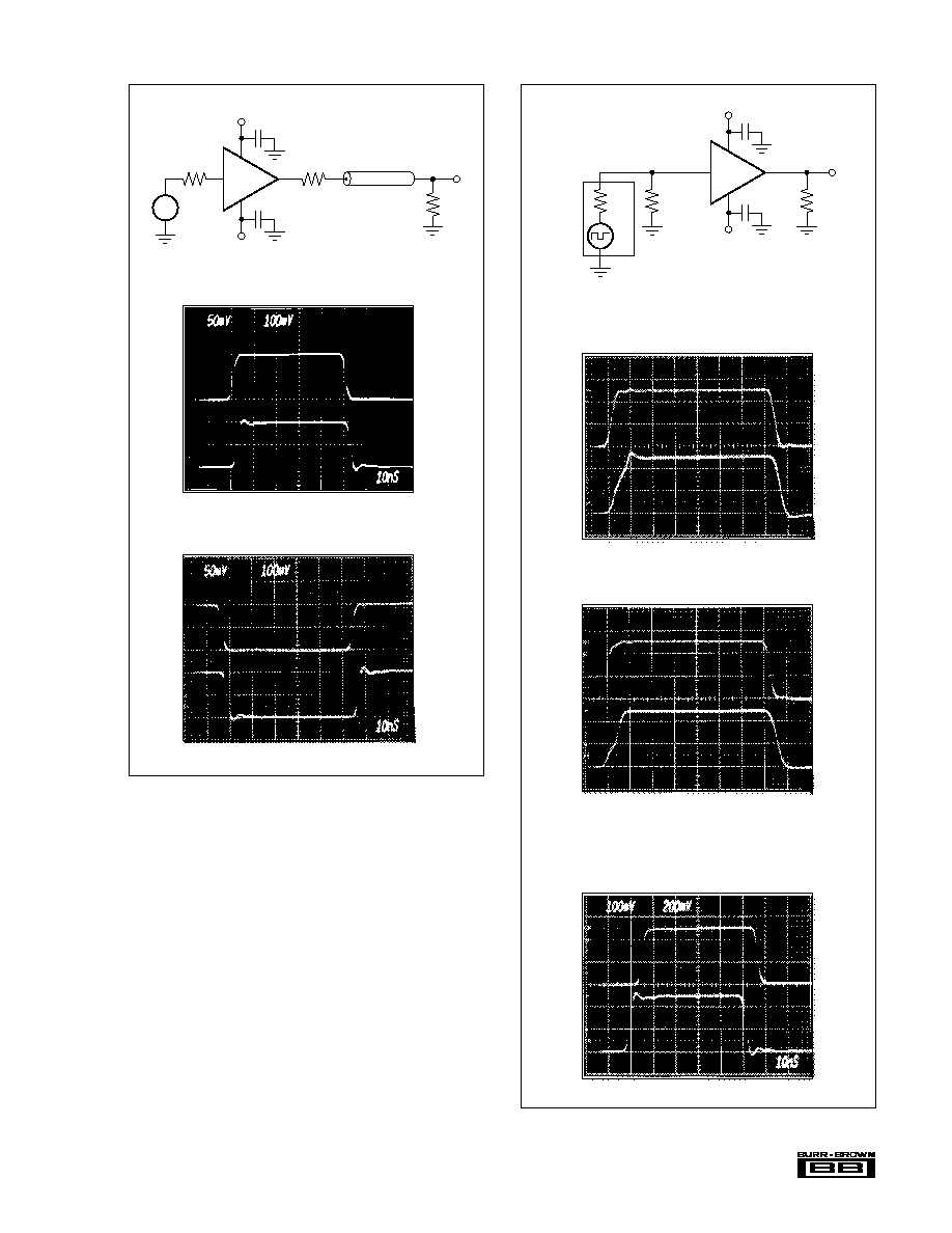
LARGE SIGNAL RESPONSE
10V STEP -- R
L
= 1k
10ns/div
10V STEP -- R
L
= 100k
10ns/div
SMALL SIGNAL RESPONSE
0.5V STEP -- R
L
= 1k
FIGURE 2. Dynamic Response Test Circuit.
OPA633
R
10
R
L
C
1
0.1µF
C
4
0.1µF
+15V
≠15V
V
OUT
R
5
50
50
Pulse
Generator
V
IN
Termination
10V
V
IN
0
10V
V
OUT
0
10V
V
IN
0
10V
V
OUT
0
0.5V
V
IN
0
0.5V
V
OUT
0
FIGURE 1. Coaxial Cable Driver Circuit.
NEGATIVE PULSE RESPONSE
0
V
IN
≠100mV
0
V
OUT
≠50mV
POSITIVE PULSE RESPONSE
100mV
V
IN
0
50mV
V
OUT
0
OPA633
R
10
50
RG-58
Coaxial Cable
R
2
50
C
1
0.1µF
C
4
0.1µF
R
1
180
+12V
≠12V
V
IN
8
Æ
OPA633
The information provided herein is believed to be reliable; however, BURR-BROWN assumes no responsibility for inaccuracies or omissions. BURR-BROWN
assumes no responsibility for the use of this information, and all use of such information shall be entirely at the user's own risk. Prices and specifications are subject
to change without notice. No patent rights or licenses to any of the circuits described herein are implied or granted to any third party. BURR-BROWN does not
authorize or warrant any BURR-BROWN product for use in life support devices and/or systems.
FIGURE 3. Precision High Current Buffer.
FIGURE 4. Buffered Inverting Amplifier.
FIGURE 5. Output Protection Circuits.
OPA633
1µF
1µF
≠V
S
+
+
Tantalum
Tantalum
Output
+V
S
100
100
Input
(a)
OPA633
1µF
1µF
≠V
S
+
+
Tantalum
Tantalum
Output
+V
S
4.7
2.7k
Input
(b)
4.7
OPA633
C
5
500pF
R
8
150
R
9
1k
OPA602
OPA633
C
5
50pF
R
8
150
R
9
10k
OPA602
G = ≠10
R
4
1k