 | –≠–ª–µ–∫—Ç—Ä–æ–Ω–Ω—ã–π –∫–æ–º–ø–æ–Ω–µ–Ω—Ç: PCM1704U | –°–∫–∞—á–∞—Ç—å:  PDF PDF  ZIP ZIP |

24-Bit, 96kHz
BiCMOS Sign-Magnitude
DIGITAL-TO-ANALOG CONVERTER
49%
FPO
International Airport Industrial Park ∑ Mailing Address: PO Box 11400, Tucson, AZ 85734 ∑ Street Address: 6730 S. Tucson Blvd., Tucson, AZ 85706 ∑ Tel: (520) 746-1111 ∑ Twx: 910-952-1111
Internet: http://www.burr-brown.com/ ∑ FAXLine: (800) 548-6133 (US/Canada Only) ∑ Cable: BBRCORP ∑ Telex: 066-6491 ∑ FAX: (520) 889-1510 ∑ Immediate Product Info: (800) 548-6132
PCM1704
Æ
FEATURES
q
SAMPLING FREQUENCY (f
S
): 16kHz to 96kHz
q
8X OVERSAMPLING AT 96kHz
q
INPUT AUDIO DATA WORD: 20-, 24-Bit
q
HIGH PERFORMANCE:
Dynamic Range: K Grade = 112dB typ
SNR: 120dB typ
THD+N: K Grade = 0.0008% typ
q
FAST CURRENT OUTPUT:
±
1.2mA/200ns
q
GLITCH-FREE OUTPUT
q
PIN-PROGRAMMABLE DATA INVERSION
q
POWER SUPPLY:
±
5V
q
SMALL 20-LEAD SO PACKAGE
© 1998 Burr-Brown Corporation
PDS-1454C
Printed in U.S.A. February, 1999
TM
DESCRIPTION
The PCM1704 is a precision, 24-bit digital-to-analog
converter with exceptionally high dynamic perfor-
mance. The ultra-low distortion and excellent low-
level signal performance makes the PCM1704 an ideal
candidate for high-end consumer and professional
audio applications. When used with a digital interpo-
lation filter, the PCM1704 supports 8X oversampling
at 96kHz.
The PCM1704 incorporates a BiCMOS sign-magni-
tude architecture that eliminates glitches and other
nonlinearities around bipolar zero. The PCM1704 is
precision laser-trimmed at the factory to minimize
differential linearity and gain errors.
In addition to high performance audio systems, the
PCM1704 is well-suited to waveform synthesis appli-
cations requiring very low distortion and noise.
Serial Input
and
Control Logic
Reference and Servo
REF DC SERVO DC
DGND +V
DD
≠V
CC
AGND
23-Bit DAC A
23-Bit DAC B
I
OUT
Bipolar Offset
INVERT
20-BIT
WCLK
DATA
BCLK
Power Supply
≠V
DD
+V
CC
BPO DC
PCM1
704
Æ
2
PCM1704
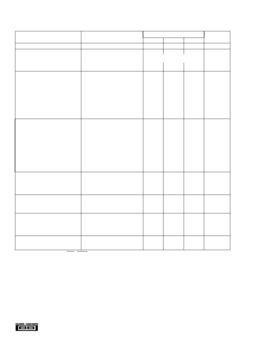
SPECIFICATIONS
All specifications at T
A
= +25
∞
C,
±
V
CC
=
±
V
DD
=
±
5V, f
S
= 768kHz (96kHz ∑ 8), and 24-bit data, unless otherwise noted.
PCM1704U
PARAMETER
CONDITIONS
MIN
TYP
MAX
UNITS
RESOLUTION
24
Bits
DATA FORMAT
Audio Data Interface Format
20-, 24-Bit, MSB-First
Audio Data Code
Binary Two's Complement
Sampling Frequency (f
S
)
16
96
kHz
Input Clock Frequency
25
MHz
DIGITAL INPUT/OUTPUT
Input Logic Level:
V
IH
(1)
+2.0
+5.0
V
V
IL
(1)
0
+0.8
V
V
IH
(2)
≠3.0
0
V
V
IL
(2)
≠5.0
≠4.2
V
Input Logic Current:
I
IH
(1)
V
IH
= +V
DD
±
10
µ
A
I
IL
(1)
V
IL
= 0V
±
10
µ
A
I
IH
(2)
V
IH
= 0V
±
10
µ
A
I
IL
(2)
V
IL
= ≠V
DD
≠100
µ
A
DYNAMIC PERFORMANCE(3)
THD+N
V
O
= 0dB
PCM1704U
0.0025
0.0030
%
PCM1704U-J
0.0015
0.0025
%
PCM1704U-K
0.0008
0.0015
%
V
O
=≠20dB
PCM1704U
0.008
0.020
%
PCM1704U-J
0.007
0.015
%
PCM1704U-K
0.006
0.01
%
Dynamic Range
EIAJ, A-weighted
PCM1704U, U-J
102
110
dB
PCM1704U-K
106
112
dB
Signal-to-Noise Ratio
EIAJ, A-weighted
112
120
dB
Low Level Linearity
f = 1002Hz at ≠90dB
±
0.5
dB
DC ACCURACY
Gain Error
±
1.0
±
3.0
% of FSR
Bipolar Zero Error
±
0.5
±
1.0
% of FSR
Gain Drift
0
∞
C to 70
∞
C
±
25
ppm of FSR/
∞
C
Bipolar Zero Error Drift
0
∞
C to 70
∞
C
±
5
ppm of FSR/
∞
C
ANALOG OUTPUT
Output Range
±
1.2
mA
Output Impedance
1.0
k
Settling Time
±
0.0003% of FSR,
±
1.2mA Step
200
ns
POWER SUPPLY REQUIREMENTS
Voltage Range: +V
CC
= +V
DD
+4.75
+5.0
+5.25
VDC
≠V
CC
= ≠V
DD
≠4.75
≠5.0
≠5.25
VDC
Combined Supply Current:+I
CC
+V
CC
= +V
DD
= +5.0V
5
8
mA
≠I
CC
≠V
CC
= ≠V
DD
= ≠5.0V
30
45
mA
TEMPERATURE RANGE
Operation
≠25
+85
∞
C
Storage
≠55
+125
∞
C
NOTES: (1) BCLK, WCLK, DATA. (2) 20BIT, INVERT. (3) Dynamic performance data is tested with 5534 I/V amp with 7.5k
feedback resistor. THD+N data is
tested by Shibasoku 725C with 30kHz external LPF, 400Hz HPF, average mode. Input signal frequency = 1.1kHz.

Æ
3
PCM1704
PIN ASSIGNMENTS
PIN CONFIGURATION
TOP VIEW
SOIC
PACKAGE INFORMATION
PACKAGE
TEMPERATURE
DRAWING
PRODUCT
PACKAGE
RANGE
NUMBER
(1)
PCM1704U
20-Lead SOIC
≠25
∞
C to +85
∞
C
248
NOTE: (1) For detailed drawing and dimension table, please see end of data
sheet, or Appendix C of Burr-Brown IC Data Book.
ABSOLUTE MAXIMUM RATINGS
Supply Voltage, +V
DD
,+V
CC
............................................................. +6.5V
Supply Voltage Differences ..............................................................
±
0.1V
GND Voltage Differences .................................................................
±
0.1V
Digital Input Voltage
(BCLK, WCLK, DATA) ............................ DGND ≠0.3V to (+V
DD
+ 0.3V)
(20BIT, INVERT) .................................... ≠V
DD
≠ 0.3V to (DGND + 0.3V)
Input Current (any pins except supply pins) ...................................
±
10mA
Power Dissipation .......................................................................... 300mW
Operating Temperature Range ......................................... ≠25
∞
C to +85
∞
C
Storage Temperature ...................................................... ≠55
∞
C to +125
∞
C
Lead Temperature (soldering, 5s) ................................................. +260
∞
C
Package Temperature (reflow, 10s) .............................................. +235
∞
C
PIN
NAME
I/O
FUNCTION
1
DATA
IN
Serial Audio Data Input.
2
BCLK
IN
Bit Clock Input for Serial Audio Data.
3
NC
--
No Connection.
4
≠V
DD
--
Digital Power, ≠5V.
5
DGND
--
Digital Ground.
6
+V
DD
--
Digital Power, +5V.
7
WCLK
IN
Data Latch Enable Input.
8
NC
--
No Connection.
9
20BIT
IN
Input Data Word Selection
(1)
.
10
INVERT
IN
Input Data Polarity Selection
(1)
.
11
+V
CC
--
Analog Power, +5V.
12
BPO DC
--
Bipolar Offset Decoupling Capacitor.
13
NC
--
No Connection.
14
I
OUT
OUT
Current Output for Audio Signal.
15
AGND
--
Analog Ground.
16
AGND
--
Analog Ground.
17
SERVO DC
--
Servo Amplifier Decoupling Capacitor.
18
NC
--
No Connection.
19
REF DC
--
Band Gap Reference Decoupling Capacitor.
20
≠V
CC
--
Analog Power, ≠5V.
NOTE: (1) Internal pull-up resistors. Input level must be a voltage from ≠V
DD
to DGND.
ELECTROSTATIC
DISCHARGE SENSITIVITY
This integrated circuit can be damaged by ESD. Burr-Brown
recommends that all integrated circuits be handled with
appropriate precautions. Failure to observe proper handling
and installation procedures can cause damage.
ESD damage can range from subtle performance degradation
to complete device failure. Precision integrated circuits may
be more susceptible to damage because very small parametric
changes could cause the device not to meet its published
specifications.
1
2
3
4
5
6
7
8
9
10
20
19
18
17
16
15
14
13
12
11
PCM1704U
DATA
BCLK
NC
≠V
DD
DGND
+V
DD
WCLK
NC
20BIT
INVERT
≠V
CC
REF DC
NC
SERVO DC
AGND
AGND
I
OUT
NC
BPO DC
+V
CC
Æ
4
PCM1704
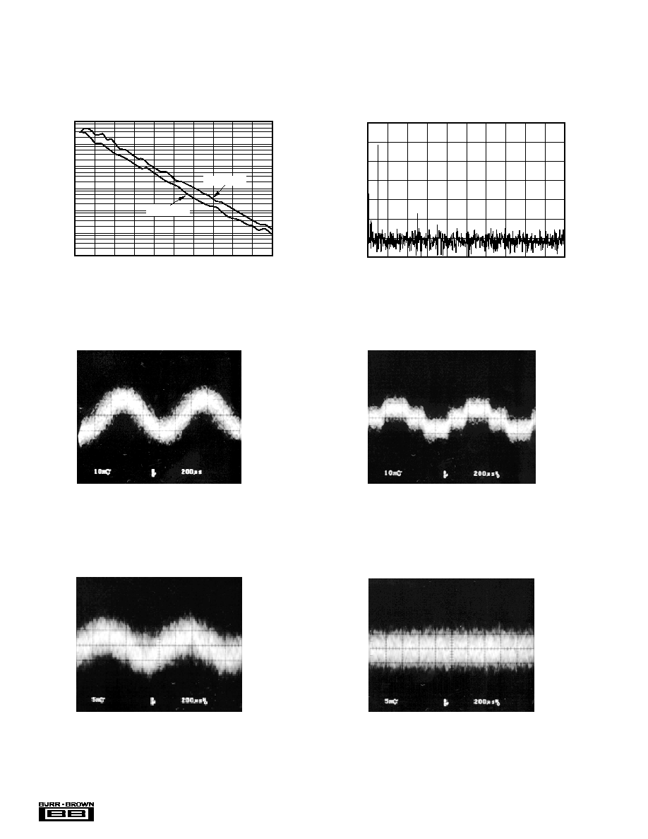
≠90dB SIGNAL SPECTRUM
Output Frequency (Hz)
Amplitude (dB)
≠80
≠90
≠100
≠110
≠120
≠130
≠140
≠150
20.0 2.02k 4.02k 6.01k 8.01k 10.0k 12.0k 14.0k 16.0k 18.0k 20.0k
SPECIFICATIONS
All specifications at +25
∞
C,
±
V
CC
and
±
V
DD
=
±
5.0V, unless otherwise noted.
DAC OUTPUT
≠110dB, 24-Bit, 96kHz
DAC OUTPUT
≠110dB, 20-Bit, 96kHz
DAC OUTPUT
≠120dB, 24-Bit, 96kHz
DAC OUTPUT
≠120dB, 20-Bit, 96kHz
100
10
1
0.1
0.10
0.001
0.0001
0
≠20
≠40
≠60
≠80
≠100
≠120
≠100 ≠90
≠80
≠70
≠60
≠40
≠30
≠10
≠20
≠50
Output Level (dBFS)
THD+N vs LEVEL
THD+N (%)
THD+N (dB)
0
16-Bit Data
24-Bit Data

Æ
5
PCM1704
SPECIFICATIONS (
CONT
)
All specifications at +25
∞
C,
±
V
CC
and
±
V
DD
=
±
5.0V, unless otherwise noted.
≠60
≠70
≠80
≠90
≠100
≠110
≠120
10
20
50
200
500
100
Frequency (Hz)
POWER SUPPLY REJECTION RATIO vs FREQUENCY
Power Supply Rejection Ratio (dB)
1k
≠V
CC
+V
CC

Æ
6
PCM1704
THEORY OF OPERATION
SIGN-MAGNITUDE ARCHITECTURE
Digital audio systems have traditionally used laser-trimmed,
current-source DACs in order to achieve sufficient accuracy.
However, even the best of these suffer from potential low-
level nonlinearity due to errors in the major carry bipolar
zero transition. Current systems have turned to oversampling
data converters, such as the popular delta-sigma architec-
tures, to correct the linearity problems. This is done, how-
ever, at the expense of signal-to-noise performance, and the
noise shaping techniques utilized by these converters creates
a considerable amount of out-of-band noise. If the outputs
are not properly filtered, dynamic performance of the overall
system will be adversely effected.
The PCM1704 employs an innovative architecture which
combines the advantages of traditional DACs (e.g., excellent
full-scale performance, high signal-to-noise ratio, and ease
of use) with superior low-level performance. This architec-
ture is referred to as sign-magnitude. Two DACs are com-
bined in a complementary arrangement to produce an ex-
tremely linear output. The two DACs share a common
reference, and a common R-2R ladder for bit current sources.
The R-2R ladder utilizes dual balanced current segments to
ensure ideal tracking under all conditions. By interleaving
the individual bits of each DAC and employing precision
laser-trimming of resistors, a highly accurate match between
the two DACs is achieved.
The sign-magnitude architecture, which steps away from
zero with small steps in both directions, avoids any glitching
or large linearity errors, and provides an absolute current
output. The low-level performance of the PCM1704 is such
that true 24-bit resolution can be realized around the critical
bipolar zero point.
DISCUSSION OF KEY
SPECIFICATIONS
TOTAL HARMONIC DISTORTION + NOISE (THD+N)
This is the key specification for the PCM1704. Digital data
words are read into the PCM1704 at eight times the standard
DVD audio sampling frequency of 96kHz (e.g., 8 x 96kHz =
768kHz) to create a sinewave output of 1100Hz. The output
of the DAC is then passed through analog signal conditioning
circuitry before being input to a distortion analyzer.
For production testing, the output of the DAC is connected
to a current-to-voltage (I/V) converter. The output of the
I/V converter is then connected to a 40kHz, 3rd-order GIC
low-pass filter. The filter output is then passed on to a
programmable gain amplifier to provide gain for low-level
test signals before being fed into an analog distortion
analyzer (Shiba Soku Model 725 or equivalent).
For the audio bandwidth, the THD+N for the PCM1704 is
essentially flat for all frequencies.
DYNAMIC RANGE
Dynamic range in data converters is specified as the measure
of THD+N at an effective output signal level of ≠60dBFS
(conforms to EIAJ method with A-weighting applied). Reso-
lution is commonly used as a theoretical measure of dy-
namic range, but it does not take into account the effects of
distortion and noise at low signal levels. The sign-magnitude
architecture of the PCM1704, with its ideal performance
around bipolar zero, provides a more usable dynamic range
(even with the strict audio definition) than any other previ-
ously available D/A converter.
IDLE CHANNEL SIGNAL-TO-NOISE RATIO (SNR)
Another important specification for a digital audio converter
is idle channel signal-to-noise ratio (Idle Channel SNR).
This is the ratio of the noise on the DAC output at bipolar
zero compared to the full-scale range of the D/A converter.
To make this measurement, the digital input is continually
fed the code for bipolar zero, while the output of the DAC
is band limited from 20Hz to 20kHz and A-weighting is
applied. The ideal channel SNR for the PCM1704 is typi-
cally greater than 120dB, making it ideal for low noise
applications.
OFFSET GAIN AND TEMPERATURE DRIFT
Although the PCM1704's primary application is in high
performance digital audio systems where dynamic specifica-
tions are most important, specifications are also given for
more traditional DC parameters. These include gain error,
bipolar zero offset, temperature gain and offset drift. These
specifications are important in test and measurement sys-
tems, which is the other main systems application for the
PCM1704.

Æ
7
PCM1704
AUDIO DATA INTERFACE
BASIC OPERATION
The audio interface of the PCM1704 accepts TTL-compat-
ible input levels. The data format at the DATA input of the
PCM1704 is Binary Two's Complement, with the most
significant bit (MSB) being first in the serial input bit steam.
Table I shows the relationship between the audio input data
and DAC output for the PCM1704. Any number of bits can
precede the 24 bits to be loaded since only the last 24 bits
will be transferred to the parallel DAC register after WCLK
(pin 7) has gone LOW (logic 0).
Maximum Bit Clock (BCLK) Rate
The maximum BCLK rate is specified as 25MHz. This is
derived from the 8X oversampling of the PCM1704. Given
a 96kHz sampling rate, an 8X oversampling input and a
32-bit frame length, we get:
96kHz ∑ 8 ∑ 32 = 24.576MHz
"Stopped Clock" Operation
The PCM1704 is normally operated with a continuous
BCLK input. If BCLK is stopped between input data words,
the last 24 bits shifted in are not actually transferred from the
serial register to the parallel DAC register until WCLK goes
LOW. WCLK must remain LOW until after the first BCLK
cycle of the next data word to insure proper DAC operation.
The specified setup and hold times for DATA and WCLK
must be observed.
DATA FORMAT CONTROL
Data format is controlled by two pins on the PCM1704--the
20BIT and INVERT inputs. Their functions are described in
the following paragraphs and tables.
Input Word Length
20BIT (pin 9) is used to select the input data length. Table
II shows the available selections. Pin 9 is internally pulled
up to DGND and therefore, defaults to 24-bit data.
BINARY TWO'S COMPLEMENT
INPUT DATA (Hex)
DAC OUTPUT
7FFFFF
+ Full Scale
000000
Bipolar Zero
FFFFFF
Bipoar Zero ≠ 1 LSB
800000
≠ Full Scale
TABLE I. Digital Input/DAC Output Relationships.
Audio data is supplied to the DATA (pin 1) input. The bit
clock is used to shift data into the PCM1704 and is supplied
to BCLK (pin 2). All DAC serial input data bits are latched
into the serial input register on the rising edge of BCLK. The
serial-to-parallel data transfer to the DAC occurs on the
falling edge of WCLK. The change in the output of the DAC
occurs at the rising edge of the 2nd BCLK after the falling
edge of WCLK. Figure 1 shows the audio data input format.
Figure 2 shows the input timing relationships.
FIGURE 1. Audio Input Data Format.
t
DS
t
BCH
t
BCY
t
DH
t
BCL
t
WCH
t
WCL
t
WH
t
WS
1.4V
1.4V
1.4V
WCLK
BCLK
DATA
FIGURE 2. Audio Input Data Timing.
BCLK Pulse Cycle Time
t
BCY
40ns
(min)
BCLK Pulse Width HIGH
t
BCH
14ns
(min)
BCLK Pulse Width LOW
t
BCL
14ns
(min)
BCLK Rising Edge to WCLK Falling Edge
t
WH
10ns
(min)
WCLK Falling Edge to BCLK Rising Edge
t
WS
10ns
(min)
WCLK Pulse Width HIGH
t
WCH
> t
BCY
WCLK Pulse WIdth LOW
t
WCL
> t
BCY
DATA Set-up Time
t
DS
10ns
(min)
DATA Hold Time
t
DH
10ns
(min)
20BIT (Pin 9)
DATA WORD LENGTH
20BIT = H (DGND)
24-Bit Data Word
20BIT = L (≠V
DD
)
20-Bit Data Word
TABLE II. Input Word Length Selection.
B1 B2 B3
B22 B23
MSB
LSB
B24
WCLK
DATA
DAC Output
BCK
DATA (20-Bit)
DATA (24-Bit)
LSB
B1 B2 B3
B18 B19
MSB
B20
Æ
8
PCM1704
Input Data Inversion
INVERT (pin 10) is used to select the phase of the input data
presented to the DAC. Table III shows the two options. Pin
10 is internally pulled up to DGND, and therefore defaults
to normal, or non-inverting data.
APPLICATIONS INFORMATION
POWER SUPPLIES
For this discussion, please refer to the internal connection
diagram for the PCM1704 in Figure 3. The PCM1704 only
requires a
±
5V supply for operation. Both positive supplies
(+V
DD
and +V
CC
) should be tied together at a single point
and connected to a single +5V analog power supply. Simi-
larly, both negative supplies (≠V
DD
and ≠V
CC
) should be tied
at a single point and connected to a single ≠5V analog power
INVERT (Pin 10)
PHASE
INVERT = H (DGND)
Normal (non-inverted)
INVERT = L (≠V
DD
)
Inverted
TABLE III. Input Data Phase Selection.
supply. No advantage is gained by using separate analog and
digital power supplies. It is more important that the analog
supplies used to drive these pins are as noise and ripple free
as possible to reduce coupling of supply noise to the output.
Power supply decoupling capacitors should be used at each
supply pin to maximize power supply rejection, as shown in
Figure 3. All ground pins (AGND and DGND) should be
connected to an analog ground plane as close to the PCM1704
as possible. The PCM1704 should reside entirely over the
analog ground plane of the printed circuit board.
Bypass and Decoupling Capacitor Requirements
Various-sized decoupling capacitors can be used, with no
special tolerances being required. Figure 5 shows typical
values used by Burr-Brown on our evaluation fixture, which
designers can use as recommended values. All capacitors
should be located as close to the appropriate pins of the
PCM1704 as possible to reduce noise pickup from sur-
rounding circuitry. Aluminum electrolytic capacitors are
recommended for larger values, while metal-film or mono-
lithic ceramic capacitors are used for smaller values.
FIGURE 3. PCM1704 Internal Connection Diagram.
Interface
Logic
and
Logic Bias
23-Bit
Segment
Switches
Reference,
Servo
and
Bipolar
Offset
Analog
Bias
Logic
Bias
23-Bit
Current
Segments
BPO
DGND
≠V
CC
AGND
I
OUT
BCLK
WCLK
DATA
≠V
DD
+V
DD
+V
CC
+5V Supply
BPO DC
SERVO DC
REF DC
+
+
+
+
+
+
+
≠5V Supply
2mA
3mA
20mA
10mA
Æ
9
PCM1704
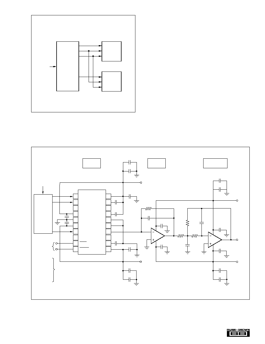
FIGURE 4. Audio Interface Connections for Stereo Audio
Application.
FIGURE 5. Typical Application Circuit (one channel shown).
DOR
WCKO
BCKO
DOL
DATA
WCLK
BCLK
DATA
WCLK
BCLK
DF1704 or Other
Digital Filter
PCM1704
PCM1704
24-Bit
96kHz
Data
TYPICAL APPLICATION
EXAMPLES
The audio interface connections for a stereo audio applica-
tion is shown in Figure 4. The audio data is input to the
digital filter, which then oversampleS the data by a factor of
8. The audio data is then filtered digitally and output to the
PCM1704 DACs.
Figure 5 shows single channel circuit connections for a
typical PCM1704 application. It shows the PCM1704 inter-
face to the digital filter, the I/V converter, and the DAC post
filter. Selection of an appropriate op amp for the I/V con-
verter is critical for obtaining optimum dynamic perfor-
mance from the PCM1704. The OPA627 is recommended
for this application. Op amps with similar characteristics and
faster settling times may also be used.
The suggested DAC post filter is a second-order lowpass
active filter, using the multiple feedback (MFB) circuit
technique. The OPA2134 is an excellent choice for the op
amp in this circuit, since it is designed for high performance
audio applications. The post filter is used to reconstruct and
band limit the DAC output signal.
20
19
18
17
16
15
14
13
12
11
1
2
3
4
5
6
7
8
9
10
C
1
C
2
C
4
C
3
C
5
+
Digital
Controls
Aluminum
Electrolytics
≠5V
100
µ
F
0.1
µ
F
+
C
7
+
+
+
4.7
µ
F
OPA627
1/2
OPA2134
47pF
+
4.7
µ
F
+
C
6
+
+
100
µ
F
0.1
µ
F
+
100
µ
F
0.1
µ
F
+
+5V
≠15V
Audio
Output
+15V
100
µ
F
0.1
µ
F
+
PCM1704U
DATA
BCLK
NC
≠V
DD
DGND
+V
DD
WCLK
NC
20BIT
INVERT
≠V
CC
REF DC
NC
SERVO DC
AGND
AGND
I
OUT
NC
BPO DC
+V
CC
8X
Oversampling
Interpolation
Filter
2.5k
U1
U2
4.7k
4.7k
2k
4.7
µ
F
560pF
2200pF
+
4.7
µ
F
+
DAC
I/V
Post Filter
24-Bit
96kHz Data
C
1
= 4.7
µ
F
C
2
= 4.7
µ
F
C
3
= 4.7
µ
F
C
4
= 47
µ
F
C
5
= 47
µ
F
C
6
= 100
µ
F
C
7
= 4.7