 | –≠–ª–µ–∫—Ç—Ä–æ–Ω–Ω—ã–π –∫–æ–º–ø–æ–Ω–µ–Ω—Ç: PCM1717 | –°–∫–∞—á–∞—Ç—å:  PDF PDF  ZIP ZIP |

Æ
1
PCM1717
49%
FPO
PCM1717
Æ
Stereo Audio
DIGITAL-TO-ANALOG CONVERTER
FEATURES
q
ACCEPTS 16- OR 18-BIT INPUT DATA
q
COMPLETE STEREO DAC:
8X Oversampling Digital Filter
Multi-Level Delta-Sigma DAC
Analog Low Pass Filter
Output Amplifier
q
HIGH PERFORMANCE:
≠90dB THD+N
96dB Dynamic Range
100dB SNR
q
SYSTEM CLOCK: 256fs or 384fs
q
WIDE POWER SUPPLY: +2.7V to +5.5V
q
SELECTABLE FUNCTIONS:
Soft Mute
Digital Attenuation (256 Steps)
Digital De-emphasis
Output Mode: L, R, Mono, Mute
q
SMALL SSOP-20 PACKAGE
DESCRIPTION
The PCM1717 is a complete low cost stereo, audio
digital-to-analog converter, including digital interpo-
lation filter, 3rd-order delta-sigma DAC, and analog
output amplifiers. PCM1717 is fabricated on a highly
advanced 0.6
µ
CMOS process. PCM1717 accepts
16- or 18-bit normal input data format, or 16- or
18-bit I
2
S data format.
The digital filter performs an 8X interpolation func-
tion, as well as special functions such as soft mute,
digital attenuation, and digital de-emphasis. The digi-
tal filter features ≠35dB stop band attenuation and
±
0.17dB ripple in the pass band.
PCM1717 is suitable for a wide variety of cost-sensitive
consumer applications where good performance is re-
quired. Its low cost, small size, and single +5V power
supply make it ideal for automotive CD players, book-
shelf CD players, BS tuners, keyboards, MPEG audio,
MIDI applications, set-top boxes, CD-ROM drives,
CD-Interactive, and CD-Karaoke systems.
Æ
PCM1717
Serial
Input
I/F
Mode
Control
I/F
8X Oversampling
Digital Filter with
Multi Function
Control
Clock/OSC Manager
XTI XTO
CLKO
V
CC
AGND
V
DD
DGND
Multi-level
Delta-Sigma
Modulator
V
OUT
L
D/C_L
Open Drain
DAC
Multi-level
Delta-Sigma
Modulator
Output Amp
and
Low-pass
Filter
Output Amp
and
Low-pass
Filter
BPZ-Cont.
V
OUT
R
D/C_R
ZERO
DAC
MC/DM0
MD/DM1
ML/MUTE
LRCIN
DIN
BCKIN
Reset
MODE
RSTB
Power Supply
© 1995 Burr-Brown Corporation
PDS-1289D
Printed in U.S.A. March, 2000
For most current data sheet and other product
information, visit www.burr-brown.com
International Airport Industrial Park ∑ Mailing Address: PO Box 11400, Tucson, AZ 85734 ∑ Street Address: 6730 S. Tucson Blvd., Tucson, AZ 85706 ∑ Tel: (520) 746-1111
Twx: 910-952-1111 ∑ Internet: http://www.burr-brown.com/ ∑ Cable: BBRCORP ∑ Telex: 066-6491 ∑ FAX: (520) 889-1510 ∑ Immediate Product Info: (800) 548-6132

Æ
2
PCM1717
SPECIFICATIONS
All specifications at +25
∞
C, +V
CC
= +V
DD
= +5V, fs = 44.1kHz, and 16-bit input data, SYSCLK = 384fs, unless otherwise noted. Measurement bandwidth is 20kHz.
PCM1717E
PARAMETER
CONDITIONS
MIN
TYP
MAX
UNITS
RESOLUTION
16
18
Bits
DIGITAL INPUT/OUTPUT
Logic Family
CMOS
Input Logic Level:
V
IH
(2)
70% of V
DD
V
V
IL
(2)
30% of V
DD
V
V
IH
(3)
70% of V
DD
V
V
IL
(3)
30% of V
DD
V
V
IH
(4)
64% of V
DD
V
V
IL
(4)
28% of V
DD
V
Input Logic Current:
I
IH
(5)
≠6.0
µ
A
I
IL
(5)
≠120
µ
A
I
IH
(6)
≠2
µ
A
I
IL
(6)
0.02
µ
A
I
IH
(4)
V
IN
= 3.2V
40
µ
A
I
IL
(4)
V
IN
= 1.4V
≠40
µ
A
Output Logic Level: (+V
DD
= +5V)
V
OH
(7)
I
OH
= ≠5mA
3.8
V
V
OL
(7)
I
OL
= +5mA
1.0
V
V
OL
(8)
I
OL
= +5mA
1.0
V
Interface Format
Selectable Normal, I
2
S
Data Format
16/18 Bits MSB First Binary Two's Complement
Sampling Frequency
32
44.1
48
kHz
System Clock Frequency
256fs/384fs
8.192/12.288
11.2896/16.9344
12.288/18.432
MHz
DC ACCURACY
Gain Error
±
1.0
±
5.0
% of FSR
Gain Mismatch Channel-to-Channel
±
1.0
±
5.0
% of FSR
Bipolar Zero Error
V
O
= 1/2 V
CC
at Bipolar Zero
±
30
mV
DYNAMIC PERFORMANCE
(1)
V
CC
= +5V, f = 991Hz
THD+N at FS (0dB)
≠90
≠80
dB
THD+N at ≠60dB
≠34
dB
Dynamic Range
EIAJ, A-weighted
90
96
dB
Signal-To-Noise Ratio
EIAJ, A-weighted
92
100
dB
Channel Separation
90
97
dB
Level Linearity Error (≠90dB)
±
0.5
dB
DYNAMIC PERFORMANCE
(1)
V
CC
= +3V, f = 991Hz
THD+N at FS (0dB)
≠86
dB
Dynamic Range
EIAJ, A-weighted
91
dB
Signal-To-Noise Ratio
EIAJ, A-weighted
94
dB
DIGITAL FILTER PERFORMANCE
Pass Band Ripple
±
0.17
dB
Stop Band Attenuation
≠35
dB
Pass Band
0.445
fs
Stop Band
0.555
fs
De-emphasis Error
(fs = 32kHz ~ 48kHz)
≠0.2
+0.55
dB
Delay Time (Latency)
11.125/fs
sec
ANALOG OUTPUT
Voltage Range
FS (0dB) OUT
62% of V
CC
Vp-p
Load Impedance
5
k
Center Voltage
50% of V
CC
V
POWER SUPPLY REQUIREMENTS
Voltage Range:
+V
CC
+2.7
+5.5
VDC
+V
DD
+2.7
+5.5
VDC
Supply Current: +I
CC
+I
DD
(9)
+V
CC
= +V
DD
= +5V
18.0
25.0
mA
+V
CC
= +V
DD
= +3V
9.0
15.0
mA
Power Dissipation
+V
CC
= +V
DD
= +5V
90
125
mW
+V
CC
= +V
DD
= +3V
27
45
mW
TEMPERATURE RANGE
Operation
≠25
+85
∞
C
Storage
≠55
+100
∞
C
NOTES: (1) Tested with Shibasoku #725 THD. Meter 400Hz HPF, 30kHz LPF On, Average Mode with 20kHz bandwidth limiting. (2) Pins 4, 5, 6, 14: LRCIN, DIN,
BCKIN, FORMAT. (3) Pins 15, 16, 17, 18: RSTB, DM0, DM1, MUTE (Schmitt trigger input). (4) Pin 1: XTI. (5) Pins 15, 16, 17, 18: RSTB, DM0, DM1, MUTE (if
pull-up resistor is used). (6) Pins 4, 5, 6: LRCIN, DIN, BCKIN (if pull-up resistor is not used). (7) Pin 19: CLKO. (8) Pin 7: ZERO. (9) No load on pins 19 (CLKO)
and 20 (XTO).

Æ
3
PCM1717
PIN ASSIGNMENTS
XTI
DGND
V
DD
LRCIN
DIN
BCKIN
ZERO
D/C_R
V
OUT
R
AGND
XTO
CLKO
ML/MUTE
MC/DM1
MD/DM0
RSTB
MODE
DC_L
V
OUT
L
V
CC
1
2
3
4
5
6
7
8
9
10
20
19
18
17
16
15
14
13
12
11
PIN CONFIGURATION
PIN
NAME
FUNCTION
Data Input Interface Pins
4
LRCIN
Sample Rate Clock Input. Controls the update rate (fs).
5
DIN
Serial Data Input. MSB first, right justified (Sony format)
or I
2
S (Philips). Contains a frame of 16- or 18-bit data.
6
BCKIN
Bit Clock Input. Clocks in the data present on DIN input.
Mode Control and Clock Signals
1
XTI
Oscillator Input (External Clock Input). For an internal
clock, tie XTI to one side of the crystal oscillator. For an
external clock, tie XTI to the output of the chosen
external clock.
14
MODE
Operation Mode Select. For Software Mode, tie Mode
"HIGH". For Hardware Mode, tie Mode "LOW".
16
MD/DM0
Mode Control for Data Input or De-emphasis. When
"HIGH" MD is selected, and a "LOW" selects DM0.
17
MC/DM1
Mode Control for BCKIN or De-emphasis. When "HIGH",
MC is selected, and a "LOW" selects DM1.
18
ML/MUTE
Mode Control for Strobe Clock or Mute. When "HIGH",
ML is selected, and a "LOW" selects mute.
19
CLKO
Buffered Output of Oscillator. Equivalent to XTI.
20
XTO
Oscillator Output. When using the internal clock, tie to
the opposite side (from pin 1) of the crystal oscillator.
When using an external clock, leave XTO open.
Operational Controls and Flags
7
ZERO
Infinite Zero Detection Flag, open drain output. When
the zero detection feature is muting the output, ZERO
is "LOW". When non-zero input data is present, ZERO
is in a high impedance state. When the input data is
continuously zero for 65.536 BCKIN cycles, zero will be
low.
15
RSTB
Resets DAC operation with an active "LOW" pulse.
Analog Output Functions
8
D/C_R
Right Channel Output Amplifier Common. Bypass to
ground with 10
µ
F capacitor.
9
V
OUT
R
Right Channel Analog Output. V
OUT
max = 0.62 x V
CC
.
12
V
OUT
L
Left Channel Analog Output. V
OUT
max = 0.62 x V
CC
.
13
D/C_L
Left Channel Output Amplifier Common. Bypass to
ground with 10
µ
F capacitor.
Power Supply Connections
2
DGND
Digital Ground.
3
V
DD
Digital Power Supply (+5V).
10
AGND
Analog Ground.
11
V
CC
Analog Power Supply (+3V).
The information provided herein is believed to be reliable; however, BURR-BROWN assumes no responsibility for inaccuracies or omissions. BURR-BROWN assumes no
responsibility for the use of this information, and all use of such information shall be entirely at the user's own risk. Prices and specifications are subject to change without notice.
No patent rights or licenses to any of the circuits described herein are implied or granted to any third party. BURR-BROWN does not authorize or warrant any BURR-BROWN
product for use in life support devices and/or systems.
Power Supply Voltage ...................................................................... +6.5V
+V
CC
to +V
DD
Difference ...................................................................
±
0.1V
Input Logic Voltage .................................................. ≠0.3V to (V
DD
+ 0.3V)
Power Dissipation .......................................................................... 200mW
Operating Temperature Range ......................................... ≠25
∞
C to +85
∞
C
Storage Temperature ...................................................... ≠55
∞
C to +125
∞
C
Lead Temperature (soldering, 5s) .................................................. +260
∞
C
Thermal Resistance,
JA .......................................................................................
+70
∞
C/W
ABSOLUTE MAXIMUM RATINGS
ELECTROSTATIC
DISCHARGE SENSITIVITY
This integrated circuit can be damaged by ESD. Burr-Brown
recommends that all integrated circuits be handled with
appropriate precautions. Failure to observe proper handling
and installation procedures can cause damage.
ESD damage can range from subtle performance degradation
to complete device failure. Precision integrated circuits may
be more susceptible to damage because very small parametric
changes could cause the device not to meet its published
specifications.
PACKAGE
SPECIFIED
DRAWING
TEMPERATURE
PACKAGE
ORDERING
TRANSPORT
PRODUCT
PACKAGE
NUMBER
RANGE
MARKING
NUMBER
(1)
MEDIA
PCM1717E
SSOP-20
334-1
≠25
∞
C to +85
∞
C
PCM1717E
PCM1717E
Rails
"
"
"
"
"
PCM1717E/2K
Tape and Reel
NOTE: (1) Models with a slash (/) are available only in Tape and Reel in the quantities indicated (e.g., /2K indicates 2000 devices per reel). Ordering 2000 pieces
of "PCM1717E/2K" will get a single 2000-piece Tape and Reel.
PACKAGE/ORDERING INFORMATION
Æ
4
PCM1717
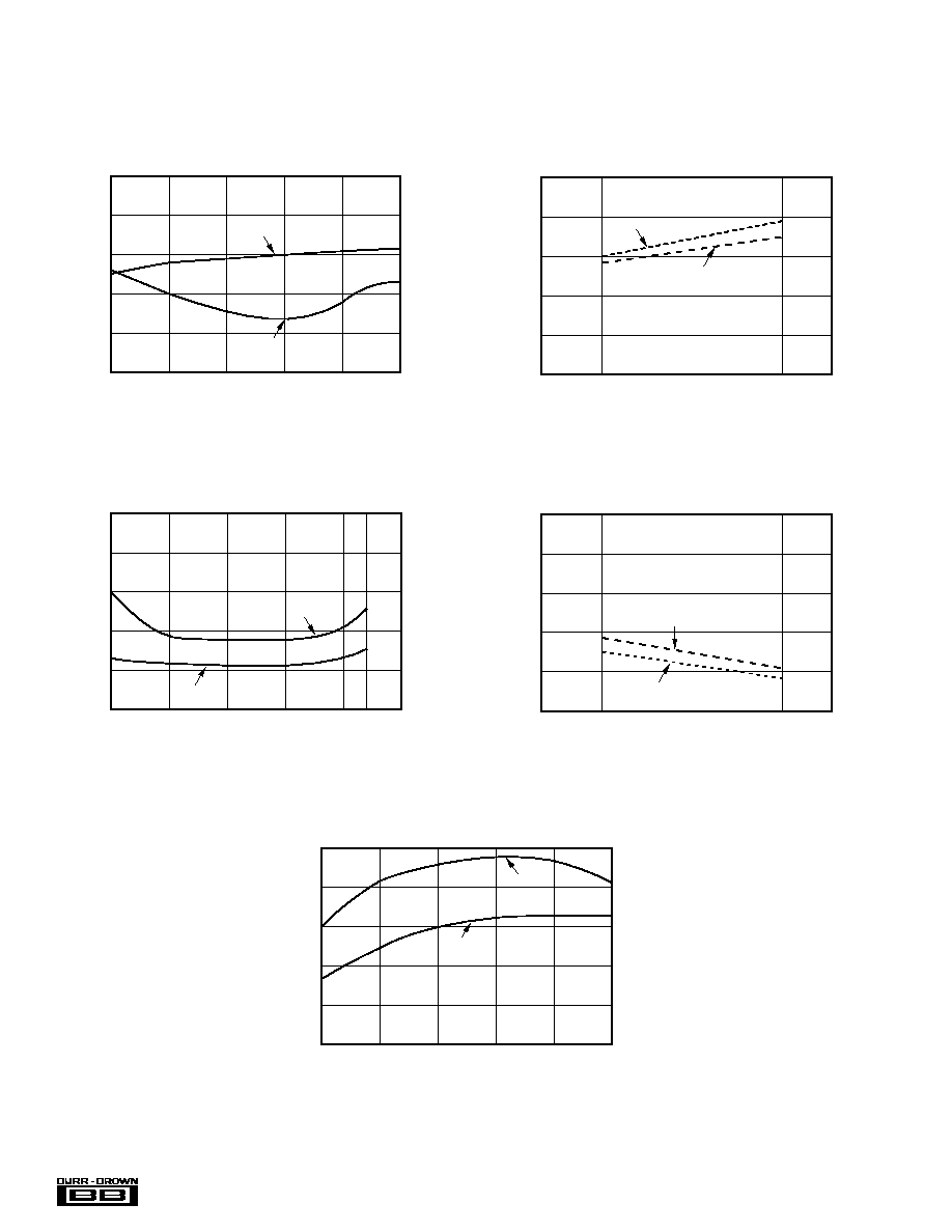
TYPICAL PERFORMANCE CURVES
At T
A
= +25
∞
C, +V
CC
= +V
DD
= +5V, fs = 44.1kHz, and 16-bit input data, SYSCLK = 384fs, unless otherwise noted.
DYNAMIC PERFORMANCE
THD+N vs TEMPERATURE
f
IN
= 1kHz, 384f
S
Temperature (∞C)
THD+N at FS (dB)
THD+N at ≠60dB (dB)
≠84
≠86
≠88
≠90
≠92
≠90
≠30
≠34
≠38
≠25
0
25
50
75
85
100
≠60dB
0dB
DYNAMIC RANGE vs INPUT DATA
f
IN
= 1kHz
Input Data
Dynamic Range (dB)
100
98
96
94
92
90
16-Bit
18-Bit
256f
S
384f
S
THD+N vs INPUT DATA
f
IN
= 1kHz, FS (0dB)
Input Data
THD+N (dB)
≠84
≠86
≠88
≠90
≠92
≠94
16-Bit
18-Bit
256f
S
384f
S
THD+N vs V
CC
, V
DD
f
IN
= 1kHz, 384f
S
V
CC
, V
DD
(V)
THD+N at FS (dB)
THD+N at ≠60dB (dB)
≠84
≠86
≠88
≠90
≠92
≠94
≠30
≠34
≠38
3.0
3.5
4.0
4.5
5.0
5.5
≠60dB
0dB
DYNAMIC RANGE AND SNR vs V
CC
, V
DD
f
IN
= 1kHz, 384f
S
V
CC
, V
DD
(dB)
100
98
96
94
92
90
3.0
3.5
4.0
4.5
5.0
5.5
SNR
Dynamic
Range

Æ
5
PCM1717
TYPICAL PERFORMANCE CURVES
At T
A
= +25
∞
C, +V
CC
= +V
DD
= +5V, fs = 44.1kHz, and 16-bit input data, SYSCLK = 384fs, unless otherwise noted.
DIGITAL FILTER
0 0.4536f
S
1.3605f
S
2.2675f
S
3.1745f
S
4.0815f
S
0
≠20
≠40
≠60
≠80
≠100
dB
OVERALL FREQUENCY CHARACTERISTIC
Frequency (Hz)
0
5k
10k
15k
20k
25k
0
≠2
≠4
≠6
≠8
≠10
≠12
Level (dB)
Frequency (Hz)
DE-EMPHASIS FREQUENCY RESPONSE (32kHz)
DE-EMPHASIS FREQUENCY RESPONSE (44.1kHz)
0
≠2
≠4
≠6
≠8
≠10
≠12
Level (dB)
0
5k
10k
15k
20k
25k
Frequency (Hz)
DE-EMPHASIS FREQUENCY RESPONSE (48kHz)
0
≠2
≠4
≠6
≠8
≠10
≠12
Level (dB)
Frequency (Hz)
0
5k
10k
15k
20k
25k
PASSBAND RIPPLE CHARACTERISTIC
0
≠0.2
≠0.4
≠0.6
≠0.8
≠1
0
0.1134f
S
0.2268f
S
0.3402f
S
0.4535f
S
dB
Frequency (Hz)
0
3628
7256
10884
14512
0.6
0.4
0.2
0
≠0.2
≠0.4
≠0.6
Frequency (Hz)
DE-EMPHASIS ERROR (32kHz)
Error (dB)
0
4999.8375
9999.675
14999.5125
19999.35
0.6
0.4
0.2
0
≠0.2
≠0.4
≠0.6
Frequency (Hz)
DE-EMPHASIS ERROR (44.1kHz)
Error (dB)
0
5442
10884
16326
21768
0.6
0.4
0.2
0
≠0.2
≠0.4
≠0.6
Frequency (Hz)
DE-EMPHASIS ERROR (48kHz)
Error (dB)

Æ
6
PCM1717
SYSTEM CLOCK
The system clock for PCM1717 must be either 256f
S
or
384f
S
, where f
S
is the audio sampling frequency (typically
32kHz, 44.1kHz, or 48kHz). The system clock is used to
operate the digital filter and the modulator.
The system clock can be either a crystal oscillator placed
between XTI (pin 1) and XTO (pin 20), or an external clock
input to XTI. If an external system clock is used, XTO is
open (floating). Figure 1 illustrates the typical system clock
connections.
PCM1717 has a system clock detection circuit which auto-
matically senses if the system clock is operating at 256f
S
or
384f
S
. The system clock should be synchronized with LRCIN
(pin 4) clock. LRCIN (left-right clock) operates at the
sampling frequency fs. In the event these clocks are not
synchronized, PCM1717 can compensate for the phase dif-
ference internally. If the phase difference between left-right
and system clocks is greater than 6 bit clocks (BCKIN), the
synchronization is performed internally. While the synchro-
nization is processing, the analog output is forced to a DC
level at bipolar zero. The synchronization typically occurs in
less than 1 cycle of LRCIN.
DATA INTERFACE FORMATS
Digital audio data is interfaced to PCM1717 on pins 4, 5,
and 6--LRCIN (left-right clock), DIN (data input) and
BCKIN (bit clock). PCM1717 can accept both normal and
I
2
S data formats. Normal data format is MSB first, two's
complement, right-justified. I
2
S data is compatible with
Philips serial data protocol. In the I
2
S format, the data is 16-
or 18-bit, selectable by bit 0 on Register 3 (Software Control
Mode). In the Hardware Mode, PCM1717 can only function
with 16-bit normal data. Figures 5 through 9 illustrate timing
and input formats.
t
XTIH
t
XTIL
1/256f
S
or 1/384f
S
64% OF V
DD
28% OF V
DD
External System Clock High
t
XTIH
10ns (min)
External System Clock Low
t
XTIL
10ns (min)
FIGURE 2. External Clock Timing Requirements.
FIGURE 1. Internal Clock Circuit Diagram and Oscillator Connection.
C
1
C
2
C
1
, C
2
= 10 to 20pF
Internal System Clock
XTI
X'tal
XTO
PCM1717E
CLKO
External Clock
Internal System Clock
XTI
XTO
PCM1717E
EXTERNAL CLOCK INPUT
XTO pin = No Connection
CRYSTAL RESONATOR CONNECTION
CLKO

Æ
7
PCM1717
Reset
PCM1717 has both internal power on reset circuit and the
RSTB-pin (pin 15) which accepts external forced reset by
RSTB = LOW. For internal power on reset, initialize (reset)
is done automatically at power on V
DD
>2.2V (typ). During
internal reset = LOW, the output of the DAC is invalid and
the analog outputs are forced to V
CC
/2. Figure 3 illustrates
the timing of internal power on reset.
For the RSTB-pin, PSTB-pin accepts external forced reset by
RSTB = L. During RSTB = L, the output of the DAC is
invalid and the analog outputs are forced to V
CC
/2 after
internal initialize (1024 system clocks count after RSTB = H.)
Figure 4 illustrates the timing of RSTB-pin reset.
1024 system (= XTI) clocks
Reset
Reset Removal
2.6V
2.2V
1.8V
V
CC
/V
DD
Internal Reset
XTI Clock
FIGURE 3. Internal Power-On Reset Timing.
1024 system (XTI) clocks
Reset
Reset Removal
XTI Clock
Internal Reset
RSTB-pin
50% of V
DD
t
RST
(1)
NOTE: (1) t
RST
= 20ns min
FIGURE 4. RSTB-Pin Reset Timing.

Æ
8
PCM1717
OPERATIONAL CONTROL
PCM1717 can be controlled in two modes. Software Mode
allows the user to control operation with a 16-bit serial
register. Hardware Mode allows the user to hard-wire opera-
tion of PCM1717 using four parallel wires. The MODE pin
determines which mode PCM1717 is in; a LOW level on pin
14 places PCM1717 in Hardware Mode, and a HIGH on pin
14 places PCM1717 in Software Mode.
MODE (Pin 14)
Selected Mode
Pin 16
Pin 17
Pin 18
"HIGH"
Software Mode
MD
MC
ML
"LOW"
Hardware Mode
DM0
DM1
MUTE
Table I indicates which functions are selectable within the
user's chosen mode. All of the functions shown are select-
able in the Software Mode, but only soft mute and de-
emphasis control may be selected in the Hardware Mode.
DIGITAL DE-EMPHASIS (Pins 16 and 17)
Pins 16 and 17 are used as a two-bit parallel register to
control de-emphasis modes:
PIN 16
PIN 17
MODE
0
0
De-emphasis disabled
1
0
De-emphasis enabled at 48kHz
0
1
De-emphasis enabled at 44.1kHz
1
1
De-emphasis enabled at 32kHz
RESET MODE (Pin 15)
A LOW level on pin 15 will force the digital filters, modu-
lators and mode controls into a reset (disable) mode. While
this pin is held low, the output of PCM1717 will be forced
to V
CC
/2 (Bipolar Zero). Bringing pin 15 HIGH will initial-
ize all DAC functions, and allow for normal operation.
SOFTWARE MODE
(Pin 14 = "1")
The Software Mode uses a three-wire interface on pins 16,
17 and 18. Pin 17 (MC) is used to clock in the serial control
data, pin 18 (ML) is used to synchronize the serial control
data, and pin 16 (MD) is used to latch in the serial control
register. There are four distinct registers, with bits 9 and 10
(of 16) determining which register is in use.
REGISTER CONTROL (Bits 9, 10)
REGISTER
B9 (A0)
B10 (A1)
0
0
0
1
1
0
2
0
1
3
1
1
Control data timing is shown in Figure 6. ML is used to latch
the data from the control registers. After each register's
contents are checked in, ML should be taken low to latch in
the data. A "res" in the register indicates that location is
reserved for factory use. When loading the registers, the
"res" bits should be set LOW.
REGISTER 0
Register 0 is used to control left channel attenuation. Bits
0-7 (AL0-AL7) are used to determine the attenuation level.
The level of attenuation is given by:
ATT = [20log
10
(ATT_DATA/255)] dB
B15 B14 B13 B12 B11 B10 B9 B8
B7 B6
B5 B4 B3
B2 B1 B0
res res res res res A1 A0 LDL AL7 AL6 AL5 AL4 AL3 AL2 AL1 AL0
TABLE I. Feature Selections by Mode.
SOFTWARE
HARDWARE
MODE
DEFAULT
MODE
DEFAULT
FUNCTION
SELECTABLE
SELECTABLE
Input Data Format
Yes
No
Normal Format
Normal
Normal Only
Normal
I
2
S Format
Input Resolution
Yes
No
16 Bits
16 Bits
16 Bits Only
16 Bits
18 Bits
LRCIN Polarity
Yes
No
L/R = High/Low
L/R = H/L
L/R = H/L
L/R = H/L
L/R = Low/High
Only
De-emphasis Control
Yes
Yes
32kHz
44.1kHz
OFF
OFF
48kHz
OFF
Soft Mute
Yes
OFF
Yes
OFF
Digital Attenuation
Yes
0dB
No
0dB
Analog Output Mode
Yes
Stereo
No
Stereo
Infinite Zero Detection
Yes
Disabled
No
Disabled
DAC Operation Control
Yes
ON
No
ON
HARDWARE MODE
(Pin 14 = "0")
This mode is controlled by logic levels present on pins 15,
16, 17 and 18. Hardware Mode allows for control of soft
mute, digital de-emphasis and disable ONLY. Other func-
tions such as attenuation, I/O format and infinite zero detect
can only be controlled in the Software Mode.
SOFT MUTE (Pin 18)
A LOW level on pin 18 will force both channels to be muted;
a HIGH level on pin 18 will allow for normal operation.

Æ
9
PCM1717
IZD = 1
IZD = 0
RSTB = "HIGH"
RSTB = "LOW"
SOFTWARE MODE
DATA INPUT
DAC OUTPUT
INPUT
Zero
Forced to BPZ
(1)
Enabled
Other
Forced to BPZ
(1)
Enabled
Zero
Controlled by IZD
Enabled
Other
Normal
Enabled
DATA INPUT
DAC OUTPUT
Zero
Forced to BPZ
(1)
Other
Normal
Zero
Zero
(2)
Other
Normal
Bits 3 (OPE) and 4 (IZD) are used to control the infinite zero
detection features. Tables II through IV illustrate the rela-
tionship between IZD, OPE, and RSTB (reset control):
ATTENUATION DATA LOAD CONTROL
Bit 8 (LDL) is used to control the loading of attenuation data
in B0:B7. When LDL is set to 0, attenuation data will be
loaded into AL0:AL7, but it will not affect the attenuation
level until LDL is set to 1. LDR in Register 1 has the same
function for right channel attenuation. The attenuation level
is given by:
ATT = 20log (y/256) (dB), where y = x, when
0
x
254
y = x + 1, when x = 255
X is the user-determined step number, an integer value
between 0 and 255.
Example:
let x = 255
let x = 254
let x = 1
let x = 0
REGISTER 1
TABLE II. Infinite Zero Detection (IZD) Function.
OPE = 1
OPE = 0
TABLE III. Output Enable (OPE) Function.
SOFTWARE
MODE
DATA INPUT
DAC OUTPUT
INPUT
Zero
Controlled by OPE and IZD
Enabled
Other
Controlled by OPE and IZD
Enabled
Zero
Forced to BPZ
(1)
Disabled
Other
Forced to BPZ
(1)
Disabled
TABLE IV. Reset (RSTB) Function.
NOTE: (1)
is disconnected from output amplifier. (2)
is connected to
output amplifier.
OPE controls the operation of the DAC: when OPE is
"LOW", the DAC will convert all non-zero input data. If the
input data is continuously zero for 65,536 cycles of BCKIN,
the output will only be forced to zero only if IZD is "HIGH".
When OPE is "HIGH", the output of the DAC will be forced
to bipolar zero, irrespective of any input data.
IZD controls the operation of the zero detect feature: when
IZD is "LOW", the zero detect circuit is off. Under this
condition, no automatic muting will occur if the input is
continuously zero. When IZD is "HIGH", the zero detect
feature is enabled. If the input data is continuously zero for
65,536 cycle of BCKIN, the output will be immediately
forced to a bipolar zero state (V
CC
/2). The zero detection
feature is used to avoid noise which may occur when the
input is DC. When the output is forced to bipolar zero, there
may be an audible click. PCM1717 allows the zero detect
feature to be disabled so the user can implement an external
muting circuit.
REGISTER 3
B15 B14 B13 B12 B11 B10 B9 B8
B7
B6 B5
B4
B3
B2
B1
B0
res
res res res
res A1
A0 res PL3 PL2 PL1 PL0 ATC
IW LRP
IIS
Register 3 is used to select the I/O data formats. Bit 0 (IIS)
is used to control the input data format. If the input data
source is normal (16- or 18-bit, MSB first, right-justified),
set bit 0 "LOW". If the input format is IIS, set bit 0 "HIGH".
ATT
=
20 log
0
256
=
≠
ATT
=
20 log
1
256
=
≠ 48.16dB
ATT
=
20 log
254
256
=
≠0. 068dB
ATT
=
20 log
255
+
1
256
=
0dB
B15 B14 B13 B12 B11 B10 B9 B8
B7 B6 B5
B4 B3 B2
B1 B0
res res res res res
A1 A0 LDR AR7 AR6 AR5 AR4 AR3 AR2 AR1 AR0
Register 1 is used to control right channel attenuation. As
in Register 1, bits 0-7 (AR0-AR7) control the level of
attenuation.
REGISTER 2
B15 B14 B13 B12 B11 B10 B9 B8
B7
B6 B5
B4
B3
B2
B1
B0
res res res res
res A1
A0 res
res res res IZD OPE DM1 DM0 MUTE
Register 2 is used to control soft mute, digital de-emphasis,
disable, and infinite zero detect. Bit 0 is used for soft mute;
a HIGH level on bit 0 will cause the output to be muted.
Bits 1 and 2 are used to control digital de-emphasis as
shown below:
BIT 1 (DM0)
BIT 2 (DM1)
DE-EMPHASIS
0
0
De-emphasis disabled
1
0
De-emphasis enabled at 48kHz
0
1
De-emphasis enabled at 44.1kHz
1
1
De-emphasis enabled at 32kHz

Æ
10
PCM1717
DIN (pin 5)
DIN (pin 5)
Audio Data Word = 16-Bit
LRCIN (pin 4)
BCKIN (pin 6)
16
14
MSB
LSB
MSB
LSB
Left-channel Data
Right-channel Data
1 f/s
15
16
1
2
3
16
14
15
1
2
3
14
15
Audio Data Word = 18-Bit
18
16
MSB
LSB
MSB
LSB
17
18
1
2
3
18
16
17
1
2
3
16
17
FIGURE 5. "Normal" Data Input Timing.
FIGURE 6. "I
2
S" Data Input Timing.
DIN (pin 5)
DIN (pin 5)
Audio Data Word = 16-Bit
LRCIN (pin 4)
BCKIN (pin 6)
16
14
MSB
LSB
MSB
LSB
Left-channel Data
Right-channel Data
1 f/s
15
1
2
3
16
14
15
1
2
3
Audio Data Word = 18-Bit
18
16
MSB
LSB
MSB
LSB
17
1
2
3
18
16
17
1
2
3
1
2
1
2
t
BCH
t
BCL
t
LB
t
BCY
t
BL
t
DH
t
DS
50% of V
DD
50% of V
DD
50% of V
DD
LRCIN
BCKIN
DIN
BCKIN Pulsewidth (High Level)
t
BCH
50ns (min)
BCKIN Pulsewidth (Low Level)
t
BCL
50ns (min)
BCKIN Pulse Cycle Time
t
BCY
100ns (min)
BCKIN Rising Edge
®
LRCIN Edge
t
BL
30ns (min)
LRCIN Edge
®
BCKIN Rising Edge
t
LB
30ns (min)
DIN Setup Time
t
DS
30ns (min)
DIN Hold Time
t
DH
30ns (min)
FIGURE 7. Data Input Timing.
Bit 1 is used to select the polarity of LRCIN (sample rate
clock). When bit 1 is LOW, a HIGH state on LRCIN is used
for the left channel, and a LOW state on LRCIN is used for
the right channel. When bit 1 is HIGH the polarity of LRCIN
is reversed.
Bit 2 is used to select the input word length. When bit 2 is
LOW, the input word length is set for 16 bits; when bit 2 is
HIGH, the input word length is set for 18 bits.
Bit 3 is used as an attenuation control. When bit 3 is set
HIGH, the attenuation data on Register 0 is used for both
channels, and the data in Register 1 is ignored. When bit 3
is LOW, each channel has separate attenuation data.
Bits 4 through 7 are used to determine the output format, as
shown in Table V:
PL0
PL1
PL2
PL3
Lch OUTPUT
Rch OUTPUT
NOTE
0
0
0
0
MUTE
MUTE
MUTE
0
0
0
1
MUTE
R
0
0
1
0
MUTE
L
0
0
1
1
MUTE
(L + R)/2
0
1
0
0
R
MUTE
0
1
0
1
R
R
0
1
1
0
R
L
REVERSE
0
1
1
1
R
(L + R)/2
1
0
0
0
L
MUTE
1
0
0
1
L
R
STEREO
1
0
1
0
L
L
1
0
1
1
L
(L + R)/2
1
1
0
0
(L + R)/2
MUTE
1
1
0
1
(L + R)/2
R
1
1
1
0
(L + R)/2
L
1
1
1
1
(L + R)/2
(L + R)/2
MONO
TABLE V. PCM1717 Output Mode Control.
REGISTER RESET STATES
After reset, each register is set to a predetermined state:
Register 0
0000 0000 1111 1111
Register 1
0000 0010 1111 1111
Register 2
0000 0100 0000 0000
Register 3
0000 0110 1001 0000

Æ
11
PCM1717
t
RST
RSTB
RSTB Pulsewidth
20ns (min)
50% of V
DD
FIGURE 10. Typical Connection Diagram of PCM1717.
1
20
4
5
6
14
18
17
16
15
XTI
XTO
LRCIN
DIN
BCKIN
MODE
ML/MUTE
MC/DM1
MD/DM0
RSTB
CLKO
V
OUT
R
D/C_R
D/C_L
V
OUT
L
ZERO
19
9
8
13
12
7
Control
Processor
Mode Control
Reset
PCM
Audio Data
Processor
To External Mute Circuit
10µF
V
DD
4.7k
+
FOUT = Inverted XTI (1 pin)
to Other System
+5V Analog Power Supply
Post
Low Pass
Filter
Post
Low Pass
Filter
10µF
+
0.1µF ~ 10µF
Bypass Capacitor
2
3
DGND
V
DD
10
11
AGND
V
CC
0.1µF ~ 10µF
Bypass Capacitor
10pF ~ 22pF
10pF ~ 22pF
(optional)
(optional)
FIGURE 9. External Reset Timing.
FIGURE 8. Control Data Timing in Software Mode Control.
MC Pulse Cycle
t
MCY
100ns (min)
MC Pulsewidth "L"
t
MCL
50ns (min)
MC Pulse Cycle "H"
t
MCH
50ns (min)
MD Setup Time
t
MDS
30ns (min)
MD Hold Time
t
MDH
30ns (min)
ML Setup Time
t
MLS
30ns (min)
ML Hold Time
t
MLH
30ns (min)
ML Pulsewidth "L"
t
MLL
30ns + 1SYSCLK (min)
ML High Level Time
t
MHH
30ns + 1SYSCLK (min)
t
MCH
t
MCL
t
MCY
t
MLS
t
MLH
t
MDH
t
MDS
t
MLL
t
MHH
50% of V
DD
50% of V
DD
50% of V
DD
B15 B14 B13 B12 B11 B10 B9 B8 B7 B6 B5 B4 B3 B2 B1 B0
ML (pin 18)
MC (pin 17)
MD (pin 16)
ML
MC
MD

Æ
12
PCM1717
Out
48f
S
(384f
S
)
64f
S
(256f
S
)
In
8f
S
18-Bit
+
+
+
4
3
2
1
0
5-level Quantizer
+
≠
+
Z
≠1
+
≠
+
Z
≠1
+
+
Z
≠1
POWER SUPPLY
CONNECTIONS
PCM1717 has two power supply connections: digital (V
DD
)
and analog (V
CC
). Each connection also has a separate
ground. If the power supplies turn on at different times, there
is a possibility of a latch-up condition. To avoid this condi-
tion, it is recommended to have a common connection
between the digital and analog power supplies. If separate
supplies are used without a common connection, the delta
between the two supplies during ramp-up time must be less
than 0.6V.
An application circuit to avoid a latch-up condition is shown
in Figure 11.
FIGURE 12. 5-Level
Modulator Block Diagram.
DGND
AGND
V
DD
V
CC
Digital
Power Supply
Analog
Power Supply
FIGURE 11. Latch-up Prevention Circuit.
BYPASSING POWER SUPPLIES
The power supplies should be bypassed as close as possible
to the unit. Refer to Figure 10 for optimal values of bypass
capacitors.
THEORY OF OPERATION
The delta-sigma section of PCM1717 is based on a 5-level
amplitude quantizer and a 3rd-order noise shaper. This
section converts the oversampled input data to 5-level delta-
sigma format.
A block diagram of the 5-level delta-sigma modulator is
shown in Figure 12. This 5-level delta-sigma modulator has
the advantage of stability and clock jitter sensitivity over the
typical one-bit (2 level) delta-sigma modulator.
The combined oversampling rate of the delta-sigma modu-
lator and the internal 8-times interpolation filter is 48f
S
for
a 384f
S
system clock, and 64f
S
for a 256f
S
system clock. The
theoretical quantization noise performance of the 5-level
delta-sigma modulator is shown in Figure 13.
20
0
≠20
≠40
≠60
≠80
≠100
≠120
≠140
≠160
3rd-ORDER
MODULATOR
Frequency (kHz)
0
5
10
15
20
Gain (≠dB)
25
FIGURE 13. Quantization Noise Spectrum.

Æ
13
PCM1717
FIGURE 16. 3rd-Order LPF.
1.0
0.5
0
≠0.5
≠1.0
dB
20
Frequency (Hz)
100
1k
10k
24k
INTERNAL ANALOG FILTER FREQUENCY RESPONSE
(20Hz~24kHz, Expanded Scale)
FIGURE 14. Low Pass Filter Frequency Response.
10
5
0
≠5
≠10
≠15
≠20
≠25
≠30
≠35
≠40
≠45
≠50
≠55
10
100
1k
10k
100k
1M
10M
Frequency (Hz)
dB
≠60
INTERNAL ANALOG FILTER FREQUENCY RESPONSE
(10Hz~10MHz)
FIGURE 15. Low Pass Filter Frequency Response.
APPLICATION
CONSIDERATIONS
DELAY TIME
There is a finite delay time in delta-sigma converters. In A/D
converters, this is commonly referred to as latency. For a
delta-sigma D/A converter, delay time is determined by the
order number of the FIR filter stage, and the chosen sampling
rate. The following equation expresses the delay time of
PCM1717:
T
D
= 11.125
x
1/f
S
For f
S
= 44.1kHz, T
D
= 11.125/44.1kHz = 251.4
µ
s
Applications using data from a disc or tape source, such as
CD audio, CD-Interactive, Video CD, DAT, Minidisc, etc.,
generally are not affected by delay time. For some profes-
sional applications such as broadcast audio for studios, it is
important for total delay time to be less than 2ms.
INTERNAL RESET
When power is first applied to PCM1717, an automatic reset
function occurs after 1,024 cycles of XTI clock. Refer to
Table I for default conditions. During the first 1,024 cycles
of XTI clock, PCM1717 cannot be programmed (Software
Control). Data can be loaded into the control registers during
this time, and after 1,204 cycles of XTI clock, a "LOW" on
ML (pin 18) will initiate programming.
OUTPUT FILTERING
For testing purposes all dynamic tests are done on the
PCM1717 using a 20kHz low pass filter. This filter limits
the measured bandwidth for THD+N, etc. to 20kHz. Failure
to use such a filter will result in higher THD+N and lower
SNR and Dynamic Range readings than are found in the
specifications. The low pass filter removes out of band
noise. Although it is not audible, it may affect dynamic
specification numbers.
The performance of the internal low pass filter from DC to
24kHz is shown in Figure 14. The higher frequency rolloff
of the filter is shown in Figure 15. If the user's application
has the PCM1717 driving a wideband amplifier, it is recom-
mended to use an external low pass filter. A simple 3rd-
order filter is shown in Figure 16. For some applications, a
passive RC filter or 2nd-order filter may be adequate.
10k
10k
10k
1500pF
100pF
680pF
+
V
SIN
≠
90
0
≠90
≠180
≠270
≠360
100
1k
10k
100k
1M
GAIN vs FREQUENCY
Frequency (Hz)
Phase (∞)
6
≠14
≠34
≠54
≠74
≠94
Gain (dB)
Gain
Phase
OPA604

Æ
14
PCM1717
FIGURE 17. Test Block Diagram.
PGA
Digital
Lch
Rch
DEM-
PCM1717
CD
Player
DAI
11th-order
LPF
THD
Meter
0dB/60dB
30KHz LPF on
Through
For test of S/N ratio and Dynamic Range, A-filter ON.
Test Disk
Shibasoku #725
0
100
200
300
400
500
600
110
105
100
95
90
85
80
75
70
65
60
Dynamic Range (dB)
Clock Jitter (ps)
Multi-level
PWM
FIGURE 18. Simulation Results of Clock Jitter Sensitivity.
FIGURE 19. Simulation Method for Clock Jitter.
2
1
0
≠1
2
48fs
14.4ps
TEST CONDITIONS
Figure 17 illustrates the actual test conditions applied to
PCM1717 in production. The 11th-order filter is necessary
in the production environment for the removal of noise
resulting from the relatively long physical distance between
the unit and the test analyzer. In most actual applications, the
3rd-order filter shown in Figure 16 is adequate. Under
normal conditions, THD+N typical performance is ≠70dB
with a 30kHz low pass filter (shown here on the THD
meter), improving to ≠89dB when the external 20kHz 11th-
order filter is used.
EVALUATION FIXTURES
Three evaluation fixtures are available for PCM1717.
DEM-PCM1717
This evaluation fixture is primarily intended for quick evalu-
ation of the PCM1717's performance. DEM-PCM1717 can
accept either an external clock or a user-installed crystal
oscillator. All of the functions can be controlled by on-board
switches. DEM-PCM1717 does not contain a receiver chip
or an external low pass filter. DEM-PCM1717 requires a
single +5V power supply.
OUT-OF-BAND NOISE CONSIDERATIONS
Delta-sigma DACs are by nature very sensitive to jitter on
the master clock. Phase noise on the clock will result in an
increase in noise, ultimately degrading dynamic range. It is
difficult to quantify the effect of jitter due to problems in
synthesizing low levels of jitter. One of the reasons delta-
sigma DACs are prone to jitter sensitivity is the large
quantization noise when the modulator can only achieve two
discrete output levels (0 or 1). The multi-level delta-sigma
DAC has improved theoretical SNR because of multiple
output states. This reduces sensitivity to jitter. Figure 18
contrasts jitter sensitivity between a one-bit PWM type DAC
and multi-level delta-sigma DAC. The data was derived
using a simulator, where clock jitter could be completely
synthesized.