
24-Bit, 192kHz Sampling,
Advanced Segment, Audio-Stereo
DIGITAL-TO-ANALOG CONVERTER
PCM1738
DESCRIPTION
The PCM1738 is a CMOS, monolithic, Integrated Cir-
cuit (IC) that includes stereo Digital-to-Analog Convert-
ers (DACs) and support circuitry in a small SSOP-28
package. The data converters utilize a newly developed
advanced segment DAC architecture to achieve excel-
lent dynamic performance and improved tolerance to
clock jitter. The PCM1738 provides balanced current
outputs, allowing the user to optimize analog perfor-
mance externally, and accepts industry standard audio
data formats with 16- to 24-bit data, providing easy
interfacing to audio DSP and decoder chips. Sampling
rates up to 200kHz are supported. The PCM1738 also
has two optional modes of operation: an external digital-
filter mode (for use with the DF1704, DF1706, and
PMD200), and a DSD decoder interface for SACD
playback applications. A full set of user-programmable
functions are accessible through a 4-wire serial control
port that supports register write and read functions.
FEATURES
24-BIT RESOLUTION
ANALOG PERFORMANCE (V
CC
= +5V):
Dynamic Range: 117dB typ
SNR: 117dB typ
THD+N: 0.0004% typ
Full-Scale Output: 2.2Vrms (at post amp)
DIFFERENTIAL CURRENT OUTPUT: 2.48mA
SAMPLING FREQUENCY: 10kHz to 200kHz
SYSTEM CLOCK: 128, 192, 256, 384, 512,
or 768f
S
with Auto Detect
ACCEPTS 16-, 20-, AND 24-BIT AUDIO DATA
DATA FORMATS: Standard, I
2
S, and Left-
Justified
8x OVERSAMPLING DIGITAL FILTER:
Stopband Attenuation: �82dB
Passband Ripple: 0.002dB
OPTIONAL INTERFACE TO EXTERNAL
DIGITAL FILTER AVAILABLE
OPTIONAL INTERFACE TO DSD DE-
CODER FOR SACD PLAYBACK
USER-PROGRAMMABLE MODE CONTROLS:
Digital Attenuation: 0dB to �120dB, 0.5dB/Step
Digital De-Emphasis
Digital Filter Roll-Off: Sharp or Slow
Soft Mute
Zero Detect Mute
Zero Flags for Each Output
DUAL-SUPPLY OPERATION:
+5V Analog, +3.3V Digital
5V TOLERANT DIGITAL INPUTS
SMALL SSOP-28 PACKAGE
www.ti.com
Copyright � 2000, Texas Instruments Incorporated
SBAS174B
Printed in U.S.A. February, 2002
PCM1738
APPLICATIONS
AV RECEIVERS
DVD MOVIE PLAYERS
SACD PLAYERS
HDTV RECEIVERS
CAR AUDIO SYSTEMS
DIGITAL MULTI-TRACK RECORDERS
OTHER MULTICHANNEL AUDIO SYSTEMS
PCM1738
2
SBAS174B
SPECIFICATIONS
All specifications at T
A
= +25 C, V
DD
= +3.3V, V
CC
= +5V, SCKI = 256f
S
(f
S
= 44.1kHz), and 24-bit input data, unless otherwise noted.
PCM1738E
PARAMETER
CONDITIONS
MIN
TYP
MAX
UNITS
RESOLUTION
24
Bits
DATA FORMAT
Audio Data Interface Formats
Standard, I
2
S, Left-Justified
Audio Data Bit Length
16-, 20-, 24-Bits Selectable
Audio Data Format
MSB-First, Binary Two's Complement
Sampling Frequency (f
S
)
10
200
kHz
System Clock Frequency
128, 192, 256, 384, 512, 768f
S
DIGITAL INPUT/OUTPUT
Logic Family
TTL-Compatible
Input Logic Level
V
IH
2.0
VDC
V
IL
0.8
VDC
Input Logic Current
I
IH
V
IN
= V
DD
10
A
I
IL
V
IN
= 0V
�10
A
Output Logic Level
V
OH
I
OH
= �2mA
2.4
VDC
V
OL
I
OL
= +2mA
1.0
VDC
High Impedance Output Logic Current
(1)
I
OHZ
V
OUT
= V
DD
5
A
I
OLZ
V
OUT
= V
DD
5
A
DYNAMIC PERFORMANCE
(2)
THD+N at V
OUT
= 0dB
f
S
= 44.1kHz
0.0004
0.0008
%
f
S
= 96kHz
0.0006
%
f
S
= 192kHz
0.0012
%
Dynamic Range
EIAJ, A-Weighted, f
S
= 44.1kHz
114
117
dB
A-Weighted, f
S
= 96kHz
117
dB
A-Weighted, f
S
= 192kHz
117
dB
Signal-to-Noise Ratio
EIAJ, A-Weighted, f
S
= 44.1kHz
114
117
dB
A-Weighted, f
S
= 96kHz
117
dB
A-Weighted, f
S
= 192kHz
117
dB
Channel Separation
f
S
= 44.1kHz
110
115
dB
f
S
= 96kHz
113
dB
f
S
= 192kHz
111
dB
Level Linearity Error
V
OUT
= �110dB
1.0
dB
DC ACCURACY
V
COM
2 Voltage
2.45
V
V
COM
2 Output Current
Delta V
COM
2 < 5%
100
A
Gain Error
2.0
% of FSR
Gain Mismatch, Channel-to-Channel
0.5
% of FSR
Bipolar Zero Error
at Bipolar Zero
0.5
% of FSR
DSD MODE DYNAMIC PERFORMANCE
(1)
44.1kHz, 64f
S
THD+N at Full Scale
2.48mAp-p
0.0004
%
Dynamic Range
�60dB, EIAJ, A-Weighted
117
dB
Signal-to-Noise Ratio
EIAJ, A-Weighted
117
dB
ANALOG OUTPUT
Output Current
Full Scale (0dB)
2.48
mAp-p
DSD Mode Output Current
100% OUTPUT
2.48
mAp-p
Center Current
Bipolar Zero Input
0
mAp-p
DIGITAL-FILTER PERFORMANCE
Filter Characteristics 1, Sharp Roll-Off
Passband
0.002dB
0.454f
S
Hz
Passband
�3dB
0.487f
S
Hz
Stopband
0.546f
S
Hz
Passband Ripple
0.002
dB
Stopband Attenuation
Stopband = 0.546f
S
�75
dB
Stopband Attenuation
Stopband = 0.567f
S
�82
dB
Filter Characteristics 2, Slow Roll-Off
Passband
0.04dB
0.274f
S
Hz
Passband
�3dB
0.454f
S
Hz
Stopband
0.732f
S
Hz
Passband Ripple
0.002
dB
Stopband Attenuation
Stopband = 0.732f
S
�82
dB
Delay Time
29/f
S
sec
De-Emphasis Error
0.1
dB

PCM1738
3
SBAS174B
POWER SUPPLY REQUIREMENTS
Voltage Range, V
DD
+3.0
+3.3
+3.6
VDC
V
CC
+4.75
+5.0
+5.25
VDC
Supply Current, I
DD
(4)
V
DD
= 3.3V, f
S
= 44.1kHz
7.0
9.8
mA
V
DD
= 3.3V, f
S
= 96kHz
15.0
mA
V
DD
= 3.3V, f
S
= 192kHz
30.0
mA
I
CC
V
CC
= 5.0V, f
S
= 44.1kHz
33.0
46.2
mA
V
CC
= 5.0V, f
S
= 96kHz
34.5
mA
V
CC
= 5.0V, f
S
= 192kHz
36.5
mA
Power Dissipation
V
DD
= 3.3V, V
CC
= 5.0V, f
S
= 44.1kHz
188
263
mW
V
DD
= 3.3V, V
CC
= 5.0V, f
S
= 96kHz
222
mW
V
DD
= 3.3V, V
CC
= 5.0V, f
S
= 192kHz
282
mW
TEMPERATURE RANGE
Operation Temperature
�25
+85
C
Thermal Resistance
JA
SSOP-28
115
C/W
NOTES: (1) Pin 11 (MDO). (2) Analog performance specifications are measured by an Audio Precision System II, using an averaging mode. At 44.1kHz
operation, bandwidth measurement is limited with 20kHz. At 96kHz and 192kHz, bandwidth measurement is limited with 40kHz. (3) Theoretical performance
in DSD modulation index of 100%. It's performance is equivalent to the PCM mode. (4) SCKO is disabled. Input is Bipolar Zero Data.
SPECIFICATIONS
(Cont.)
All specifications at T
A
= +25 C, V
DD
= +3.3V, V
CC
= +5V, SCKI = 256f
S
(f
S
= 44.1kHz), and 24-bit input data, unless otherwise noted.
PCM1738E
PARAMETER
CONDITIONS
MIN
TYP
MAX
UNITS
Power Supply Voltage, V
CC
1, V
CC
2, and V
CC
3 .............................................. +6.5V
V
DD
............................................................................. +4.0V
Supply Voltage Differences Among V
CC
1, V
CC
2, and V
CC
3 .......................... 0.1V
Ground Voltage Differences Among AGND1, AGND2,
and AGND3 ................................................................................................. 0.1V
Digital Input Voltage, LRCK, DATA, BCK, SCKI, MDI,
MC, and MUTE ............................................................................... �0.3V to 6.5V
Digital Input Voltage, ZEROL, ZEROR, SCKO,
and MDO ........................................................................... �3.0V to (V
DD
+ 0.3V)
Analog Input Voltage, I
OUT
R�, I
OUT
R+, V
COM
1,
V
COM
2, V
COM
3, I
REF
, I
OUT
L+, and I
OUT
L� ................ �0.3V to (V
CC
, V
CC
2 + 0.3V)
Input Current (except power supply) ............................................................ 10mA
Ambient Temperature Under Bias ................................................ �40 C to +125 C
Storage Temperature .................................................................... �55 C to +150 C
Junction Temperature .................................................................................. +150 C
ABSOLUTE MAXIMUM RATINGS
PACKAGE
SPECIFIED
DRAWING
TEMPERATURE
PACKAGE
ORDERING
TRANSPORT
PRODUCT
PACKAGE
NUMBER
RANGE
MARKING
NUMBER
(1)
MEDIA
PCM1738E
SSOP-28
324
�25 C to +85 C
PCM1738E
PCM1738E
Rails
"
"
"
"
"
PCM1738E/2K
Tape and Reel
NOTE: (1) Models with a slash (/) are available only in Tape and Reel in the quantities indicated (e.g., /2K indicates 2000 devices per reel). Ordering 2000 pieces
of "PCM1738E/2K" will yield a single 2000-piece Tape and Reel.
PACKAGE/ORDERING INFORMATION
ELECTROSTATIC
DISCHARGE SENSITIVITY
This integrated circuit can be damaged by ESD. Burr-Brown
recommends that all integrated circuits be handled with
appropriate precautions. Failure to observe proper handling
and installation procedures can cause damage.
ESD damage can range from subtle performance degradation
to complete device failure. Precision integrated circuits may
be more susceptible to damage because very small parametric
changes could cause the device not to meet its published
specifications.
PCM1738
4
SBAS174B
BLOCK DIAGRAM
PIN ASSIGNMENTS
PIN
NAME
TYPE
FUNCTION
1
RST
IN
Reset
(1)
2
ZEROL
OUT
Zero Flag for L-Channel.
3
ZEROR
OUT
Zero Flag for R-Channel.
4
LRCK
IN
Left/Right clock (f
S
) input for normal operation.
(1)
WDCK clock input in external DF mode. Con-
nected to GND in DSD mode.
5
DATA
IN
Serial Audio data input for normal operation.
(1)
L-channel audio data input for external DF and
DSD modes.
6
BCK
IN
Bit Clock. Input. Connected to GND for DSD mode.
(1)
7
SCKI
IN
System Clock Input for normal operation.
(1)
BCK (64f
S
) clock input for DSD mode.
8
DGND
�
Digital Ground
9
V
DD
�
Digital Supply, +3.3V
10
SCKO
OUT
System Clock Output
11
MDO
OUT
Serial data output for function control register.
(2)
12
MDI
IN
Serial data input for function control register.
(1)
13
MC
IN
Shift Clock for function control register.
(1)
14
CS
IN
Mode Control chip select and latch signal.
(1)
15
MUTE
IN
Analog output mute control for normal operation.
(1)
R-channel audio data input for external DF and
DSD modes.
16
I
OUT
R�
OUT
R-Channel Analog Current Output �
17
I
OUT
R+
OUT
R-Channel Analog Current Output +
18
AGND1
�
Analog Ground
19
V
COM
1
�
Internal Bias Decoupling Pin
20
V
COM
2
�
Common Voltage for I/V
21
I
REF
�
Output current reference bias pin. Connect 16k
resistor to GND.
22
V
COM
3
�
Internal Bias Decoupling Pin
23
V
CC
1
�
Analog Supply, +5.0V
24
V
CC
2
�
Analog Supply, +5.0V
25
I
OUT
L+
OUT
L-Channel Analog Current Output +
26
I
OUT
L�
OUT
L-Channel Analog Current Output �
27
AGND2
�
Analog Ground
28
V
CC
3
�
Analog Power Supply, +5.0V
NOTES: (1) Schmitt-trigger input, 5V tolerant. (2) Tristate output.
PIN CONFIGURATION
TOP VIEW
SSOP
Input
I/F
8x
Oversampling
Digital
Filter
and
Function
Control
Advanced
Segment
DAC
Modulator
BCK
System Clock
Manager
ZERO Detect
Power Supply
RST
MUTE
CS
MC
MDI
ZEROL
ZEROR
SCKI
System Clock
SCKO
MDO
Function
Control
I/F
Current
Segment
DAC
Bias
and V
REF
Current
Segment
DAC
V
CC
1
V
CC
2
V
CC
3
V
DD
DGND
AGND1
AGND2
LRCK
DATA
I
OUT
L+
I
OUT
L�
IV and Filter
I
OUT
R�
I
OUT
R+
V
COM
2
I
REF
V
COM
1
V
COM
3
IV and Filter
RST
ZEROL
ZEROR
LRCK
DATA
BCK
SCKI
DGND
V
DD
SCKO
MDO
MDI
MC
CS
V
CC
3
AGND2
I
OUT
L�
I
OUT
L+
V
CC
2
V
CC
1
V
COM
3
I
REF
V
COM
2
V
COM
1
AGND1
I
OUT
R+
I
OUT
R�
MUTE
1
2
3
4
5
6
7
8
9
10
11
12
13
14
28
27
26
25
24
23
22
21
20
19
18
17
16
15
PCM1738

PCM1738
5
SBAS174B
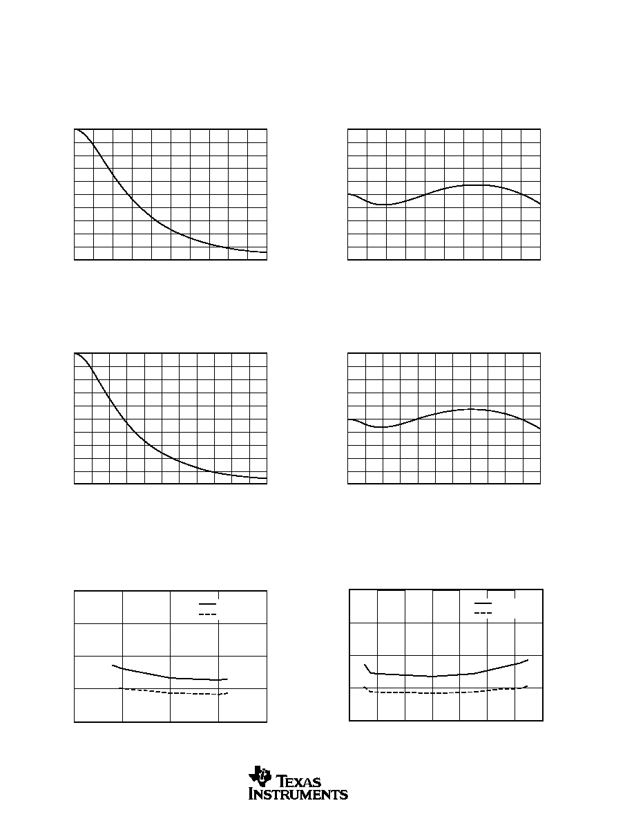
TYPICAL PERFORMANCE CURVES
All specifications at T
A
= +25 C, V
DD
= +3.3V, V
CC
= +5V, SCKI = 256f
S
(f
S
= 44.1kHz), and 24-bit input data, unless otherwise noted.
DIGITAL FILTER
Digital Filter (De-Emphasis Off, f
S
= 44.1kHz)
De-Emphasis Error
0
�20
�40
�60
�80
�100
�120
�140
�160
FREQUENCY RESPONSE (Sharp Roll-Off)
0
1
2
3
4
Frequency (x f
S
)
Amplitude (dB)
0.003
0.002
0.001
0
�0.001
�0.002
�0.003
PASSBAND RIPPLE (Sharp Roll-Off)
0
0.1
0.2
0.3
0.4
0.5
Frequency (x f
S
)
Amplitude (dB)
0.003
0.002
0.001
0
�0.001
�0.002
�0.003
PASSBAND RIPPLE (Sharp Roll-Off)
0
0.1
0.2
0.3
0.4
0.5
Frequency (x f
S
)
Amplitude (dB)
0
�20
�40
�60
�80
�100
�120
�140
FREQUENCY RESPONSE (Slow Roll-Off)
0
1
2
3
4
Frequency (x f
S
)
Amplitude (dB)
0
�2
�4
�6
�8
�10
�12
�14
�16
�18
�20
TRANSITION CHARACTERISTICS (Slow Roll-Off)
0
0.1
0.2
0.3
0.5
0.4
0.6
Frequency (x f
S
)
Amplitude (dB)
0.0
�1.0
�2.0
�3.0
�4.0
�5.0
�6.0
�7.0
�8.0
�9.0
�10.0
DE-EMPHASIS (f
S
= 32kHz)
0
2
4
6
8
10
12
14
Frequency (kHz)
Level (dB)
0.5
0.4
0.3
0.2
0.1
0.0
�0.1
�0.2
�0.3
�0.4
�0.5
DE-EMPHASIS ERROR (f
S
= 32kHz)
0
2
4
6
8
10
12
14
Frequency (kHz)
Error (dB)
0.5
0.4
0.3
0.2
0.1
0.0
�0.1
�0.2
�0.3
�0.4
�0.5
DE-EMPHASIS ERROR (f
S
= 32kHz)
0
2
4
6
8
10
12
14
Frequency (kHz)
Error (dB)
PCM1738
6
SBAS174B
TYPICAL PERFORMANCE CURVES
(Cont.)
All specifications at T
A
= +25 C, V
DD
= +3.3V, V
CC
= +5V, SCKI = 256f
S
(f
S
= 44.1kHz), and 24-bit input data, unless otherwise noted.
De-Emphasis Error
(Cont.)
ANALOG DYNAMIC PERFORMANCE
All specifications at T
A
= +25 C, V
DD
= +3.3V, V
CC
= +5V, SCKI = 256f
S
(f
S
= 44.1kHz), and 24-bit input data, unless otherwise noted.
Analog Dynamic Performance
0.0
�1.0
�2.0
�3.0
�4.0
�5.0
�6.0
�7.0
�8.0
�9.0
�10.0
DE-EMPHASIS (f
S
= 44.1kHz)
0
2
4
6
8
10
12
14
16
18
20
Frequency (kHz)
Level (dB)
0.5
0.4
0.3
0.2
0.1
0.0
�0.1
�0.2
�0.3
�0.4
�0.5
DE-EMPHASIS ERROR (f
S
= 44.1kHz)
0
2
4
6
8
10
12
14
16
18
20
Frequency (kHz)
Error (dB)
0.0
�1.0
�2.0
�3.0
�4.0
�5.0
�6.0
�7.0
�8.0
�9.0
�10.0
DE-EMPHASIS (f
S
= 48kHz)
0
2
4
6
8
10
12
14
16
18
22
Frequency (kHz)
Level (dB)
0.5
0.4
0.3
0.2
0.1
0.0
�0.1
�0.2
�0.3
�0.4
�0.5
DE-EMPHASIS ERROR (f
S
= 48kHz)
0
2
4
6
8
10
12
14
16
18
22
Frequency (kHz)
Error (dB)
0.0020
0.0015
0.0010
0.0005
0
THD+N/f
S
vs V
CC
4.50
4.75
5.00
5.25
5.50
V
CC
(V)
THD+N/f
S
(%)
44.1 kHz
96kHz
0.0020
0.0015
0.0010
0.0005
0
THD+N/f
S
vs TEMPERATURE
�40
�20
0
20
40
60
80
100
Temperature ( C)
THD+N/f
S
(%)
44.1 kHz
96kHz

PCM1738
7
SBAS174B
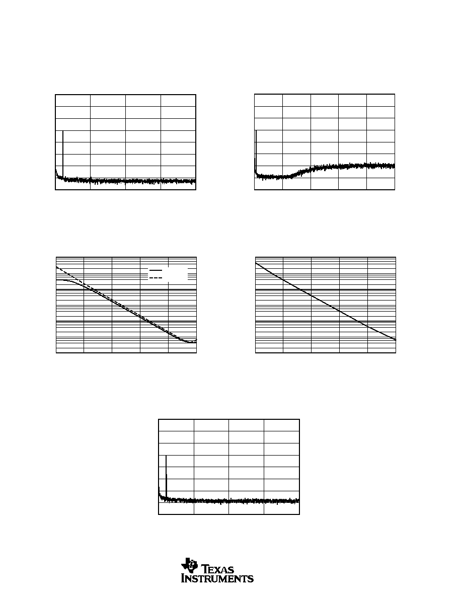
TYPICAL PERFORMANCE CURVES
(Cont.)
All specifications at T
A
= +25 C, V
DD
= +3.3V, V
CC
= +5V, SCKI = 256f
S
(f
S
= 44.1kHz), and 24-bit input data, unless otherwise noted.
Analog Dynamic Performance
(Cont.)
120
119
118
117
116
115
114
113
112
DYNAMIC RANGE vs V
CC
4.50
4.75
5.00
5.25
5.50
V
CC
(V)
Dynamic Range (dB)
44.1 kHz
96kHz
120
119
118
117
116
115
114
113
112
DYNAMIC RANGE vs TEMPERATURE
�40
�20
0
20
40
60
80
100
Temperature ( C)
Dynamic Range (dB)
44.1 kHz
96kHz
120
119
118
117
116
115
114
113
112
DYNAMIC RANGE vs TEMPERATURE
�40
�20
0
20
40
60
80
100
Temperature ( C)
Dynamic Range (dB)
44.1 kHz
96kHz
120
119
118
117
116
115
114
113
112
SIGNAL-TO-NOISE RATIO vs V
CC
4.50
4.75
5.00
5.25
5.50
V
CC
(V)
SNR (dB)
44.1 kHz
96kHz
120
119
118
117
116
115
114
113
112
SIGNAL-TO-NOISE RATIO vs TEMPERATURE
�40
�20
0
20
40
60
80
100
Temperature ( C)
SNR (dB)
44.1 kHz
96kHz
120
119
118
117
116
115
114
113
112
SIGNAL-TO-NOISE RATIO vs TEMPERATURE
�40
�20
0
20
40
60
80
100
Temperature ( C)
SNR (dB)
44.1 kHz
96kHz
118
117
116
115
114
113
112
111
110
CHANNEL SEPARATION vs V
CC
4.50
4.75
5.00
5.25
5.50
V
CC
(V)
Channel Separation (dB)
44.1 kHz
96kHz
118
117
116
115
114
113
112
111
110
CHANNEL SEPARATION vs TEMPERATURE
�40
�20
0
20
40
60
80
100
Temperature ( C)
Channel Separation (dB)
44.1 kHz
96kHz
118
117
116
115
114
113
112
111
110
CHANNEL SEPARATION vs TEMPERATURE
�40
�20
0
20
40
60
80
100
Temperature ( C)
Channel Separation (dB)
44.1 kHz
96kHz
PCM1738
8
SBAS174B
TYPICAL PERFORMANCE CURVES
(Cont.)
All specifications at T
A
= +25 C, V
DD
= +3.3V, V
CC
= +5V, SCKI = 256f
S
(f
S
= 44.1kHz), and 24-bit input data, unless otherwise noted.
Analog Dynamic Performance
(Cont.)
0
�20
�40
�60
�80
�100
�120
�140
�160
�60dB OUTPUT SPECTRUM (BW = 20kHz)
0
5k
10k
15k
20k
Frequency (Hz)
Output Level (dB)
0
�20
�40
�60
�80
�100
�120
�140
�160
�60dB OUTPUT SPECTRUM (BW = 100kHz)
0
20k
40k
60k
100k
80k
Frequency (Hz)
Output Level (dB)
100
10
1
0.1
0.01
0.001
0.0001
THD+N vs LEVEL (PCM MODE)
�100
�80
�60
�40
0
�20
Level ( ?)
THD+N (%)
44.1 kHz
96kHz
100
10
1
0.1
0.01
0.001
0.0001
THD+N vs LEVEL (DSD MODE)
�100
�80
�60
�40
0
�20
Level ( ?)
THD+N (%)
0
�20
�40
�60
�80
�100
�120
�140
�160
�60dB OUTPUT SPECTRUM ON DSD MODE
0
5k
10k
15k
20k
Frequency (Hz)
Output Level (dB)

PCM1738
9
SBAS174B
ANALOG FIR FILTER PERFORMANCE FOR DSD MODE
All specifications at T
A
= +25 C, V
DD
= +3.3V, V
CC
= +5V, SCKI = 11.2896MHz (44.1kHz � 256fS), and 50% modulation DSD data input, unless otherwise noted.
0
�1
�2
�3
�4
�5
�6
DSD FILTER 1
0
50
100
150
200
Frequency (kHz)
Gain (dB)
0
�20
�40
�60
�80
�100
DSD FILTER 1
0
500
1000
1500
Frequency (kHz)
Gain (dB)
0
�1
�2
�3
�4
�5
�6
DSD FILTER 2
0
50
100
150
200
Frequency (kHz)
Gain (dB)
0
�20
�40
�60
�80
�100
DSD FILTER 2
0
500
1000
1500
Frequency (kHz)
Gain (dB)
0
�1
�2
�3
�4
�5
�6
DSD FILTER 3
0
50
100
150
200
Frequency (kHz)
Gain (dB)
0
�20
�40
�60
�80
�100
DSD FILTER 3
0
500
1000
1500
Frequency (kHz)
Gain (dB)

PCM1738
10
SBAS174B
ANALOG FIR FILTER PERFORMANCE FOR DSD MODE
(Cont.)
All specifications at T
A
= +25 C, V
DD
= +3.3V, V
CC
= +5V, SCKI = 11.2896MHz (44.1kHz � 256fS), and 50% modulation DSD data input, unless otherwise noted.
0
�1
�2
�3
�4
�5
�6
DSD FILTER 4
0
50
100
150
200
Frequency (kHz)
Gain (dB)
0
�20
�40
�60
�80
�100
DSD FILTER 4
0
500
1000
1500
Frequency (kHz)
Gain (dB)
PCM1738
11
SBAS174B
SYSTEM CLOCK AND RESET
FUNCTIONS
SYSTEM CLOCK INPUT
The PCM1738 requires a system clock for operating the
digital interpolation filters and advanced segment DAC
modulators. The system clock is applied at the SCKI input
(pin 7). The PCM1738 has a system-clock detection circuit
that automatically senses if the system clock is operating at
128f
S
to 768f
S
. Table I shows examples of system-clock
frequencies for common audio sampling rates.
Figure 1 shows the timing requirements for the system clock
input. For optimal performance, it is important to use a clock
source with low phase jitter and noise. The PLL1700 multi-
clock generator is an excellent choice for providing the
PCM1738 system clock.
SYSTEM CLOCK OUTPUT
A buffered version of the system clock input is available at
the SCKO output (pin 10). SCKO can operate at either full
(f
SCKI
) or half (f
SCKI
/2) rate. The SCKO output frequency
may be programmed using the CLKD bit of Control Regis-
ter 19. The SCKO output pin can also be enabled or disabled
using the CLKE bit of Control Register 19. The default is
SCKO enabled.
POWER-ON AND EXTERNAL RESET FUNCTIONS
The PCM1738 includes a power-on reset function (see
Figure 2). The system clock input at SCKI should be active
for at least one clock period prior to V
DD
= 2.0V. With the
system clock active, and V
DD
> 2.0V, the power-on reset
function will be enabled. The initialization sequence re-
quires 1024 system clocks from the time V
DD
> 2.0V. After
the initialization period, the PCM1738 will be set to its reset
default state, as described in the Mode Control Register
section of this data sheet.
The PCM1738 also includes an external reset capability
using the RST input (pin 1). This allows an external control-
ler or master reset circuit to force the PCM1738 to initialize
to its reset default state.
See Figure 3 for external reset operation and timing. The
RST pin is set to a logic "0" for a minimum of 20ns. The
RST pin is then set to a logic "1" state that starts the
initialization sequence that requires 1024 system clock peri-
ods. After the initialization sequence is complete, the
PCM1738 will be set to its reset default state, as described
in the Mode Control Register section of this data sheet.
The external reset is especially useful in applications where
there is a delay between the PCM1738 power-up and system
clock activation. In this case, the RST pin should be held at
a logic "0" level until the system clock has been activated.
The RST pin may then be set to a logic "1" state to start the
initialization sequence.
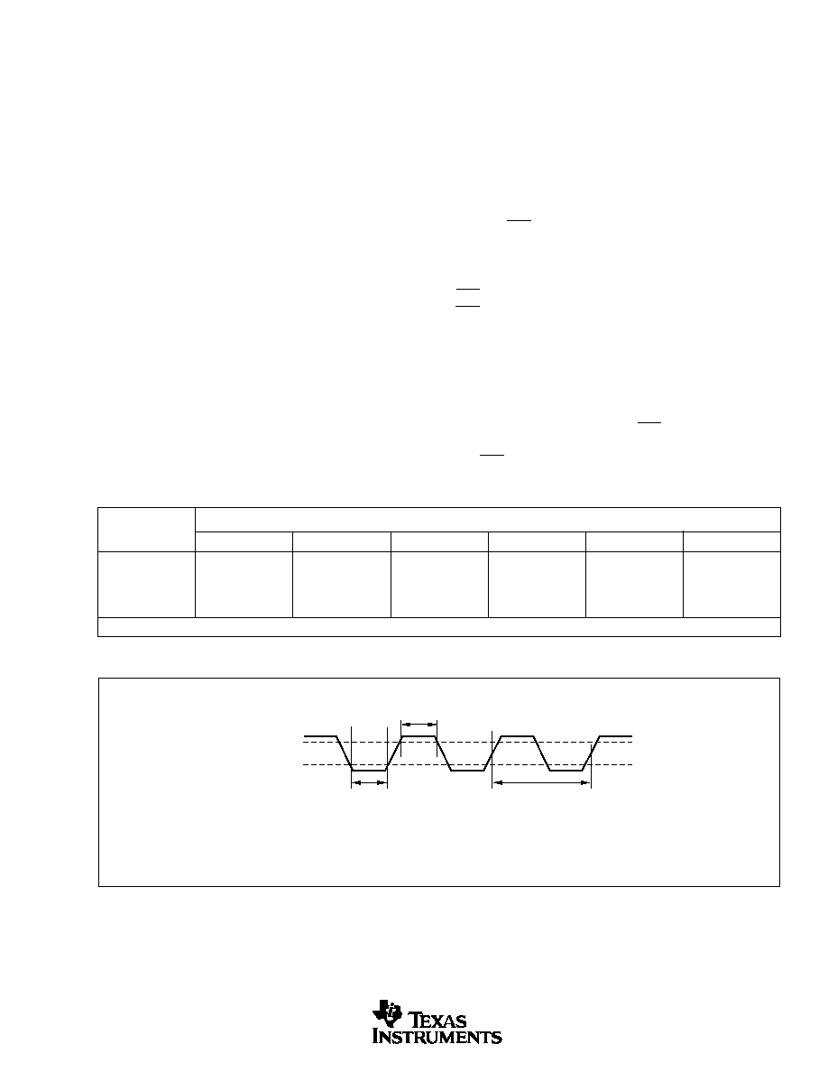
FIGURE 1. System Clock Input Timing.
SAMPLING
FREQUENCY
128f
S
192f
S
256f
S
384f
S
512f
S
768f
S
32kHz
4.0960
6.1440
8.1920
12.2880
16.3840
24.5760
44.1kHz
5.6488
8.4672
11.2896
16.9344
22.5792
33.8688
48kHz
6.1440
9.2160
12.2880
18.4320
24.5760
36.8640
96kHz
12.2880
18.4320
24.5760
36.8640
49.1520
73.7280
192kHz
24.5760
36.8640
49.1520
73.7280
See Note (1)
See Note (1)
NOTE: (1) This system clock is not supported for the given sampling frequency.
TABLE I. System Clock Rates for Common Audio Sampling Frequencies.
SYSTEM CLOCK FREQUENCY (f
SCLK
) (MHz)
t
SCKH
t
SCKL
2.0V
0.8V
System Clock
System clock pulse
cycle time
(1)
"H"
"L"
System Clock Pulse Width HIGH t
SCKH
: 5ns (min)
System Clock Pulse Width LOW t
SCKL
: 5ns (min)

PCM1738
12
SBAS174B
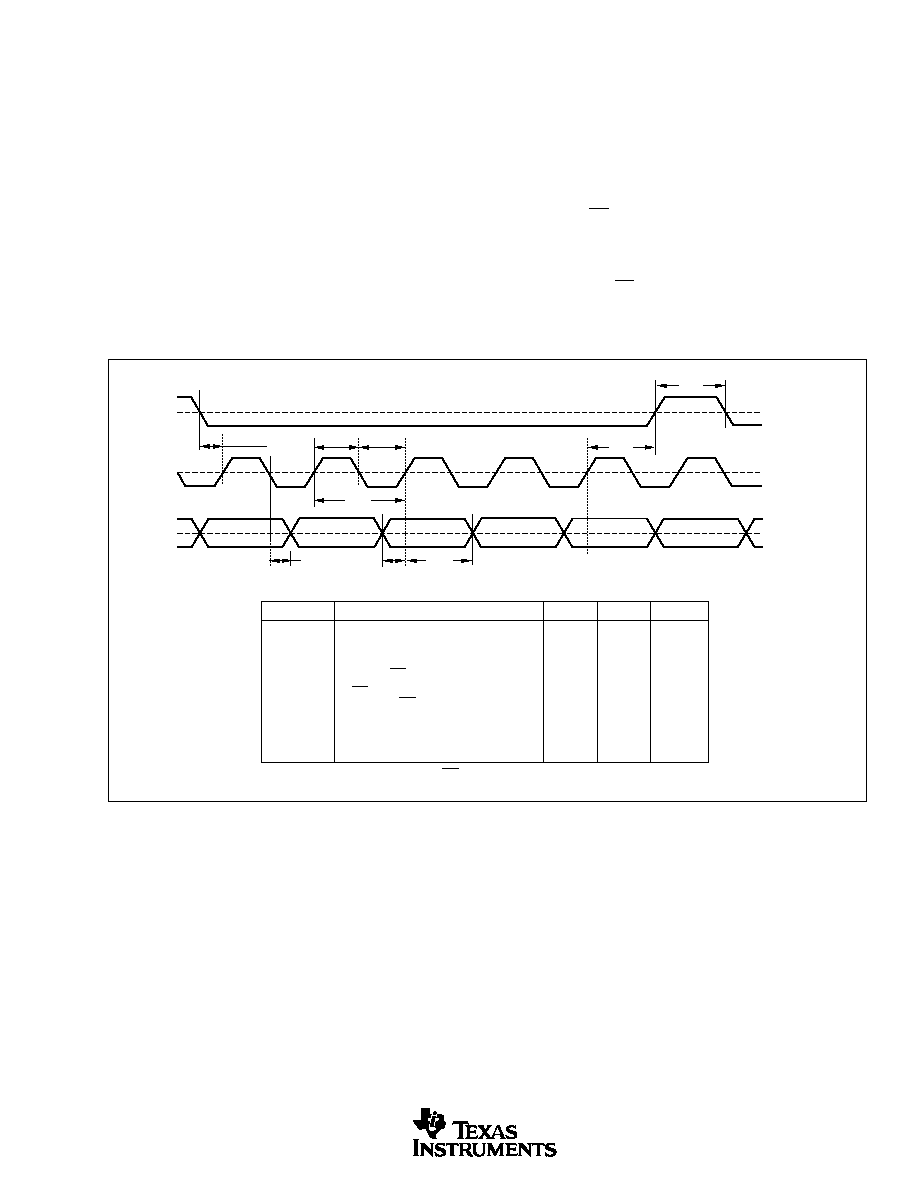
FIGURE 2. Power-On Reset Timing.
FIGURE 3. Audio Data Input Formats.
AUDIO DATA INTERFACE
AUDIO SERIAL INTERFACE
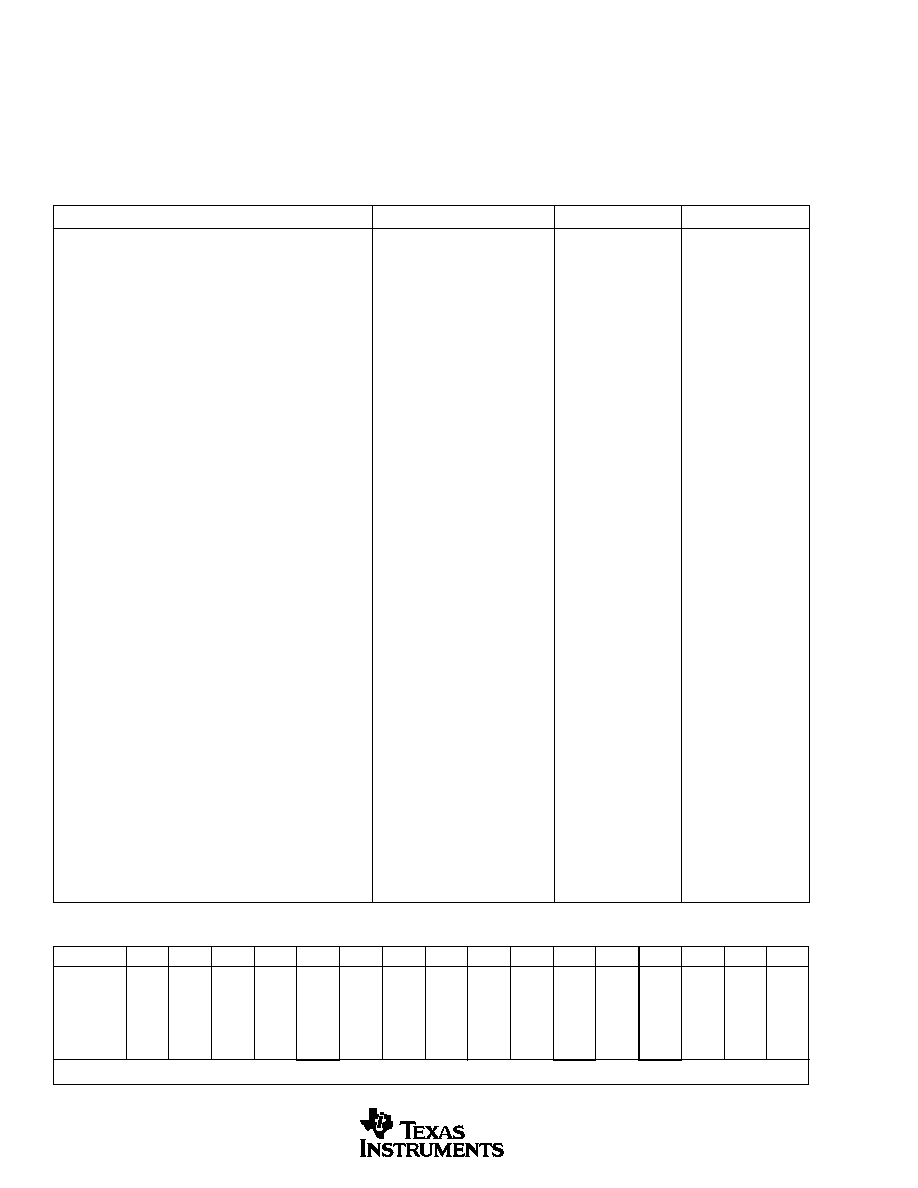
The audio serial interface for the PCM1738 is comprised of
a 3-wire synchronous serial port. It includes LRCK (pin 4),
BCK (pin 6), and DATA (pin 5). BCK is the serial audio bit
clock, used to clock the serial data present on DATA into the
audio interface's serial shift register. Serial data is clocked
into the PCM1738 on the rising edge of BCK. LRCK is the
serial audio left/right word clock, used to latch serial data
into the serial audio interface's internal registers.
LRCK should be synchronous to the system clock. In the
event these clocks are not synchronized, the PCM1738 can
compensate for the phase difference internally. If the phase
difference between LRCK and SCKI is greater than six bit
clocks (BCK), the synchronization is performed internally.
While the synchronization is processing, the analog output is
forced to the bipolar zero level. The synchronization typi-
cally occurs in less than one cycle of LRCK.
Ideally, it is recommended that LRCK and BCK be derived
from the system clock input or output, SCKI or SCKO. The
left/right clock (LRCK) is operated at the sampling fre-
quency, f
S
.
AUDIO DATA FORMATS AND TIMING
The PCM1738 supports industry-standard audio data formats,
including Standard Right-Justified, I
2
S, and Left-Justified. The
data formats are shown in Figure 4. Data formats are selected
using the format bits, FMT [2:0], in Control Register 18. The
default data format is 16-bit Standard. All formats require
Binary Two's Complement, MSB-first audio data. Figure 5
shows a detailed timing diagram for the serial audio interface.
1024 System Clock Periods
Reset
Reset Removal
2.4V/max
2.0V/typ
1.6V/min
V
DD
Internal Reset
System Clock
1024 System Clocks
t
RST
Reset
Reset Removal
System Clock
Internal Reset
RST (pin 1)
50% of V
DD
Reset Pulse Width LOW
t
RST
20ns (min)

PCM1738
13
SBAS174B
FIGURE 4. Audio Data Input Formats.
Audio Data Word = 24 Bit
Audio Data Word = 24 Bit
(1) Standard Data Format (Right Justified): L-Channel = HIGH, R-Channel = LOW
1/f
S
L-Channel
R-Channel
LRCK
BCK
14 15 16
22 23 24
15 16
1
2
DATA
19 20
1
2
DATA
15 16
1
2
19 20
1
2
23 24
1
2
LSB
MSB
18 19 20
DATA
Audio Data Word = 20 Bit
LSB
MSB
23 24
1
2
LSB
MSB
Audio Data Word = 16 Bit
1/f
S
L-Channel
R-Channel
LRCK
BCK
DATA
(3) I
2
S Data Format: L-Channel = LOW, R-Channel = HIGH
(2) Left-Justified Data Format: L-Channel = HIGH, R-Channel = LOW
1/f
S
L-Channel
R-Channel
LRCK
BCK
2
1
1
2
24
1
2
24
LSB
MSB
LSB
MSB
Audio Data Word = 16 Bit
DATA
1
2
1
2
1
2
16
1
2
16
LSB
MSB
1
2
24
1
2
24
LSB
MSB
Audio Data Word = 24 Bit
DATA

PCM1738
14
SBAS174B
FIGURE 5. Audio Interface Timing.
SYMBOL
PARAMETER
MIN
UNITS
t
BCY
BCK Pulse Cycle Time
70
ns
t
BCL
BCK High Level Time
30
ns
t
BCH
BCK Low Level Time
30
ns
t
BL
BCK Rising Edge to LRCK Edge
10
ns
t
LB
LRCK Falling Edge to BCK Rising Edge
10
ns
t
DS
DATA Set Up Time
10
ns
t
DH
DATA Hold Time
10
ns
---
LRCK Clock Duty
50% 2-Bit Clock
LRCK
BCK
DATA
50% of V
DD
50% of V
DD
50% of V
DD
t
BCH
t
BCL
t
LB
t
BL
t
DS
t
DH
t
BCY
EXTERNAL DIGITAL FILTER
INTERFACE AND TIMING
The PCM1738 supports an external digital-filter interface
comprised of a 4-wire synchronous serial port that allows
the use of an external digital filter. External filters include
the DF1704 and DF1706 from Texas Instruments, the
Pacific Microsonics PMD200, or a programmable digital
signal processor.
The 4-wire interface includes WCK as the word clock, BCK as
the bit clock, DATAL as the L-channel data, and DATAR as
the R-channel data. The external digital-filter interface is se-
lected using the DFTH bit of Control Register 20, which
functions to bypass the internal digital-filter portion of the
PCM1738. The 4-wire serial port is assigned to WDCK (pin 4),
BCK (pin 6), DATAL (pin 5), and DATAR (pin 15).
FIGURE 6. Serial Control Format.
NOTE: B15 is used for the selection of Write or Read. Setting W/R = 0 indicates a Write, while W/R = 1 indicates a Read.
B14 to B8 are used for register address.
B7 to B0 are used for register data.
DSD (DIRECT STREAM DIGITAL) FORMAT
INTERFACE AND TIMING
The PCM1738 supports a DSD format interface operation
that includes out-of-band noise filtering using an internal
Analog FIR filter. For DSD operation, pin 7 is redefined as
BCK, which operates at 64 x 44.1kHz; pin 5 is redefined as
DATAL (left-channel audio data), and pin 15 becomes
DATAR (right-channel audio data). Pins 4 and 6 must be
forced LOW in DSD mode. This configuration allows for
direct interface to a DSD decoder for SACD applications.
Detailed information for the DSD mode is provided in the
DSD Mode Operation section of this data sheet.
A0
D7
D6
D5
D4
D3
D2
D1
D0
W/R
A6
A5
A4
A3
A2
A1
CS
MC
MDI
D7
high impedance
D6
D5
D4
D3
D2
D1
D0
MDO
When Read mode is instructed
PCM1738
15
SBAS174B
FUNCTIONAL DESCRIPTIONS
ZERO DETECT
When the PCM1738 detects that the audio input data in the
L-channel or R-channel is continuously zero for 1024f
S
, the
PCM1738 sets ZEROL (pin 2) or ZEROR (pin 3) to HIGH.
Setting the INZD bit of mode register 19 can set both analog
outputs to the bipolar zero level when the input data of both
channels are zero.
SOFT MUTE
The PCM1738 supports mute operation by both hardware
and software control. When MUTE (pin 15) is set to HIGH,
both analog outputs are turned to the bipolar zero level.
When the MUTE bit in mode register 18 is set to "1", both
analog outputs are also turned to the bipolar zero level. The
speed to turn to the bipolar zero level is set by the ATS0 and
ATS1 bits in mode register 19.
SERIAL CONTROL INTERFACE
The serial control interface is a 4-wire synchronous serial
port that operates asynchronously to the serial audio inter-
face and the system clock (SCKI). The serial control inter-
face is utilized to program the on-chip mode registers. The
control interface includes MDO (pin 11), MDI (pin 12), MC
(pin 13), and CS (pin 14). MDO is the serial data output,
used to read back the values of the mode registers; MDI is
the serial data input, used to program the mode registers;
MC is the serial bit clock, used to shift data in and out of the
control port; and CS is the mode control enable, used to
enable the internal mode register access. Figures 6 and 7
show the format and timing for the serial control interface.
SYMBOL
PARAMETER
MIN
MAX
UNITS
t
MCY
MC Pulse Cycle Time
100
ns
t
MCL
MC Low Level Time
40
ns
t
MCH
MC High Level Time
40
ns
t
MHH
CS High Level Time
80
ns
t
MLS
CS Falling Edge to MC Rising Edge
15
ns
t
MLH
CS Hold Time
(1)
15
ns
t
MDH
MDI Hold Time
15
ns
t
MDS
MDI Set-Up Time
15
ns
t
MOS
MC Falling Edge to MDO Stable
30
ns
FIGURE 7. Control Interface Timing.
NOTE: (1) MC rising edge for LSB to CS rising edge.
50% of V
DD
50% of V
DD
50% of V
DD
ML
MC
MD
t
MLS
t
MCH
t
MCY
t
MDS
t
MDH
t
MCL
t
MHH
t
MLH
LSB
t
MOS
PCM1738
16
SBAS174B
MODE CONTROL REGISTERS
User-Programmable Mode Controls
The PCM1738 includes a number of user-programmable
functions that are accessed via mode control registers. The
registers are programmed using the Serial Control Interface
that was previously discussed in this data sheet. Table II lists
the available mode control functions, along with their reset
default conditions and associated register index.
Register Map
The mode control register map is shown in Table III. Each
register includes a W/R bit that indicates whether a register
read (W/R = 1) or write (W/R = 0) operation is performed.
FUNCTION
DEFAULT
REGISTER
BIT
FUNCTIONS AVAILABLE FOR BOTH WRITE AND READ
Digital Attenuation Control
0dB
Register 16 for L-Channel
ATL[7:0]
0dB to �120dB in 0.5dB Steps
Register 17 for R-Channel
ATR[7:0]
Attenuation Load Control
Attenuation Disabled
18
ATLD
Disable, Enable
Attenuation Speed Selection
x1f
S
19
ATS[1:0]
x1f
S
, x1/2f
S
, x1/4f
S
, x1/8f
S
Soft Mute Control
Mute Disabled
18
MUTE
Mute Disable, Enable
Infinite Zero Mute Control
Disabled
19
INZD
Disable, Enable
Input Audio Data Format Selection
16-Bit Standard Format
18
FMT[2:0]
16-, 20-, 24-Bit Standard (Right Justified) Format
24-Bit MSB-First Left-Justified Format
16-, 24-Bit I
2
S Format
De-Emphasis Control
De-Emphasis Disabled
18
DME
Disable, Enable
Sampling Rate Selection for De-Emphasis
De-Emphasis Disabled
18
DMF[1:0]
Disable, 44.1kHz, 48kHz, 32kHz
Digital Filter Roll-Off Selection
Sharp Roll-Off
19
FLT
Sharp Roll-Off, Slow Roll-Off
Output Phase Reversal
Normal
19
REV
Normal. Reverse
DAC Operation Control
DAC Operation Enabled
19
OPE
Enable, Disabled
System Clock (SCKO) Output Control
Output Enabled
19
CLKE
Output Enable, Disable
System Clock (SCKO) Rate Control
SCKI
19
CLKD
SCKI, SCKI/2
System Reset Control
Normal Operation
20
SRST
Reset Operation, Normal Operation
Mode Register Reset Control
Normal Operation
20
MRST
Reset Operation, Normal Operation
Digital-Filter Bypass Control
DF Enabled
20
DFTH
DF Enable, DF Bypass
Delta-Sigma Oversampling Rate Selection
x64f
S
20
OS[1:0]
x64f
S
, x128f
S
, x32f
S
Delta-Sigma Order Selection
Third Order
20
DSOS
Third-Order, Fifth-Order
Monaural Mode Selection
Stereo
20
MONO
Stereo, Monaural
Channel Selection for Monaural Mode Data
L-Channel
20
CHSL
L-Channel, R-Channel
FUNCTIONS AVAILABLE ONLY FOR READ
Zero Detection Flag
Not Zero = 0
21
ZFGL for L-Channel
Not Zero, Zero Detected
Zero Detected = 1
21
ZFGR for R-Channel
TABLE II. User-Programmable Mode Controls.
TABLE III. Mode Control Register Map.
REGISTER
B15
B14
B13
B12
B11
B10
B9
B8
B7
B6
B5
B4
B3
B2
B1
B0
16
W/R
0
0
1
0
0
0
0
ATL7
ATL6
ATL5
ATL4
ATL3
ATL2
ATL1
ATL0
17
W/R
0
0
1
0
0
0
1
ATR7
ATR6
ATR5
ATR4
ATR3
ATR2
ATR1
ATR0
18
W/R
0
0
1
0
0
1
0
ATLD
FMT2
FMT1
FMT0
DMF1
DMF0
DME
MUTE
19
W/R
0
0
1
0
0
1
1
REV
ATS1
ATS0
OPE
CLKD
CLKE
FLT
INZD
20
W/R
0
0
1
0
1
0
0
DSOS
SRST
MRST
DFTH
MONO
CHSL
OS1
OS0
21
R
0
0
1
0
1
0
1
RSV
RSV
RSV
RSV
RSV
RSV
ZFGR
ZFGL
NOTE: (1) RSV in Register 21 is assigned for factory test operation.

PCM1738
17
SBAS174B
REGISTER DEFINITIONS
B15
B14
B13
B12
B11
B10
B9
B8
B7
B6
B5
B4
B3
B2
B1
B0
REGISTER 16
W/R
0
0
1
0
0
0
0
ATL7
ATL6
ATL5
ATL4
ATL3
ATL2
ATL1
ATL0
REGISTER 17
W/R
0
0
1
0
0
0
1
ATR7
ATR6
ATR5
ATR4
ATR3
ATR2
ATR1
ATR0
W/R
Read/Write Mode Select
When W/R = 0, a Write operation is performed.
When W/R = 1, a Read operation is performed.
Default Value: 0
ATL/R[7:0]
Digital Attenuation Level Setting
These bits are Read/Write.
Default Value: 1111 1111
B
Each DAC output has a digital attenuator associated with it. The attenuator may be set from 0db to �120dB,
in 0.5dB steps. Alternatively, the attenuator may be set to infinite attenuation (or mute).
The attenuation data for each channel can be set individually. However, the data load control (ATLD bit of
Control Register 18) is common to both attenuators. ATLD must be set to "1" in order to change an
attenuator's setting. The attenuation level may be set using the following formula:
Attenuation Level (dB) = 0.5dB � (ATL/R[7:0]DEC � 255)
Where: ATL/R[7:0]DEC = 0 through 255
For: ATL/R[7:0]DEC = 0 through 14, the attenuator is set to infinite attenuation.
The following table shows attenuator levels for various settings.
ATL/R[7:0]
Decimal Value
Attenuator Level Setting
1111 1111
B
255
0dB, No Attenuation (default)
1111 1110
B
254
�0.5dB
1111 1101
B
253
�1.0dB
�
�
�
�
�
�
0001 0000
B
16
119.5dB
0000 1111
B
15
120.0dB
0000 1110
B
14
Mute
�
�
�
�
�
�
0000 0000
B
0
Mute
B15
B14
B13
B12
B11
B10
B9
B8
B7
B6
B5
B4
B3
B2
B1
B0
REGISTER 18
W/R
0
0
1
0
0
1
0
ATLD
FMT2
FMT1
FMT0
DMF1
DMF0
DME
MUTE
W/R
Read/Write Mode Control
When W/R = 0, a Write operation is performed.
When W/R = 1, a Read operation is performed.
Default Value: 0
ATLD
Attenuation Load Control
This bit is Read/Write.
Default Value: 0
ATLD = 0
Attenuation Control Disabled (default)
ATLD = 1
Attenuation Control Enabled
The ATLD bit is used to enable loading of attenuation data set by Register 16 through 17. When ATLD = 0,
the attenuation settings remain at the previously programmed level, ignoring new data loaded to Register 16
through 17. When ATLD = 1, attenuation data written to Register 16 through 17 is loaded normally.

PCM1738
18
SBAS174B
REGISTER 18
(Cont.)
FMT[2:0]
Audio Interface Data Format
These bits are Read/Write.
Default Value: 000
For external Digital-Filter Interface Mode (DFTH Mode), this register is operated as shown in the External
Digital-Filter Mode section of this data sheet.
The FMT[2:0] bits are used to select the data format for the serial audio interface.
FMT[2:0]
Audio Data Format Selection
000
16-Bit Standard Format, Right-Justified Data (default)
001
20-Bit Standard Format, Right-Justified Data
010
24-Bit Standard Format, Right-Justified Data
011
24-Bit MSB-First, Left-Justified Format Data
100
16-Bit I
2
S Format Data
101
24-Bit I
2
S Format Data
110
Reserved
111
Reserved
DMF[1:0]
Sampling Frequency Selection for the De-Emphasis Function
These bits are Read/Write.
Default Value: 00
DMF[1:0]
De-Emphasis Same Rate Selection
00
Disabled (default)
01
48kHz
10
44.0kHz
11
32kHz
The DMF[1:0] bits are used to select the sampling frequency used for the Digital De-Emphasis function when
it is enabled by setting the DME bit. The De-Emphasis curves are shown in the Typical Performance Curves
section of this data sheet.
For DSD Mode, Analog FIR filter performance may be selected using this register. Filter response plots are
shown in the Typical Performance Curves section of this data sheet. The Register Map is shown in the DSD
Mode section of this data sheet.
DME
Digital De-Emphasis Control
This bit is Read/Write.
Default Value: 0
For DSD mode, DME must be set to 1.
DME = 0
De-Emphasis Disabled (default)
DME = 1
De-Emphasis Enabled
The DME bit is used to enable or disable the De-Emphasis function for both channels.
MUTE
Soft Mute Control
This bit is Read/Write.
Default Value: 0
MUTE = 0
MUTE Disabled (default)
MUTE = 1
MUTE Enabled
The MUTE bit is used to enable the Soft Mute function for both channels. The mute function is also available
through the MUTE control input (pin 15). Soft Mute is performed by using the 256 step attenuator, cycling
one step per time interval to � (Mute). The time interval is set by the rate select bit (ATS), located in
Register 19.

PCM1738
19
SBAS174B
B15
B14
B13
B12
B11
B10
B9
B8
B7
B6
B5
B4
B3
B2
B1
B0
REGISTER 19
W/R
0
0
1
0
0
1
1
REV
ATS1
ATS0
OPE
CLKD
CLKE
FLT
INZD
W/R
Read/Write Mode Control
When W/R = 0, a Write operation is performed.
When W/R = 1, a Read operation is performed.
Default Value: 0
REV
Output Phase Reversal
This bit is Read/Write.
Default Value: 0
REV = 0
Normal Output (default)
REV = 1
Inverted Output
The REV bit is used to invert the output phase for both the Left and Right channels.
ATS[1:0]
Attenuation Rate Select
This bit is Read/Write.
Default Value: 00
ATS[1:0]
Attenuation Rate Selection
00
LRCK (default)
01
1/2 Times of LRCK
10
1/4 Times of LRCK
11
1/8 Times of LRCK
The ATS[1:0] bits are used to select the rate at which the attenuator is decremented or incremented during level
transitions.
OPE
DAC Operation Control
This bit is Read/Write.
Default Value: 0
OPE = 0
DAC Operation Enabled (default)
OPE = 1
DAC Operation Disabled
The OPE bit is used to enable or disable the analog output for both channels. Disabling the analog outputs forces
them to the bipolar zero level (BPZ), ignoring the audio data input(s).
CLKD
SCKO Frequency Selection
This bit is Read/Write.
Default Value: 0
CLKD = 0
Full Rate, f
SCKO
= f
SCKI
(default)
CLKD = 1
Half Rate, f
SCKO
= f
SCKI
/2
The CLKD bit is used to determine the output frequency at the system clock output pin, SCKO.
CLKE
SCKO Frequency Enable
This bit is Read/Write.
Default Value: 0
CLKE = 0
SCKO Enabled (default)
CLKE = 1
SCKO Disabled
The CLKE bit is used to enable or disable the system clock output pin, SCKO.

PCM1738
20
SBAS174B
REGISTER 19
(Cont.)
FLT
Digital Filter Roll-Off Control
This bit is Read/Write.
Default Value: 0
FLT = 0
Sharp Roll-Off (default)
FLT = 1
Slow Roll-Off
The FLT bit allows the user to select the digital filter roll-off characteristics. The filter responses for these
selections are shown in the Typical Performance Curves section of this data sheet.
INZD
Infinite Zero Detect Mute Control
This bit is Read/Write.
Default Value: 0
INZD = 0
Infinite Zero Detect Mute Disabled (default)
INZD = 1
Infinite Zero Detect Mute Enabled
The INZD bit is used to enable or disable the Zero Detect Mute function. Setting INZD = 1 allows the analog
outputs to be set to the bipolar zero level when the PCM1738 detects zero data for both Left and Right channels
for 1024 sampling periods (or LRCK cycles).
B15
B14
B13
B12
B11
B10
B9
B8
B7
B6
B5
B4
B3
B2
B1
B0
REGISTER 20
W/R
0
0
1
0
1
0
0
DSOS
SRST
MRST
DFTH
MONO
CHSL
OS1
OS0
W/R
Read/Write Mode Control
When W/R = 0, a Write operation is performed.
When W/R = 1, a Read operation is performed.
Default Value: 0
DSOS
Delta-Sigma Order Selection
This bit is Read/Write.
Default Value: 0
DSOS = 0
Third-Order Modulation (default)
DSOS = 1
Fifth-Order Modulation
The DSOS bit is used to change the order of delta-sigma modulation. It is possible to modify out-of-band
noise characteristics when combined with the oversampling controls (OS0 and OS1).
SRST
System Reset Control
This bit is Read/Write.
Default Value: 0
SRST = 0
Normal Operation (default)
SRST = 1
System Reset Operation
The SRST bit is used to reset the PCM1738 to the initial system condition.
MRST
Mode-Register Reset Control
This bit is Read/Write.
Default Value: 0
MRST = 0
Normal Operation (default)
MRST = 1
Mode-Register Reset Operation
The MRST bit is used to set the mode registers to their default conditions.

PCM1738
21
SBAS174B
REGISTER 20
(Cont.)
DFTH
Digital Filter Bypass (or Through Mode) Control
This bit is Read/Write.
Default Value: 0
DFTH = 0
Digital Filter Enabled (default)
DFTH = 1
Digital Filter Bypassed for Either External Digital Filter or DSD Mode
The DFTH bit is used to enable or bypass the internal digital filter. This function is used when using the external
digital-filter interface or the DSD mode interface.
MONO
Monaural Mode Selection
This bit is Read/Write.
Default Value: 0
MONO = 0
Stereo Mode (default)
MONO = 1
Monaural Mode
The MONO function is used to change the operation mode from normal stereo mode to monaural mode. When
the monaural mode is selected, both DACs operate in balanced mode for the selected audio input data. Left and
Right channel data selection is set by the CHSL bit, as described below.
CHSL
Channel Selection for Monaural Mode
This bit is Read/Write.
Default Value: 0
This bit is available when MONO = 1.
CHSL = 0
L-Channel Selected (default)
CHSL = 1
R-Channel Selected
The CHSL bit is used to set the audio data selection for the monaural mode.
OS[1:0]
Delta-Sigma Oversampling Rate Selection
These bits are available for Read/Write.
Default Value: 00
For DSD mode, this register is used to select the speed of BCK (pin 7) for the Analog FIR filter.
OS[1:0]
Operation Speed Select
00
64x (default)
01
Reserved
10
128x
11
32x
The OS bits are used to change the oversampling ratio of the delta-sigma modulator. This function is useful when
considering the output low-pass filter design that can handle a wide range of sampling rates. As an example,
selecting 128x for f
S
= 44.1kHz, 64x for f
S
= 96kHz, and 32x for f
S
= 192kHz operation would require a low-
pass filter with a single cutoff frequency to accommodate all three sampling rates.

PCM1738
22
SBAS174B
B15
B14
B13
B12
B11
B10
B9
B8
B7
B6
B5
B4
B3
B2
B1
B0
REGISTER 21
W/R
0
0
1
0
1
0
1
RSV
RSV
RSV
RSV
RSV
RSV
ZFGR
ZFGL
W/R
Read/Write Mode Control
Only available to set 0 for Read back mode.
ZFGx
Zero Detection Flag
When x = L or R, corresponding to the DAC output channel.
These bits are Read only.
Default Value: 00
ZFGx = 0
Not ZERO
ZFGx = 1
ZERO Detected
When the PCM1738 detects that audio input data is continuously zero for 1024f
S
, the ZFGx bit is set to 1 for
the corresponding channel(s). Zero detect flags are also available at ZEROL (pin 2) and ZEROR (pin 3).
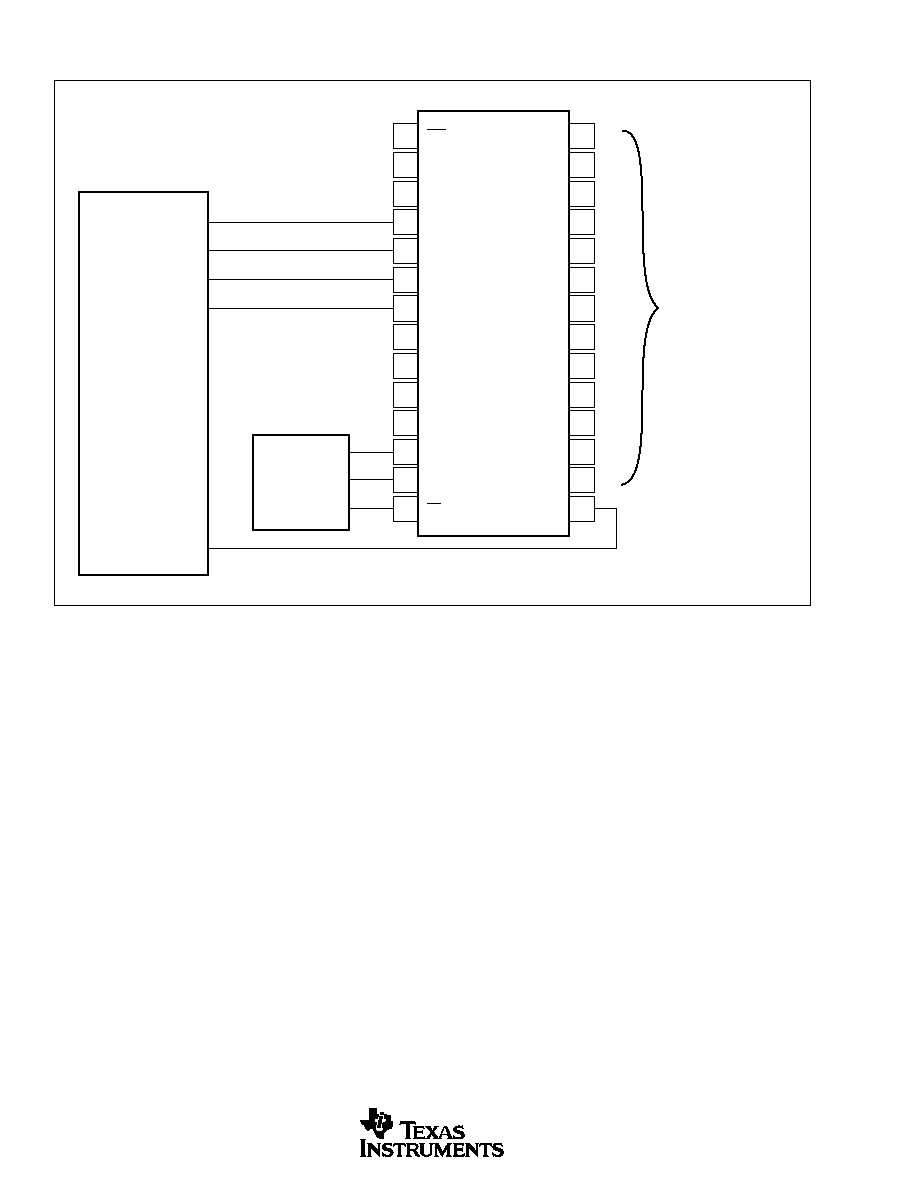
FIGURE 8. Typical Application Circuit for Standard PCM Audio Operation.
TYPICAL CONNECTION DIAGRAM IN PCM MODE
RST
ZEROL
ZEROR
LRCK
DATA
BCK
SCKI
DGND
V
DD
SCKO
MDO
MDI
MC
CS
V
CC
3
AGND2
I
OUT
L�
I
OUT
L+
V
CC
2
V
CC
1
V
COM
3
I
REF
V
COM
2
V
COM
1
AGND1
I
OUT
R+
I
OUT
R�
MUTE
1
2
3
4
5
6
7
8
9
10
11
12
13
14
28
27
26
25
24
23
22
21
20
19
18
17
16
15
PCM1738E
+
+
+
Analog Output Stage
Controller
+5.0V
+15V
�15V
V
OUT
L-Channel
V
OUT
R-Channel
L/R Clock (f
S
)
Audio DATA
Bit Clock
System Clock
+
+3.3V
+
-
+
-

PCM1738
23
SBAS174B
FIGURE 9. Typical Application for Analog Output Stage.
ANALOG OUTPUTS
Analog Gain by Balanced Amplifier
The I/V converters are followed by balanced amplifier
stages that sum the differential signals for each channel,
creating a single-ended voltage output. In addition, the
balanced amplifiers provide a second-order, low-pass filter
function that band limits the audio output signal. The cutoff
frequency and gain is given by external R and C component
values. In the case of Figure 9, the cutoff frequency is 45kHz
with a gain of 1. The output voltage for each channel is 6.2
Vp-p, or 2.2Vrms.
REFERENCE CURRENT RESISTOR
As shown in the analog output application circuit, marked
R
1
on Figure 9, there is a resistor connected from I
REF
(pin
21) to the analog ground, designated as R
1
. This resistor sets
the current for the internal reference circuit. The value of R
1
must be 16k , 1% in order to match the specified gain
error shown in the Specifications table.
ANALOG OUTPUT LEVEL AND I/V CONVERTER
The signal level of the DAC current output pins (I
OUT
L+,
I
OUT
L�, I
OUT
R+, and I
OUT
R�) is 2.48mA (p-p) at 0dB (Full
Scale). The voltage output of the I/V converter is given by
the following equation:
V
OUT
= 2.48mApp � R
F
(1)
Here, R
f
is the feedback resistor in the I/V (current-to-
voltage) conversion circuit, R
11
, R
12
, R
21
, and R
22
on a
typical application circuit. The common level of the I/V
conversion circuit must be the same as the common level of
DAC I
OUT
that is given by the V
COM
2 reference voltage,
+2.5V DC. The non-inverting inputs of the op amps shown
in the I/V circuits are connected to V
COM
2 to provide the
common bias voltage.
Op Amp for I/V Converter Circuit
The OPA627BP/BM, or 5534 type op amp, is recommended
for the I/V conversion circuit to obtain specified audio
performance. Dynamic performance, such as gain band-
width, settling time, and slew rate of the op amp creates
audio dynamic performance at the I/V section. Input noise
specification of the op amp should be considered to obtain
120dB S/N ratio.
V
CC
3
AGND2
I
OUT
L�
I
OUT
L+
V
CC
2
V
CC
1
V
COM
3
I
REF
V
COM
2
V
COM
1
AGND1
I
OUT
R+
I
OUT
R�
MUTE
28
27
26
25
24
23
22
21
20
19
18
17
16
15
PCM1738E
+
+
+
+5.0V
10 F
10 F
0.1 F
V
OUT
L-Channel
+
10 F
C
11
C
13
C
14
C
17
R
13
R
11
R
12
R
16
C
15
R
14
R
17
C
16
R
18
R
15
C
12
C
21
C
22
10 F
R
1
16k
V
OUT
R-Channel
C
23
C
24
C
27
R
23
R
21
R
22
R
26
C
25
R
24
R
27
C
26
R
28
R
25
OPA627BP, BM
or OPA5534 Op Amp
OPA134, OPA2134, or
OPA604, OPA2604 Op Amp
NOTE: Example R/C values for f
C
45kHz.
R
11
-R
18
, R
21
-R
28
: 620 , C
11
, C
12
, C
21
, C
22
: not populated, C
13
, C
14
,
C
23
, C
24
: 5600pF, C
15
, C
25
: 8200pF, C
16
, C
17
, C
26
, C
27
: 1800pF.
+
-
+
-
PCM1738
24
SBAS174B
FIGURE 10. Connection Diagram for External Digital Filter (Internal DF Bypass Mode) Application.
APPLICATION FOR EXTERNAL DIGITAL FILTER INTERFACE
APPLICATIONS FOR INTERFACING WITH THE
EXTERNAL DIGITAL FILTER PART
For some applications, it may be desirable to use an external
digital filter to perform the interpolation function, as it may
provide improved stopband attenuation or other special fea-
tures not available with the PCM1738's internal digital filter.
The PCM1738 supports the use of an external digital filter,
including:
� The DF1704 and DF1706 from Texas Instruments.
� Pacific Microsonics PMD100/200 HDCD Filter/Decoder ICs.
� Programmable Digital Signal Processors.
The external digital-filter application mode is available by
programming the following bits in the corresponding control
registers:
DFTH = 1 (Register 20)
DME = 0 (Register 18)
The pins used to provide the serial interface for the external
digital filter are shown in the application diagram of Figure 10.
The Word (WDCK) and Bit (BCK) clock signals, as well as
the audio data inputs (DATAL and DATAR) must be operated
at 8x or 4x the original sampling frequency at the input of the
digital filter.
SYSTEM CLOCK (SCKI) AND INTERFACE TIMING
The PCM1738, in external digital filter application, allows
any system-clock frequency synchronized with BCK and
WDCK. The system clock may be phase free with BCK and
WDCK. See Figure 17 for interface timing among WDCK,
BCK, DATAL, and DATAR.
AUDIO FORMAT
In external Digital-Filter Interface mode, the PCM1738
supports a right-justified audio format interface including
16-, 20-, and 24-bit audio data (see Figure 16) that should be
selected by FMT[2:0] of Control Register 18.
RST
ZEROL
ZEROR
WDCK
DATAL
BCK
SCKI
DGND
V
DD
SCKO
MDO
MDI
MC
CS
V
CC
3
AGND2
I
OUT
L�
I
OUT
L+
V
CC
2
V
CC
1
V
COM
3
I
REF
V
COM
2
V
COM
1
AGND1
I
OUT
R+
I
OUT
R�
DATAR
1
2
3
4
5
6
7
8
9
10
11
12
13
14
28
27
26
25
24
23
22
21
20
19
18
17
16
15
WDCK (Word Clock)
DATA-L
BCK
SCK
DATA-R
Mode
Control
DF1704
DF1706
PMD200
Analog
Output Stage
Same as Standard
Application

PCM1738
25
SBAS174B
FUNCTIONS AVAILABLE IN THE EXTERNAL DIGITAL-FILTER MODE
The external Digital-Filter mode allows access to the majority of the PCM1738's mode control functions. Table IV shows the
register mapping available when the external Digital-Filter mode is selected, along with descriptions of functions that are modified
for this mode selection.
TABLE IV. Register Mapping in the External Digital-Filter Mode.
REGISTER
B15
B14
B13
B12
B11
B10
B9
B8
B7
B6
B5
B4
B3
B2
B1
B0
16
W/R
0
0
1
0
0
0
0
�
�
�
�
�
�
�
�
17
W/R
0
0
1
0
0
0
1
�
�
�
�
�
�
�
�
18
W/R
0
0
1
0
0
1
0
�
FMT2
FMT1
FMT0
�
�
DME
(1)
�
19
W/R
0
0
1
0
0
1
1
�
�
�
OPE
CLKD
CLKE
�
INZD
20
W/R
0
0
1
0
1
0
0
RSV
SRST
MRST
DFTH
(1)
RSV
CHSL
OS1
OS0
21
R
0
0
1
0
1
0
1
RSV
RSV
RSV
RSV
RSV
RSV
ZFGR
ZFGL
NOTE: (1) This bit is required for selection of the external Digital-Filter mode. (2) "�" = function disabled.
FMT[2:0]
Audio Data Format Selection
These bits are available for Read/Write.
Default Value: 000
FMT[2:0]
Audio Data Format Select
000
16-Bit Right Justified Format (default)
001
20-Bit Right Justified Format
010
24-Bit Right Justified Format
Other
N/A
OS[1:0]
Delta-Sigma Oversampling Rate Selection
These bits are available for Read/Write.
Default Value: 00
OS[1:0]
Operation Speed Select
00
8x f
WCK
(default)
01
Reserved
10
16x f
WCK
11
4x f
WCK
The effective oversampling rate is determined by the oversampling performed by both the external digital filter
and the delta-sigma modulator. For example, if the external digital filter is 8x oversampling, and the user selects
OS[1:0] = 0, then the delta-sigma modulator will oversample by 8x, resulting in an effective oversampling rate
of 64x.
ZFGx
Zero Detection Flag
When x = L or R, corresponding to the DAC output channel.
These bits are available only for Read back.
Default Value: 00
ZFGx = 0
Not ZERO
ZFGx = 1
ZERO Detected
When the PCM1738 detects that audio input data is continuously zero for 1024f
S
, the ZFGx bit is set to 1 for
the corresponding channel(s). Zero detect flags are also available at ZEROL (pin 2) and ZEROR (pin 3).

PCM1738
26
SBAS174B
APPLICATION FOR DSD FORMAT (DSD MODE) INTERFACE
FEATURES
This mode is utilized for interfacing directly to a DSD
decoder, found in Super Audio CD (SACD) applications.
DSD Mode provides a low-pass filtering function to convert
the 1-bit oversampled data stream to the analog domain. The
filtering is provided using an Analog FIR filter structure.
Four FIR responses are available and may be selected via the
serial control interface. Refer to the Typical Performance
Curves section of this data sheet for Analog FIR plots. See
Figures 1 and 2 for interface timing and specification, and
Figures 17 and 18 for timing and interface specification in
DSD mode.
PIN ASSIGNMENT WHEN IN DSD
FORMAT INTERFACE
Several pins are redefined for DSD Mode operation. These
include:
� DATA (Pin 5)
DATAL, L-Channel DSD Data Input
� MUTE (Pin 15) DATAR, R-Channel DSD Data Input
� SCKI (Pin 7) Bit Clock (BCK) for DSD Data (64 x 44.1kHz)
� LRCK (Pin 4) Set LOW
� BCK (Pin 6) Set LOW
Typical connection to a DSD decoder is shown in Figure 11.
FIGURE 11. Connection Diagram for DSD Format Interface.
RST
ZEROL
ZEROR
N/A
DATAL
N/A
BCK
DGND
V
DD
SCKO
MDO
MDI
MC
CS
V
CC
3
AGND2
I
OUT
L�
I
OUT
L+
V
CC
2
V
CC
1
V
COM
3
I
REF
V
COM
2
V
COM
1
AGND1
I
OUT
R+
I
OUT
R�
DATAR
1
2
3
4
5
6
7
8
9
10
11
12
13
14
28
27
26
25
24
23
22
21
20
19
18
17
16
15
DATA-L
Bit Clock (n � f
S
)
DATA-R
Mode
Control
DSD Decoder
Always Set LOW
Always Set LOW
Analog
Output Stage
Same as Standard
Application
PCM1738
27
SBAS174B
DSD MODE CONFIGURATION AND FUNCTION CONTROLS
Configuration for DSD Interface mode:
� DFTH = 1 (Register 20)
� DME = 1 (Register 18)
Table V shows the register mapping available in DSD Mode.
TABLE V. Register Mapping in DSD Mode.
REGISTER
B15
B14
B13
B12
B11
B10
B9
B8
B7
B6
B5
B4
B3
B2
B1
B0
16
W/R
0
0
1
0
0
0
0
�
�
�
�
�
�
�
�
17
W/R
0
0
1
0
0
0
1
�
�
�
�
�
�
�
�
18
W/R
0
0
1
0
0
1
0
�
�
�
�
DMF1
DMF0
DME
(1)
�
19
W/R
0
0
1
0
0
1
1
�
�
�
OPE
CLKD
CLKE
�
�
20
W/R
0
0
1
0
1
0
0
RSV
SRST
MRST
DFTH
(1)
RSV
RSV
OS1
OS0
21
R
0
0
1
0
1
0
1
RSV
RSV
RSV
RSV
RSV
RSV
�
�
NOTE: (1) This bit is required for selection of the external Digital Filter mode. (2) "�" = function disabled.
DMF[1:0]
Analog FIR Performance Selection
These bits are available for Read/Write.
Default Value: 00
DMF[1:0]
Analog FIR Performance Select
00
DSD Filter 1
01
DSD Filter 2
10
DSD Filter 3
11
DSD Filter 4
Plots for the four Analog FIR filter responses are shown in the Typical Performance Curves of this data sheet.
OS[1:0]
Analog FIR Operation Speed Select Selection
These bits are available for Read/Write.
Default Value: 00
OS[1:0]
Operation Speed Select
00
f
SCKI
(default)
01
Reserved
10
Reserved
11
f
SCKI
/2
The OS bit in the DSD mode is used to select the operating rate of analog FIR.
REQUIREMENTS FOR SYSTEM CLOCK
The bit clock (BCK) for DSD Mode is required at pin 7 of the PCM1738. The frequency of the bit clock may be N times of
the sampling frequency. Generally, N is 64 in DSD application.
The interface timing between the bit clock, DATAL, and DATAR is required to meet the same setup and hold time
specifications as shown for the PCM Audio format interface in Figure 5.

PCM1738
28
SBAS174B
APPLICATION FOR MONAURAL MODE OPERATION
FIGURE 12. Connection Diagram for Monaural-Mode Interface.
L/R Clock
Audio Data
Bit Clock
System Clock
Controller
PCM1738
PCM1738
Analog Output
Stage
Analog Output
Stage
V
OUT
L-Channel
V
OUT
R-Channel
LRCK
DATA
BCK
SCKI
MC, CS, MDI
I
OUT
L�
I
OUT
L+
I
OUT
R�
I
OUT
R+
I
OUT
L�
I
OUT
L+
I
OUT
R�
I
OUT
R+
LRCK
DATA
BCK
SCKI
MC, CS, MDI
Single-channel signals within stereo-audio data input is
output to both I
OUT
L and I
OUT
R as differential outputs.
Selection of channels to output is available with the CHSL
bit in Register 20. Applications, such as monaural operation,
are useful for high-end audio applications to provide over
120dB for dynamic range. A typical MONO mode applica-
tion is shown in Figure 12.

PCM1738
29
SBAS174B
FIGURE 13. Architecture of Advanced Segment DAC.
+
Advanced
DWA
Analog
Output
ICOB
Decoder
3rd-Order,
5th-Level,
Current
Segment
DAC
0 � 62
Level
0 � 66
0 � 4
Level
Upper
6 Bits
MSB and
Lower 18 Bits
Digital
Input
24-Bit
8f
S
The PCM1738 utilizes the newly developed Advanced Seg-
ment DAC architecture to achieve excellent dynamic perfor-
mance and improved tolerance to clock jitter. The PCM1738
provides balanced current outputs, allowing the user to
optimize analog performance externally. The structure of the
Advanced Segment DAC architecture is shown in Figure 13.
Digital input data from the digital interpolation filter is split
into six upper bits and 18 lower bits. The upper six bits are
converted to ICOB (Inverted Complementary Offset Binary)
code. The lower 18 bits associated with the MSB are
processed by fifth-level, third-order, delta-sigma modulators
operated at 64f
S
by default conditions. The first level of the
modulator is equivalent to 1LSB of the above code con-
verter. The data groups processed in the ICOB converter and
the third-order delta-sigma modulator are summed together
to create up to 67 levels of digital code that is then processed
by the DWA (Data Weighted Averaging) to reduce noise
produced by element mismatch. The output data from the
DWA block is then converted to an analog output using a
differential current segment DAC.
To learn more details regarding the Advanced Segment
DAC architecture, please refer to the paper presented at the
109
th
AES Convention entitled "A 117db, D-Range, Cur-
rent-mode, Multi-Bit, Audio DAC for PCM and DSD Audio
Playback" by Nakao, Terasawa, Aoyagi, Terada, and
Hamasaki of Burr-Brown Japan (now part of Texas Instru-
ments).
THEORY OF OPERATION
ADVANCED SEGMENT DAC
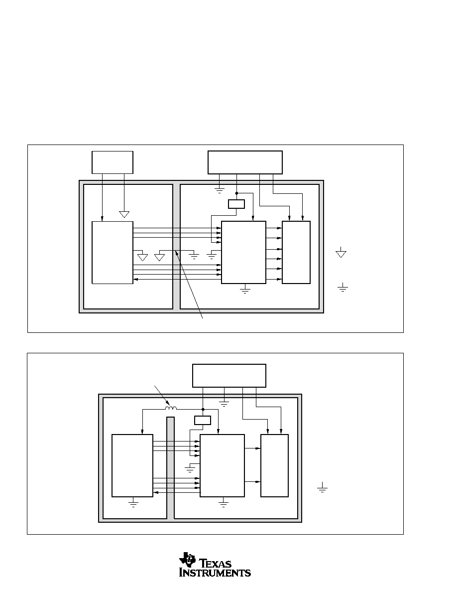
PCM1738
30
SBAS174B
CONSIDERATIONS FOR
APPLICATIONS CIRCUITS
PCB LAYOUT GUIDELINES
A typical PCB floor plan for the PCM1738 is shown in
Figure 14. A ground plane is recommended, with the analog
and digital sections being isolated from one another using a
split or cut in the circuit board. The PCM1738 should be
oriented with the digital I/O pins facing the ground plane
split/cut to allow for short, direct connections to the digital
audio interface and control signals originating from the
digital section of the board.
Separate power supplies are recommended for the digital
and analog sections of the board. This prevents the switching
noise present on the digital supply from contaminating the
analog power supply and degrading the dynamic perfor-
mance of the DACs. In cases where a common +5V supply
must be used for the analog and digital sections, an induc-
tance (RF choke, ferrite bead) should be placed between the
analog and digital +5V supply connections to avoid coupling
of the digital switching noise into the analog circuitry.
Figure 15 shows the recommended approach for single-
supply applications.
FIGURE 14. Recommended PCB Layout.
PCM1738
V
CC
V
DD
DGND
Return Path for Digital Signals
Analog
Ground
Digital
Ground
AGND
Output
Circuits
DIGITAL SECTION
ANALOG SECTION
Digital Logic
and
Audio
Processor
Digital Power
+V
D
DGND
Analog Power
+5VA
+V
S
AGND
REG
�V
S
FIGURE 15. Single-Supply PCB Layout.
PCM1738
V
CC
V
DD
DGND
Output
Circuits
RF Choke or Ferrite Bead
Common
Ground
AGND
DIGITAL SECTION
ANALOG SECTION
V
DD
Power Supplies
+5V
+V
S
AGND
REG
�V
S
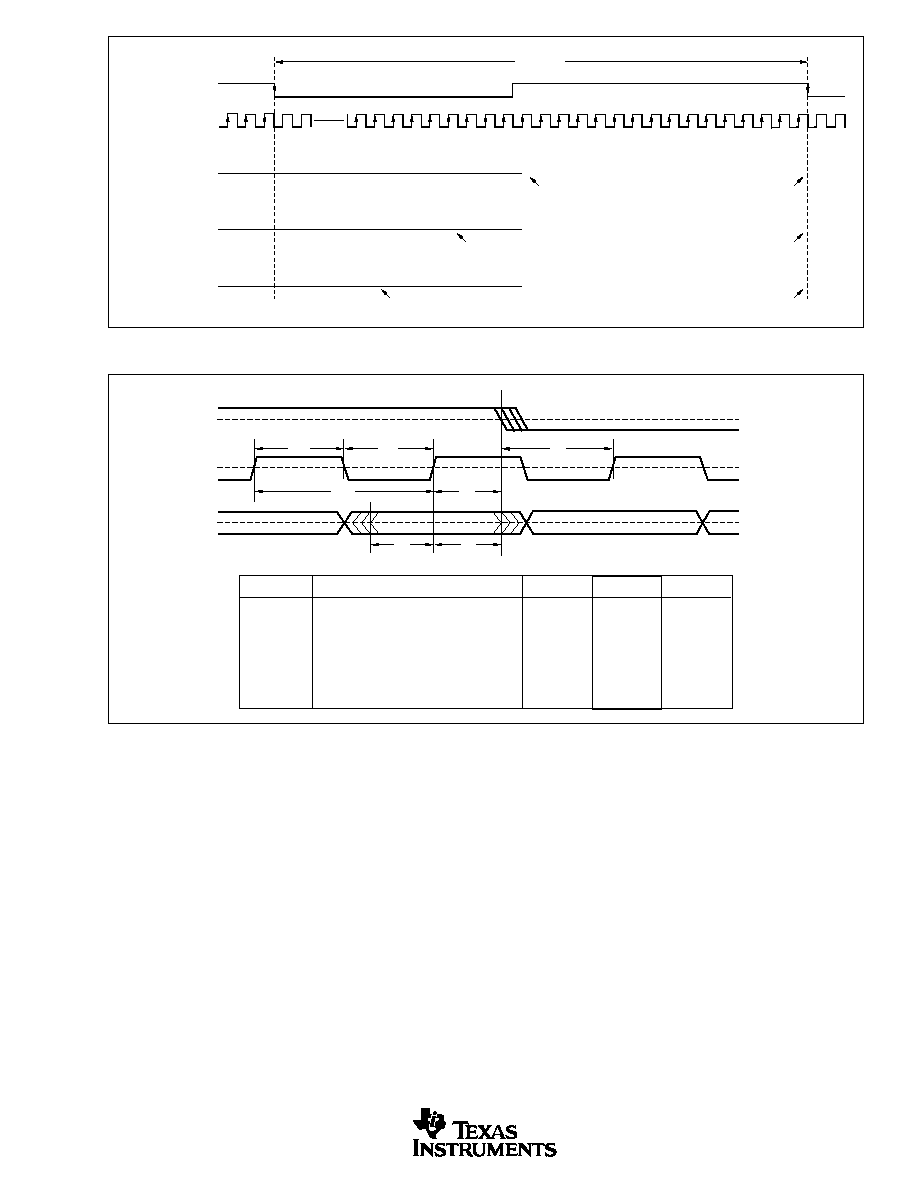
PCM1738
31
SBAS174B
BYPASS AND DECOUPLING CAPACITOR
REQUIREMENTS
Various sized decoupling capacitors can be used, with no
special tolerances being required. All capacitors should be
located as close as physically possible to the power supply
and reference pins of the PCM1738 to reduce noise pickup
from surrounding circuitry. Aluminum electrolytic capaci-
tors that are designed for hi-fi audio applications are recom-
mended for larger values, while metal-film or monolithic
ceramic capacitors are recommended for smaller values.
I/V SECTION
I/V conversion, using the circuit shown in Figure 9, achieves
data-sheet performance (see Figure 9). To obtain 0.0005%
THD+N, 117dB signal-to-noise ratio audio performance, THD+N
and input noise performance an op amp IC must be considered.
Input noise of the op amp directly effects the output noise level
of the application.
All components of the I/V section should be located physi-
cally close to the PCM1738 current outputs. All connections
should be made as short as possible to eliminate pickup of
radiated noise.
POST LOW-PASS FILTER DESIGN
The out-of-band noise level and sampling spectrum level are
much lower than typical delta-sigma type DACs, due to the
combination of a high-performance digital filer and the
advanced segment DAC architecture. The use of a second-
or third-order filter is recommended for the post low-pass
filter (see Figure 9 for a second-order filter) following the I/
V conversion stage. The cutoff frequency of the post LPF is
dependent upon the application, given the variety of sam-
pling rates supported by the CD-DA, DVD-M, DVD-A, and
SACD systems.
FIGURE 16. Audio Data Input Format for External Digital Filter (Internal DF Bypass Mode) Application.
15
16
1
2
11
12
13
14
15
16
3
4
5
6
7
8
9
10
WDCK
BCK
DATAL
DATAR
MSB
LSB
Audio Data Word = 16 Bit
19
20
5
6
15
16
17
18
19
20
7
8
1
2
3
4
9
10
11
12
13
14
DATAL
DATAR
MSB
LSB
Audio Data Word = 20 Bit
23
24
9
10
19
20
21
22
23
24
11
12
13
14
15
16
1
2
3
4
5
6
7
8
17
18
DATAL
DATAR
MSB
LSB
Audio Data Word = 24 Bit
1/4f
S
or 1/8f
S
FIGURE 17. Audio Interface Timing for External Digital Filter (Internal DF Bypass Mode) Application.
SYMBOL
PARAMETER
MIN
MAX
UNITS
t
BCY
BCK Pulse Cycle Time
18
ns
t
BCL
BCK Pulse Width LOW
7
ns
t
BCH
BCK Pulse Width HIGH
7
ns
t
BL
BCK Rising Edge to WDCK Falling Edge
5
ns
t
LB
WDCK Falling Edge to BCKIN Rising Edge
5
n
s
t
DS
DATA Set-Up Time
5
ns
t
DH
DATA Hold Time
5
ns
WDCK
BCK
DATAL
DATAR
50% of V
DD
50% of V
DD
50% of V
DD
t
BCH
t
BCL
t
LB
t
BL
t
DS
t
DH
t
BCY

PACKAGING INFORMATION
Orderable Device
Status
(1)
Package
Type
Package
Drawing
Pins Package
Qty
Eco Plan
(2)
Lead/Ball Finish
MSL Peak Temp
(3)
PCM1738E
ACTIVE
SSOP
DB
28
47
None
CU SNPB
Level-1-235C-UNLIM
PCM1738E/2K
ACTIVE
SSOP
DB
28
2000
None
CU SNPB
Level-1-235C-UNLIM
(1)
The marketing status values are defined as follows:
ACTIVE: Product device recommended for new designs.
LIFEBUY: TI has announced that the device will be discontinued, and a lifetime-buy period is in effect.
NRND: Not recommended for new designs. Device is in production to support existing customers, but TI does not recommend using this part in
a new design.
PREVIEW: Device has been announced but is not in production. Samples may or may not be available.
OBSOLETE: TI has discontinued the production of the device.
(2)
Eco Plan - May not be currently available - please check
http://www.ti.com/productcontent
for the latest availability information and additional
product content details.
None: Not yet available Lead (Pb-Free).
Pb-Free (RoHS): TI's terms "Lead-Free" or "Pb-Free" mean semiconductor products that are compatible with the current RoHS requirements
for all 6 substances, including the requirement that lead not exceed 0.1% by weight in homogeneous materials. Where designed to be soldered
at high temperatures, TI Pb-Free products are suitable for use in specified lead-free processes.
Green (RoHS & no Sb/Br): TI defines "Green" to mean "Pb-Free" and in addition, uses package materials that do not contain halogens,
including bromine (Br) or antimony (Sb) above 0.1% of total product weight.
(3)
MSL, Peak Temp. -- The Moisture Sensitivity Level rating according to the JEDECindustry standard classifications, and peak solder
temperature.
Important Information and Disclaimer:The information provided on this page represents TI's knowledge and belief as of the date that it is
provided. TI bases its knowledge and belief on information provided by third parties, and makes no representation or warranty as to the
accuracy of such information. Efforts are underway to better integrate information from third parties. TI has taken and continues to take
reasonable steps to provide representative and accurate information but may not have conducted destructive testing or chemical analysis on
incoming materials and chemicals. TI and TI suppliers consider certain information to be proprietary, and thus CAS numbers and other limited
information may not be available for release.
In no event shall TI's liability arising out of such information exceed the total purchase price of the TI part(s) at issue in this document sold by TI
to Customer on an annual basis.
PACKAGE OPTION ADDENDUM
www.ti.com
9-Dec-2004
Addendum-Page 1

IMPORTANT NOTICE
Texas Instruments Incorporated and its subsidiaries (TI) reserve the right to make corrections, modifications,
enhancements, improvements, and other changes to its products and services at any time and to discontinue
any product or service without notice. Customers should obtain the latest relevant information before placing
orders and should verify that such information is current and complete. All products are sold subject to TI's terms
and conditions of sale supplied at the time of order acknowledgment.
TI warrants performance of its hardware products to the specifications applicable at the time of sale in
accordance with TI's standard warranty. Testing and other quality control techniques are used to the extent TI
deems necessary to support this warranty. Except where mandated by government requirements, testing of all
parameters of each product is not necessarily performed.
TI assumes no liability for applications assistance or customer product design. Customers are responsible for
their products and applications using TI components. To minimize the risks associated with customer products
and applications, customers should provide adequate design and operating safeguards.
TI does not warrant or represent that any license, either express or implied, is granted under any TI patent right,
copyright, mask work right, or other TI intellectual property right relating to any combination, machine, or process
in which TI products or services are used. Information published by TI regarding third-party products or services
does not constitute a license from TI to use such products or services or a warranty or endorsement thereof.
Use of such information may require a license from a third party under the patents or other intellectual property
of the third party, or a license from TI under the patents or other intellectual property of TI.
Reproduction of information in TI data books or data sheets is permissible only if reproduction is without
alteration and is accompanied by all associated warranties, conditions, limitations, and notices. Reproduction
of this information with alteration is an unfair and deceptive business practice. TI is not responsible or liable for
such altered documentation.
Resale of TI products or services with statements different from or beyond the parameters stated by TI for that
product or service voids all express and any implied warranties for the associated TI product or service and
is an unfair and deceptive business practice. TI is not responsible or liable for any such statements.
Following are URLs where you can obtain information on other Texas Instruments products and application
solutions:
Products
Applications
Amplifiers
amplifier.ti.com
Audio
www.ti.com/audio
Data Converters
dataconverter.ti.com
Automotive
www.ti.com/automotive
DSP
dsp.ti.com
Broadband
www.ti.com/broadband
Interface
interface.ti.com
Digital Control
www.ti.com/digitalcontrol
Logic
logic.ti.com
Military
www.ti.com/military
Power Mgmt
power.ti.com
Optical Networking
www.ti.com/opticalnetwork
Microcontrollers
microcontroller.ti.com
Security
www.ti.com/security
Telephony
www.ti.com/telephony
Video & Imaging
www.ti.com/video
Wireless
www.ti.com/wireless
Mailing Address:
Texas Instruments
Post Office Box 655303 Dallas, Texas 75265
Copyright
2004, Texas Instruments Incorporated