 | –≠–ª–µ–∫—Ç—Ä–æ–Ω–Ω—ã–π –∫–æ–º–ø–æ–Ω–µ–Ω—Ç: PCM1773PW | –°–∫–∞—á–∞—Ç—å:  PDF PDF  ZIP ZIP |
PCM1772
PCM1773
SLES010D ≠ SEPTEMBER 2001 ≠ REVISED MAY 2004
LOW VOLTAGE AND LOW POWER STEREO AUDIO
DIGITAL TO ANALOG CONVERTER WITH LINEOUT AMPLIFIER
FEATURES
D
Multilevel DAC Including Lineout Amplifier
D
Analog Performance (V
CC1
, V
CC2
= 2.4 V):
- Dynamic Range: 98 dB Typ
- THD+N at 0 dB: 0.007% Typ
D
1.6-V to 3.6-V Single Power Supply
D
Low Power Dissipation: 6 mW at V
CC1
,
V
CC2
= 2.4 V
D
System Clock: 128 f
S
, 192 f
S
, 256 f
S
, 384 f
S
D
Sampling Frequency: 5 kHz to 50 kHz
D
Software Control (PCM1772):
- 16-, 20-, 24-Bit Word Available
- Left-, Right-Justified, and I
2
S
- Slave/Master Selectable
- Digital Attenuation: 0 dB to
≠
62 dB,
1 dB/Step
- 44.1-kHz Digital De-Emphasis
- Zero Cross Attenuation
- Digital Soft Mute
- Monaural Analog-In With Mixing
- Monaural Speaker Mode
D
Hardware Control (PCM1773):
- Left-Justified and I
2
S
- 44.1-kHz Digital De-Emphasis
- Monaural Analog-In With Mixing
D
Pop-Noise-Free Circuit
D
3.3-V Tolerant
D
Packages: TSSOP-16 and VQFN-20, Lead Free
APPLICATIONS
D
Portable Audio Player
D
Cellular Phone
D
PDA
D
Other Applications Requiring Low-Voltage
Operation
DESCRIPTION
The PCM1772 and PCM1773 devices are CMOS,
monolithic, integrated circuits which include stereo
digital-to-analog converters, lineout circuitry, and
support circuitry in small TSSOP-16 and VQFN-20
packages.
The data converters use TI's enhanced multilevel
-
architecture, which employs noise shaping and
multilevel amplitude quantization to achieve excellent
dynamic performance and improved tolerance to clock
jitter. The PCM1772 and PCM1773 devices accept
several industry standard audio data formats with 16- to
24-bit data, left-justified, I
2
S, etc., providing easy
interfacing to audio DSP and decoder devices.
Sampling rates up to 50 kHz are supported. A full set of
user-programmable functions are accessible through a
3-wire serial control port, which supports register write
functions.
PRODUCTION DATA information is current as of publication date. Products
conform to specifications per the terms of Texas Instruments standard warranty.
Production processing does not necessarily include testing of all parameters.
Please be aware that an important notice concerning availability, standard warranty, and use in critical applications of Texas Instruments
semiconductor products and disclaimers thereto appears at the end of this data sheet.
Burr Brown Products
from Texas Instruments
Copyright
2004, Texas Instruments Incorporated

PCM1772
PCM1773
SLES010D ≠ SEPTEMBER 2001 ≠ REVISED MAY 2004
www.ti.com
2
These devices have limited built-in ESD protection. The leads should be shorted together or the device placed in conductive foam during
storage or handling to prevent electrostatic damage to the MOS gates.
PACKAGE/ORDERING INFORMATION
PRODUCT
PACKAGE
PACKAGE
PACKAGE
CODE
OPERATION
TEMPERATURE
RANGE
PACKAGE
MARKING
ORDERING
NUMBER
TRANSPORT
MEDIA
PCM1772PW
16-lead TSSOP
16PW
≠25
∞
C to 85
∞
C
PCM1772
PCM1772PW
Tube
PCM1772PW
16-lead TSSOP
16PW
≠25
∞
C to 85
∞
C
PCM1772
PCM1772PWR
Tape and reel
PCM1772RGA
20-lead VQFN
20RGA
≠25
∞
C to 85
∞
C
PCM1772
PCM1772RGA
Tray
PCM1772RGA
20-lead VQFN
20RGA
≠25
∞
C to 85
∞
C
PCM1772
PCM1772RGAR
Tape and reel
PCM1773PW
16-lead TSSOP
16PW
≠25
∞
C to 85
∞
C
PCM1773
PCM1773PW
Tube
PCM1773PW
16-lead TSSOP
16PW
≠25
∞
C to 85
∞
C
PCM1773
PCM1773PWR
Tape and reel
PCM1773RGA
20-lead VQFN
20RGA
≠25
∞
C to 85
∞
C
PCM1773
PCM1773RGA
Tray
PCM1773RGA
20-lead VQFN
20RGA
≠25
∞
C to 85
∞
C
PCM1773
PCM1773RGAR
Tape and reel
ABSOLUTE MAXIMUM RATINGS
over operating free-air temperature range unless otherwise noted(1)
PCM1772
PCM1773
Supply voltage: VCC1, VCC2
4 V
Supply voltage differences: VCC1, VCC2
±
0.1 V
Ground voltage differences
±
0.1 V
Digital input voltage
≠0.3 V to 4 V
Input current (any terminals except supplies)
±
10 mA
Operating temperature
≠40
∞
C to 125
∞
C
Storage temperature
≠55
∞
C to 150
∞
C
Junction temperature
150
∞
C
Lead temperature (soldering)
260
∞
C, 5 s
Package temperature (IR reflow, peak)
260
∞
C
(1) Stresses beyond those listed under "absolute maximum ratings" may cause permanent damage to the device. These are stress ratings only, and
functional operation of the device at these or any other conditions beyond those indicated under "recommended operating conditions" is not
implied. Exposure to absolute-maximum-rated conditions for extended periods may affect device reliability.
PCM1772
PCM1773
SLES010D ≠ SEPTEMBER 2001 ≠ REVISED MAY 2004
www.ti.com
3
ELECTRICAL CHARACTERISTICS
all specifications at TA = 25
∞
C, VCC1 = VCC2 = 2.4 V, fS = 44.1 kHz, system clock = 256 fS and 24-bit data, RL = 10 k
, unless otherwise noted
PARAMETER
TEST CONDITIONS
PCM1772PW, PCM1773PW,
PCM1772RGA, PCM1773RGA
UNIT
PARAMETER
TEST CONDITIONS
MIN
TYP
MAX
UNIT
Resolution
24
Bits
OPERATING FREQUENCY
Sampling frequency (fS)
5
50
kHz
System clock frequency
128 fS, 192 fS, 256 fS, 384 fS
DIGITAL INPUT/OUTPUT(1)(2)
VIH
Input logic level
0.7 VCC1
Vdc
VIL
Input logic level
0.3 VCC1
Vdc
IIH
Input logic current
VIN = VCC1
10
µ
A
IIL
Input logic current
VIN = 0 V
≠10
µ
A
VOH
Output logic level(3)
IOH = ≠2 mA
0.7 VCC1
Vdc
VOL
Output logic level(3)
IOL = 2 mA
0.3 VCC1
Vdc
DYNAMIC PERFORMANCE (LINE OUTPUT)
Full scale output voltage
0 dB
0.75 VCC2
VP-P
Dynamic range
EIAJ, A-weighted
90
98
dB
Signal-to-noise ratio
EIAJ, A-weighted
90
98
dB
THD+N
0 dB
0.007%
0.015%
Channel separation
70
80
dB
Load resistance
10
k
DC ACCURACY
Gain error
±
2
±
8
% of FSR
Gain mismatch, channel-to-channel
±
2
±
8
% of FSR
Bipolar zero error
VOUT = 0.5 VCC1 at BPZ
±
30
±
75
mV
ANALOG LINE INPUT (MIXING CIRCUIT)
Analog input voltage range
0.584 VCC2
VP-P
Gain (analog input to line output)
0.91
Analog input impedance
10
k
THD+N
AIN = 0.56 VCC2 (peak-to-peak)
0.1%
DIGITAL FILTER PERFORMANCE
Pass band
0.454 fS
Stop band
0.546 fS
Pass-band ripple
±
0.04
dB
Stop-band attenuation
≠50
dB
Group delay
20/fS
44.1-kHz de-emphasis error
±
0.1
dB
ANALOG FILTER PERFORMANCE
Frequency response
at 20 kHz
±
0.2
dB
(1) Digital inputs and outputs are CMOS compatible.
(2) All logic inputs are 3.3-V tolerant and not terminated internally.
(3) LRCK and BCK terminals

PCM1772
PCM1773
SLES010D ≠ SEPTEMBER 2001 ≠ REVISED MAY 2004
www.ti.com
4
ELECTRICAL CHARACTERISTICS (continued)
all specifications at TA = 25
∞
C, VCC1 = VCC2 = 2.4 V, fS = 44.1 kHz, system clock = 256 fS and 24-bit data, RL = 10 k
, unless otherwise noted
PARAMETER
TEST CONDITIONS
PCM1772PW, PCM1773PW,
PCM1772RGA, PCM1773RGA
UNIT
PARAMETER
TEST CONDITIONS
MIN
TYP
MAX
UNIT
POWER SUPPLY REQUIREMENTS
Voltage range, VCC1, VCC2
1.6
2.4
3.6
Vdc
ICC1
BPZ input
1.5
2.5
mA
ICC2
Supply current
BPZ input
1
2.5
mA
ICC1 +
ICC2
Supply current
Power down(4)
5
15
µ
A
Power dissipation
BPZ input
6
12
mW
Power dissipation
Power down(4)
12
36
µ
W
TEMPERATURE RANGE
Operation temperature
≠25
85
∞
C
JA
Thermal resistance
PCM1772PW, -73PW: 16-terminal
TSSOP
150
∞
C/W
JA
Thermal resistance
PCM1772RGA, -73RGA: 20-terminal
VQFN
130
∞
C/W
(4) All input signals are held static.
PIN ASSIGNMENTS
1
2
3
4
5
6
7
8
16
15
14
13
12
11
10
9
LRCK
DATA
BCK
PD
AGND1
AGND2
V
COM
V
OUT
R
SCKI
MS
MC
MD
V
CC1
V
CC2
AIN
V
OUT
L
PCM1772
PW PACKAGE
(TOP VIEW)
1
2
3
4
5
6
7
8
16
15
14
13
12
11
10
9
LRCK
DATA
BCK
PD
AGND1
AGND2
V
COM
V
OUT
R
SCKI
FMT
AMIX
DEMP
V
CC1
V
CC2
AIN
V
OUT
L
PCM1773
PW PACKAGE
(TOP VIEW)
PCM1772
RGA PACKAGE
(TOP VIEW)
DATA
BCK
PD
AGND1
AGND2
LRCK
NC
NC
NC
SCKI
COM
NC
AIN
V
R
OUT
V
L
OUT
V
NC ≠ No internal connection
FMT
AMIX
DEMP
VCC1
VCC2
PCM1773
RGA PACKAGE
(TOP VIEW)
DATA
BCK
PD
AGND1
AGND2
LRCK
NC
NC
NC
SCKI
COM
NC
AIN
V
MS
MC
MD
V
CC1
V
CC2
1
2
3
4
5
15
14
13
12
11
6
7
8
9 10
20 19 18 17 16
1
2
3
4
5
15
14
13
12
11
6
7
8
9 10
20 19 18 17 16
R
OUT
V
L
OUT
V
PCM1772
PCM1773
SLES010D ≠ SEPTEMBER 2001 ≠ REVISED MAY 2004
www.ti.com
5
Terminal Functions
PCM1772PW
TERMINAL
I/O
DESCRIPTIONS
NAME
NO.
I/O
DESCRIPTIONS
AGND1
5
--
Analog ground. This is a return for VCC1.
AGND2
6
--
Analog ground. This is a return for VCC2.
AIN
10
I
Monaural analog signal mixer input. The signal can be mixed with the output of L- and R-channel DACs.
BCK
3
I/O
Serial bit clock. Clocks the individual bits of the audio data input, DATA. In the slave interface mode, this clock is input
from external device. In master interface mode, the PCM1772 device generates the BCK output to an external device.
DATA
2
I
Serial audio data input
LRCK
1
I/O
Left and right clock. Determines which channel is being input on the audio data input, DATA. The frequency of LRCK
must be the same as the audio sampling rate. In the slave interface mode, this clock is input from an external device.
In the master interface mode, the PCM1772 device generates the LRCK output to an external device.
MC
14
I
Mode control port serial bit clock input. Clocks the individual bits of the control data input, MD.
MD
13
I
Mode control port serial data input. Controls the operation mode on the PCM1772 device.
MS
15
I
Mode control port select. The control port is active when this terminal is low.
PD
4
I
Reset input. When low, the PCM1772 device is powered down, and all mode control registers are reset to default
settings.
SCKI
16
I
System clock input
VCC1
12
--
Power supply for all analog circuits except the lineout amplifier.
VCC2
11
--
Analog power supply for the lineout amplifier circuits. The voltage level must be the same as VCC1.
VCOM
7
--
Decoupling capacitor connection. An external 10-
µ
F capacitor connected from this terminal to analog ground is
required for noise filtering. Voltage level of this terminal is 0.5 VCC2 nominal.
VOUTL
9
O
L-channel analog signal output of the lineout amplifiers
VOUTR
8
O
R-channel analog signal output of the lineout amplifiers
PCM1772RGA
TERMINAL
I/O
DESCRIPTIONS
NAME
NO.
I/O
DESCRIPTIONS
AGND1
4
--
Analog ground. This is a return for VCC1.
AGND2
5
--
Analog ground. This is a return for VCC2.
AIN
10
I
Monaural analog signal mixer input. The signal can be mixed with output of L- and R-channel DACs.
BCK
2
I/O
Serial bit clock. Clocks the individual bits of the audio data input, DATA. In the slave interface mode, this clock is input
from an external device. In the master interface mode, the PCM1772 device generates the BCK output to an external
device.
DATA
1
I
Serial audio data input
LRCK
20
I/O
Left and right clock. Determines which channel is being input on the audio data input, DATA. The frequency of LRCK
must be the same as the audio sampling rate. In the slave interface mode, this clock is input from an external device.
In the master interface mode, the PCM1772 device generates the LRCK output to an external device.
MC
14
I
Mode control port serial bit clock input. Clocks the individual bits of the control data input, MD.
MD
13
I
Mode control port serial data input. Controls the operation mode on the PCM1772 device.
MS
15
I
Mode control port select. The control port is active when this terminal is low.
NC
8, 17,
18, 19
--
No connect
PD
3
I
Reset input. When low, the PCM1772 device is powered down, and all mode control registers are reset to default
settings.
SCKI
16
I
System clock input
VCC1
12
--
Power supply for all analog circuits except lineout amplifier.
VCC2
11
--
Analog power supply for lineout amplifier circuits. The voltage level must be the same as VCC1.
VCOM
6
--
Decoupling capacitor connection. An external 10-
µ
F capacitor connected from this terminal to analog ground is
required for noise filtering. Voltage level of this terminal is 0.5 VCC2 nominal.
VOUTR
7
O
R-channel analog signal output of lineout amplifiers.
VOUTL
9
O
L-channel analog signal output of lineout amplifiers.

PCM1772
PCM1773
SLES010D ≠ SEPTEMBER 2001 ≠ REVISED MAY 2004
www.ti.com
6
Terminal Functions
PCM1773PW
TERMINAL
I/O
DESCRIPTIONS
NAME
NO.
I/O
DESCRIPTIONS
AGND1
5
--
Analog ground. This is a return for VCC1.
AGND2
6
--
Analog ground. This is a return for VCC2.
AIN
10
--
Monaural analog signal mixer input. The signal can be mixed with the output of L- and R-channel DACs.
AMIX
14
I
Analog mixing control
BCK
3
I
Serial bit clock. Clocks the individual bits of the audio data input, DATA.
DATA
2
I
Serial audio data input
DEMP
13
I
De-emphasis control
FMT
15
I
Data format select
LRCK
1
I
Left and right clock. Determines which channel is being input on the audio data input, DATA. The frequency of LRCK
must be the same as the audio sampling rate.
PD
4
I
Reset input. When low, the PCM1773 device is powered down, and all mode control registers are reset to default
settings.
SCKI
16
I
System clock input
VCC1
12
--
Power supply for all analog circuits except the lineout amplifier
VCC2
11
--
Analog power supply for the lineout amplifier circuits. The voltage level must be the same as VCC1.
VCOM
7
--
Decoupling capacitor connection. An external 10-
µ
F capacitor connected from this terminal to analog ground is
required for noise filtering. Voltage level of this terminal is 0.5 VCC2 nominal.
VOUTL
9
O
L-channel analog signal output of the lineout amplifiers
VOUTR
8
O
R-channel analog signal output of the lineout amplifiers
PCM1773RGA
TERMINAL
I/O
DESCRIPTIONS
NAME
NO.
I/O
DESCRIPTIONS
AGND1
4
--
Analog ground. This is a return for VCC1.
AGND2
5
--
Analog ground. This is a return for VCC2.
AIN
10
--
Monaural analog signal mixer input. The signal can be mixed with output of L- and R-channel DACs.
AMIX
14
I
Analog mixing control
BCK
2
I
Serial bit clock. Clocks the individual bits of the audio data input, DATA.
DATA
1
I
Serial audio data input
DEMP
13
I
De-emphasis control
FMT
15
I
Data format select
LRCK
20
I
Left and right clock. Determines which channel is being input on the audio data input, DATA. The frequency of LRCK
must be the same as the audio sampling rate.
NC
8, 17,
18, 19
--
No connect
PD
3
I
Reset input. When low, the PCM1773 device is powered down, and all mode control registers are reset to default
settings.
SCKI
16
I
System clock input
VCC1
12
--
Power supply for all analog circuits except the lineout amplifier
VCC2
11
--
Analog power supply for the lineout amplifier circuits. The voltage level must be the same as VCC1.
VCOM
6
--
Decoupling capacitor connection. An external 10-
µ
F capacitor connected from this terminal to analog ground is
required for noise filtering. Voltage level of this terminal is 0.5 VCC2 nominal.
VOUTL
9
O
L-channel analog signal output of the lineout amplifiers
VOUTR
7
O
R-channel analog signal output of the lineout amplifiers

PCM1772
PCM1773
SLES010D ≠ SEPTEMBER 2001 ≠ REVISED MAY 2004
www.ti.com
7
FUNCTIONAL BLOCK DIAGRAM
DAC
Audio
Interface
◊
8
Digital
Filter
+
DAC
SPI
Port
◊
8
Digital
Filter
+
VCOM
Clock Manager
Power Supply
LRCK
DATA
BCK
(FMT) MS
(AMIX) MC
(DEMP) MD
SCKI
PD
VCC1
VCC2
VOUTR
VCOM
VOUTL
AIN
Digital
Attenuator
Lineout
Amplifier
( ) : PCM1773
AGND1
AGND2
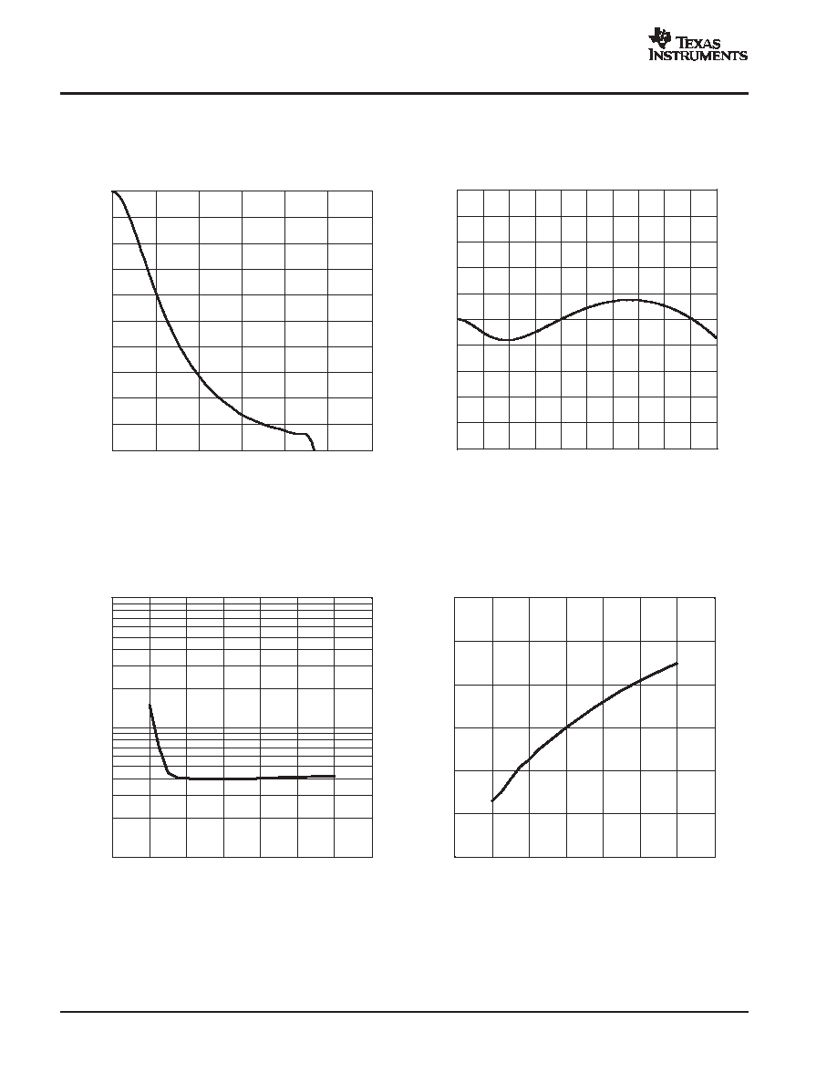
TYPICAL PERFORMANCE CURVES
DIGITAL FILTER
Digital Filter (De-Emphasis Off)
Figure 1
f ≠ Frequency [
fS]
-140
-120
-100
-80
-60
-40
-20
0
0
1
2
3
4
Amplitude ≠ dB
AMPLITUDE
vs
FREQUENCY
Figure 2
f ≠ Frequency [
fS]
-0.05
-0.04
-0.03
-0.02
-0.01
0.00
0.01
0.02
0.03
0.04
0.05
0.0
0.1
0.2
0.3
0.4
0.5
Amplitude ≠ dB
AMPLITUDE
vs
FREQUENCY
All specifications at TA = 25
∞
C, VCC1 = VCC2 = 2.4 V, fS = 44.1 kHz, system clock = 256 fS and 24-bit data, RL = 10 k
, unless otherwise noted.
PCM1772
PCM1773
SLES010D ≠ SEPTEMBER 2001 ≠ REVISED MAY 2004
www.ti.com
8
De-Emphasis Curves
Figure 3
f ≠ Frequency ≠ kHz
-10
-9
-8
-7
-6
-5
-4
-3
-2
-1
0
0.0
0.1
0.2
0.3
0.4
0.5
0.6
De-Emphasis Level ≠ dB
DE-EMPHASIS LEVEL
vs
FREQUENCY
Figure 4
f ≠ Frequency ≠ kHz
-0.5
-0.4
-0.3
-0.2
-0.1
-0.0
0.1
0.2
0.3
0.4
0.5
0
2
4
6
8
10
12
14
16
18
20
DE-EMPHASIS ERROR
vs
FREQUENCY
De-Emphasis Error ≠ dB
0.0
Figure 5
0.01
0.10
1.00
1.2
1.6
2.0
2.4
2.8
3.2
3.6
4.0
VCC ≠ Supply Voltage ≠ V
THD+N ≠ T
otal Harmonic Distortion + Noise ≠ %
TOTAL HARMONIC DISTORTION + NOISE
vs
SUPPLY VOLTAGE
0.1
0.01
0.001
Figure 6
VCC ≠ Supply Voltage ≠ V
92
94
96
98
100
102
104
1.2
1.6
2.0
2.4
2.8
3.2
3.6
4.0
Dynamic Range ≠ dB
DYNAMIC RANGE
vs
SUPPLY VOLTAGE
All specifications at TA = 25
∞
C, VCC1 = VCC2 = 2.4 V, fS = 44.1 kHz, system clock = 256 fS and 24-bit data, RL = 10 k
, unless otherwise noted.

PCM1772
PCM1773
SLES010D ≠ SEPTEMBER 2001 ≠ REVISED MAY 2004
www.ti.com
9
Figure 7
VCC ≠ Supply Voltage ≠ V
92
94
96
98
100
102
104
1.2
1.6
2.0
2.4
2.8
3.2
3.6
4.0
SNR ≠ dB
SNR
vs
SUPPLY VOLTAGE
Figure 8
VCC ≠ Supply Voltage ≠ V
74
76
78
80
82
84
86
1.2
1.6
2.0
2.4
2.8
3.2
3.6
4.0
Channel Separation ≠ dB
CHANNEL SEPARATION
vs
SUPPLY VOLTAGE
Figure 9
0.01
0.10
1.00
-40
-20
0
20
40
60
80
100
TA ≠ Free-Air Temperature ≠
∞
C
THD+N ≠ T
otal Harmonic Distortion + Noise ≠ %
TOTAL HARMONIC DISTORTION + NOISE
vs
FREE-AIR TEMPERATURE
0.1
0.01
0.001
Figure 10
TA ≠ Free-Air Temperature ≠
∞
C
94
95
96
97
98
99
100
101
102
-40
-20
0
20
40
60
80
100
Dynamic Range ≠ dB
DYNAMIC RANGE
vs
FREE-AIR TEMPERATURE
All specifications at TA = 25
∞
C, VCC1 = VCC2 = 2.4 V, fS = 44.1 kHz, system clock = 256 fS and 24-bit data, RL = 10 k
, unless otherwise noted.

PCM1772
PCM1773
SLES010D ≠ SEPTEMBER 2001 ≠ REVISED MAY 2004
www.ti.com
10
Figure 11
TA ≠ Free-Air Temperature ≠
∞
C
94
95
96
97
98
99
100
101
102
-40
-20
0
20
40
60
80
100
SNR ≠ dB
SNR
vs
FREE-AIR TEMPERATURE
Figure 12
TA ≠ Free-Air Temperature ≠
∞
C
76
77
78
79
80
81
82
83
84
-40
-20
0
20
40
60
80
100
Channel Separation ≠ dB
CHANNEL SEPARATION
vs
FREE-AIR TEMPERATURE
Figure 13
0.0
0.5
1.0
1.5
2.0
2.5
3.0
3.5
4.0
4.5
5.0
1.2
1.6
2.0
2.4
2.8
3.2
3.6
4.0
I CC
≠ Supply Current, Operational ≠ mA
Power Down
Operational
20
18
16
14
12
10
8
6
4
2
0
VCC ≠ Supply Current ≠ V
SUPPLY CURRENT
vs
SUPPLY VOLTAGE
I CC
≠ Supply Current, Power Down ≠
µ
A
All specifications at TA = 25
∞
C, VCC1 = VCC2 = 2.4 V, fS = 44.1 kHz, system clock = 256 fS and 24-bit data, RL = 10 k
, unless otherwise noted.

PCM1772
PCM1773
SLES010D ≠ SEPTEMBER 2001 ≠ REVISED MAY 2004
www.ti.com
11
0.0
0.5
1.0
1.5
2.0
2.5
3.0
3.5
4.0
4.5
5.0
0
10
20
30
40
50
20
18
16
14
12
10
8
6
4
2
0
Figure 14
fS ≠ Sampling Frequency ≠ kHz
SUPPLY CURRENT
vs
SAMPLING FREQUENCY
I CC
≠ Supply Current, Operational ≠ mA
Power Down
Operational
I CC
≠ Supply Current, Power Down ≠
µ
A
Jitter ≠ ps
94
95
96
97
98
99
100
0
100
200
300
400
500
600
700
Dynamic Range ≠ dB
DYNAMIC RANGE
vs
JITTER
Figure 15
All specifications at TA = 25
∞
C, VCC1 = VCC2 = 2.4 V, fS = 44.1 kHz, system clock = 256 fS and 24-bit data, RL = 10 k
, unless otherwise noted.
PCM1772
PCM1773
SLES010D ≠ SEPTEMBER 2001 ≠ REVISED MAY 2004
www.ti.com
12
Figure 16
f ≠ Frequency ≠ kHz
-140
-120
-100
-80
-60
-40
-20
0
0
5
10
15
20
Amplitude ≠ dB
OUTPUT SPECTRUM (≠60 dB, N = 8192)
Figure 17
f ≠ Frequency ≠ kHz
-140
-120
-100
-80
-60
-40
-20
0
0
20
40
60
80
100
120
Amplitude ≠ dB
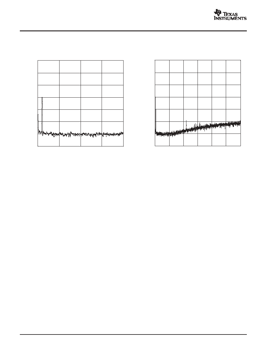
OUTPUT SPECTRUM (≠60 dB, N = 8192)
All specifications at TA = 25
∞
C, VCC1 = VCC2 = 2.4 V, fS = 44.1 kHz, system clock = 256 fS and 24-bit data, RL = 10 k
, unless otherwise noted.

PCM1772
PCM1773
SLES010D ≠ SEPTEMBER 2001 ≠ REVISED MAY 2004
www.ti.com
13
DETAILED DESCRIPTION
SYSTEM CLOCK, RESET, AND FUNCTIONS
System Clock Input
The PCM1772 and PCM1773 devices require a system clock for operating the digital interpolation filters and multilevel
-
modulators. The system clock is applied at terminal 16 (SCKI). Table 1 shows examples of system clock frequencies for
common audio sampling rates.
Figure 18 shows the timing requirements for the system clock input. For optimal performance, it is important to use a clock
source with low-phase jitter and noise.
Table 1. System Clock Frequency for Common Audio Sampling Frequencies
SAMPLING FREQUENCY, LRCK
SYSTEM CLOCK FREQUENCY, SCKI (MHz)
128 fS
192 fS
256 fS
384 fS
48 kHz
6.144
9.216
12.288
18.432
44.1 kHz
5.6448
8.4672
11.2896
16.9344
32 kHz
4.096
6.144
8.192
12.288
24 kHz
3.072
4.608
6.144
9.216
22.05 kHz
2.8224
4.2336
5.6448
8.4672
16 kHz
2.048
3.072
4.096
6.144
12 kHz
1.536
2.304
3.072
4.608
11.025 kHz
1.4112
2.1168
2.8224
4.2336
8 kHz
1.024
1.536
2.048
3.072
t(SCKH)
System Clock
Pulse Cycle Time
SCKI
t(SCKL)
0.7 VCC1
0.3 VCC1
1/(128 fS), 1/(192 fS), 1/(256 fS), and 1/(384 fS).
PARAMETERS
SYMBOL
MIN
UNIT
System clock pulse width high
t(SCKH)
7
ns
System clock pulse width low
t(SCKL)
7
ns
Figure 18. System Clock Timing
PCM1772
PCM1773
SLES010D ≠ SEPTEMBER 2001 ≠ REVISED MAY 2004
www.ti.com
14
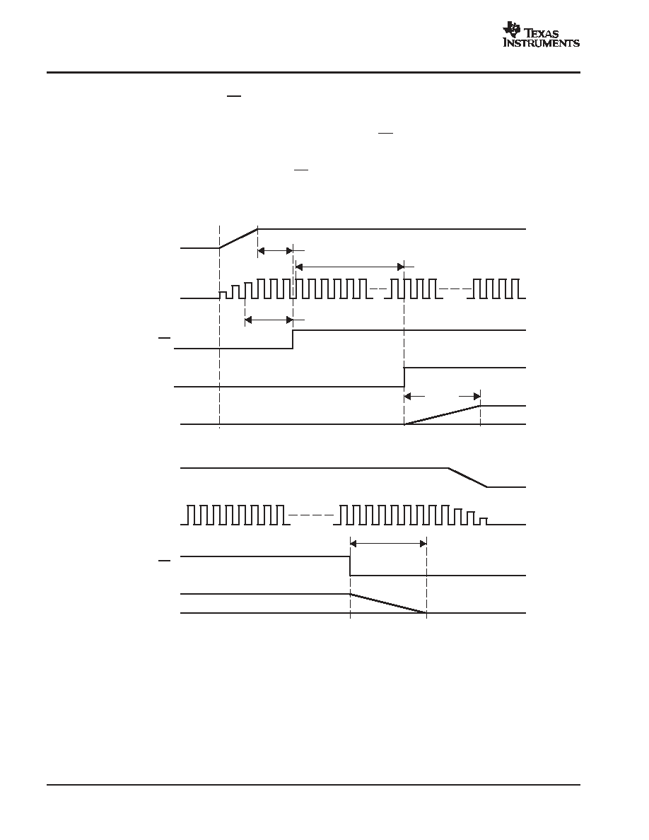
POWER ON/OFF AND RESET
The PCM1772/73 always must have the PD pin set from LOW to HIGH once after power-supply voltages V
CC1
and V
CC2
have reached the specified voltage range and stable clocks SCKI, BCK, and LRCK are being supplied for the power-on
sequence. A minimum time of 1 ms after both the clock and power-supply requirements are met is required before the PD
pin changes from LOW to HIGH, as shown in Figure 19. Subsequent to the PD LOW-to-HIGH transition, the internal logic
state is held in reset for 1024 system clock cycles prior to the start of the power-on sequence. During the power-on
sequence, V
OUT
L and V
OUT
R increase gradually from ground level, reaching an output level that corresponds to the input
data after a period of 9334/f
S
. When powering off, the PD pin is set from HIGH to LOW first. Then V
OUT
L and V
OUT
R
decrease gradually to ground level over a period of 9334/f
S
, as shown in Figure 20, after which power can be removed
without creating pop noise. When powering on or off, adhering to the timing requirements of Figure 19 and Figure 20
ensures that pop noise does not occur. If the timing requirements are not met, pop noise might occur.
VCC1, VCC2
0 V
LRCK, BCK, SCKI
PD
Internal Reset
VOUTL, VOUTR
1024 Internal System Clocks
9334/fS
0 V
1 ms (Min)
1 ms (Min)
Figure 19. Power-On Sequence
VCC1, VCC2
0 V
LRCK, BCK, SCKI
PD
VOUTL, VOUTR
0 V
9334/fS
Figure 20. Power-Off Sequence

PCM1772
PCM1773
SLES010D ≠ SEPTEMBER 2001 ≠ REVISED MAY 2004
www.ti.com
15
POWER-UP/-DOWN SEQUENCE AND RESET
The PCM1772 device has two kinds of power-up/-down methods: the PD terminal through hardware control and PWRD
(register 4, B0) through software control. The PCM1773 device has only the PD terminal through hardware control for the
power-up/-down sequence. The power-up or power-down sequence operates the same as the power-on or power-off
sequence. When powering up or down using the PD terminal, all digital circuits are reset. When powering up or down using
PWRD, all digital circuits are reset except for maintaining the logic states of the registers. Figure 21 shows the
power-up/power-down sequence.
VCC1, VCC2
2.4 V
LRCK, BCK, SCKI
PD
VOUTL, VOUTR
9334/fS
9334/fS
0 V
Figure 21. Power-Down and Power-Up Sequences

PCM1772
PCM1773
SLES010D ≠ SEPTEMBER 2001 ≠ REVISED MAY 2004
www.ti.com
16
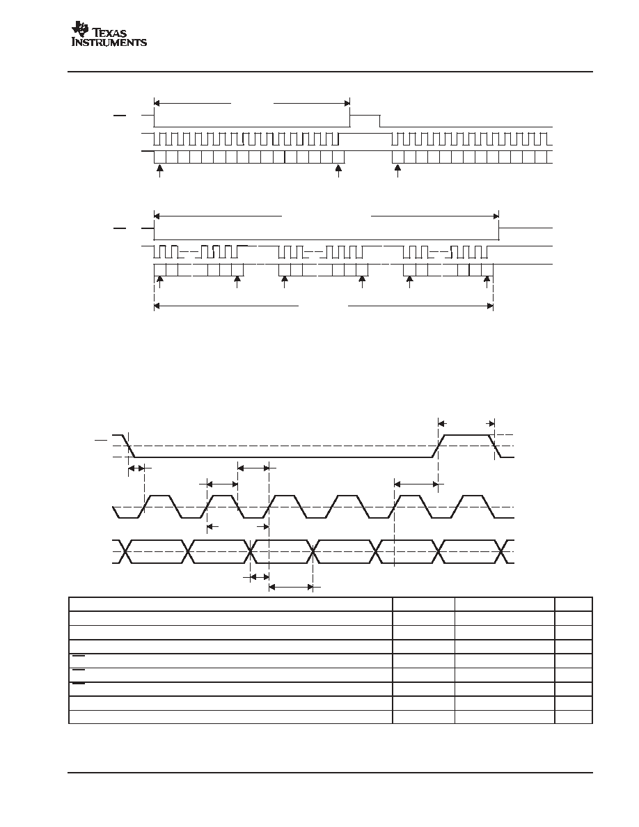
AUDIO SERIAL INTERFACE
The audio serial interface for the PCM1772 and PCM1773 devices is comprised of a 3-wire synchronous serial port. It
includes terminals 1 (LRCK), 2 (DATA), and 3 (BCK). BCK is the serial audio bit clock, and it clocks the serial data present
on DATA into the audio interface serial shift register. Serial data is clocked into the PCM1772 and PCM1773 devices on
the rising edge of BCK. LRCK is the serial audio left/right word clock. It latches serial data into the serial audio interface
internal registers.
Both LRCK and BCK of the PCM1772 device support the slave and master modes which are set by FMT (register 3). LRCK
and BCK are outputs during the master mode and inputs during the slave mode.
In slave mode, BCK and LRCK are synchronous to the audio system clock, SCKI. Ideally, it is recommended that LRCK
and BCK be derived from SCKI. LRCK is operated at the sampling frequency, f
S
. BCK can be operated at 32, 48, and 64
times the sampling frequency.
In master mode, BCK and LRCK are derived from the system clock, and these terminals are outputs. The BCK and LRCK
are synchronous to SCKI. LRCK is operated at the sampling frequency, f
S
. BCK can be operated at 64 times the sampling
frequency.
The PCM1772 and PCM1773 devices operate under LRCK synchronized with the system clock. The PCM1772 and
PCM1773 devices do not need a specific phase relationship between LRCK and the system clock, but do require the
synchronization of LRCK and the system clock. If the relationship between the system clock and LRCK changes more than
±
3BCK during one sample period, internal operation of the PCM1772 and PCM1773 devices halt within 1/f
S
, and the analog
output is kept in last data until resynchronization between system clock and LRCK is completed.
AUDIO DATA FORMATS AND TIMING
The PCM1772 device supports industry-standard audio data formats, including standard, I
2
S, and left justified. The
PCM1773 device supports the I
2
S and left-justified data formats. Table 2 lists the main features of the audio data interface.
Figure 22 shows the data formats. Data formats are selected using the format bits, FMT[2:0] of control register 3 in case
of the PCM1772 device, and are selected using the FMT terminal in case of the PCM1773 device. The default data format
is 24-bit, left-justified, slave mode. All formats require binary 2s complement, MSB-first audio data. Figure 23 shows a
detailed timing diagram for the serial audio interface in slave mode. Figure 24 shows a detailed timing diagram for the serial
audio interface in master mode.
Table 2. Audio Data Interface
AUDIO-DATA INTERFACE FEATURE
CHARACTERISTIC
Audio data interface format
(PCM1772)
Standard, I2S, left justified
Audio data interface format
(PCM1773)
I2S, left justified
Audio data bit length
16-, 20-, 24-bits selectable
Audio data format
MSB first, 2s complement

PCM1772
PCM1773
SLES010D ≠ SEPTEMBER 2001 ≠ REVISED MAY 2004
www.ti.com
17
(2) I
2
S Data Format; L-Channel = LOW, R-Channel = HIGH (Slave Mode)
LRCK
BCK
R-Channel
L-Channel
DATA
14 15 16
1
2
15 16
MSB
LSB
3
14
1
2
15 16
MSB
LSB
3
14
DATA
14 15 16
1
2
15 16
MSB
LSB
3
14
15 16
LSB
14
LRCK
BCK
R-Channel
L-Channel
DATA
1
2
N-1
N
MSB
LSB
3
N-2
1
2
N-1
N
MSB
LSB
3
N-2
1
2
1/fS
(= 32 fS, 48 fS or 64 fS)
16-Bit Right-Justified, BCK = 32 fS
16-Bit Right-Justified, BCK = 48 fS or 64 fS
1/fS
(1) Standard Data Format; L-Channel = HIGH, R-Channel = LOW (Slave Mode)
(3) Left-Justified Data Format; L-Channel = HIGH, R-Channel = LOW (Slave Mode)
DATA
18 19 20
1
2
19 20
MSB
LSB
3
18
1
2
19 20
MSB
LSB
3
18
20-Bit Right-Justified
DATA
22 23 24
1
2
23 24
MSB
LSB
3
22
1
2
23 24
MSB
LSB
3
22
24-Bit Right-Justified
1
2
MSB
3
LRCK
BCK
R-Channel
L-Channel
DATA
1
2
N-1
N
MSB
LSB
3
N-2
1
2
N-1
N
MSB
LSB
3
N-2
1
2
1/fS
(= 32 fS, 48 fS or 64 fS)
(= 32 fS, 48 fS or 64 fS)
(4) Left-Justified Data Format; L-Channel = HIGH, R-Channel = LOW (Master Mode)
(The frequency of BCK is 64 f
S
and SCKI is 256 f
S
only)
LRCK
BCK
R-Channel
L-Channel
DATA
1
2
N-1
N
MSB
LSB
3
N-2
1
2
N-1
N
MSB
LSB
3
N-2
1
2
1/fS
(= 64 fS)
Figure 22. Audio Data Input Formats

PCM1772
PCM1773
SLES010D ≠ SEPTEMBER 2001 ≠ REVISED MAY 2004
www.ti.com
18
t(BCH)
DATA
t(BCL)
t(LB)
t(BCY)
t(BL)
t(DH)
t(DS)
50% of VCC1
50% of VCC1
50% of VCC1
LRCK (Input)
BCK (Input)
PARAMETERS
SYMBOL
MIN
MAX
UNIT
BCK pulse cycle time
t(BCY)
1/(64 fS)(1)
BCK high-level time
t(BCH)
35
ns
BCK low-level time
t(BCL)
35
ns
BCK rising edge to LRCK edge
t(BL)
10
ns
LRCK edge to BCK rising edge
t(LB)
10
ns
DATA setup time
t(DS)
10
ns
DATA hold time
t(DH)
10
ns
(1) fS
is the sampling frequency.
Figure 23. Audio Interface Timing (Slave Mode)

PCM1772
PCM1773
SLES010D ≠ SEPTEMBER 2001 ≠ REVISED MAY 2004
www.ti.com
19
t(DL)
t(BCY)
t(SCY)
t(DS)
50% of VCC1
LRCK (Output)
50% of VCC1
50% of VCC1
50% of VCC1
SCKI
BCK (Output)
DATA
t(DH)
t(BCH)
t(BCL)
t(DB)
t(DB)
PARAMETERS
SYMBOL
MIN
MAX
UNIT
SCKI pulse cycle time
t(SCY)
1/(256 fS)(1)
LRCK edge from SCKI rising edge
t(DL)
0
40
ns
BCK edge from SCKI rising edge
t(DB)
0
40
ns
BCK pulse cycle time
t(BCY)
1/(64 fS)(1)
BCK high-level time
t(BCH)
146
ns
BCK low-level time
t(BCL)
146
ns
DATA setup time
t(DS)
10
ns
DATA hold time
t(DH)
10
ns
(1) fS is up to 48 kHz. fS
is the sampling frequency.
Figure 24. Audio Interface Timing (Master Mode)

PCM1772
PCM1773
SLES010D ≠ SEPTEMBER 2001 ≠ REVISED MAY 2004
www.ti.com
20
HARDWARE CONTROL (PCM1773)
The digital functions of the PCM1773 device are capable of hardware control. Table 3 shows selectable formats, Table 4
shows de-emphasis control, and Table 5 shows analog mixing control.
Table 3. Data Format Select
FMT
DATA FORMAT
Low
16- to 24-bit, left-justified format
High
16- to 24-bit, I2S format
Table 4. De-Emphasis Control
DEMP
DE-EMPHASIS FUNCTION
Low
44.1-kHz de-emphasis OFF
High
44.1-kHz de-emphasis ON
Table 5. Analog Mixing Control
AMIX
ANALOG MIXING
Low
Analog mixing OFF
High
Analog mixing ON
SOFTWARE CONTROL (PCM1772)
The PCM1772 device has many programmable functions that can be controlled in the software control mode. The functions
are controlled by programming the internal registers using MS, MC, and MD.
The software control interface is a 3-wire serial port that operates asynchronously to the serial audio interface. The serial
control interface is used to program the on-chip mode registers. MD is the serial data input, used to program the mode
registers. MC is the serial bit clock, used to shift data into the control port. MS is the mode control port select signal.
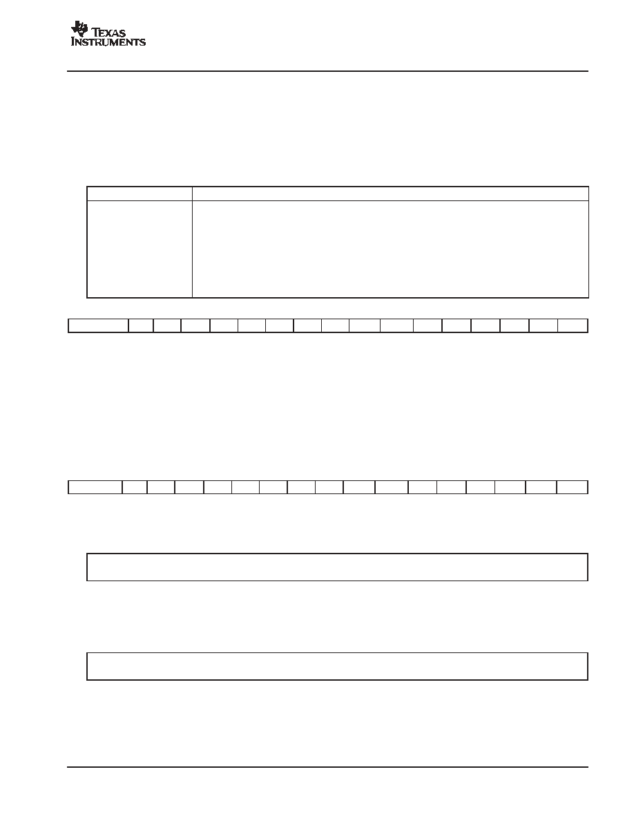
REGISTER WRITE OPERATION (PCM1772)
All write operations for the serial control port use 16-bit data words. Figure 25 shows the control data word format. The most
significant bit must be 0. Seven bits, labeled IDX[6:0], set the register index (or address) for the write operation. The eight
least significant bits, D[7:0], contain the data to be written to the register specified by IDX[6:0].
Figure 26 shows the functional timing diagram for writing to the serial control port. To write data into the mode register, data
is clocked into an internal shift register on the rising edge of the MC clock. Serial data can change on the falling edge of
the MC clock and must be stable on the rising edge of the MC clock. The MS signal must be low during the write mode,
and the rising edge of the MS signal must be aligned with the falling edge of the last MC clock pulse in the 16-bit frame.
The MC clock can run continuously between transactions while the MS signal is low.
MSB
0
IDX6
IDX5
IDX4
IDX3
IDX2
IDX1
IDX0
D7
D6
D5
D4
D3
D2
D1
D0
0
0
LSB
Register Index (or Address)
Register Data
Figure 25. Control Data Word Format for MD
PCM1772
PCM1773
SLES010D ≠ SEPTEMBER 2001 ≠ REVISED MAY 2004
www.ti.com
21
MC
MS
MD
16-Bits
(1) Single Write Operation
MSB
LSB
MSB
(2) Continuous Write Operation
MSB
LSB
MSB
LSB
MSB
LSB
16-Bits x N Frames
MC
MS
MD
N Frames
Figure 26. Register Write Operation
CONTROL INTERFACE TIMING REQUIREMENTS (PCM1772)
Figure 27 shows a detailed timing diagram for the serial control interface. These timing parameters are critical for proper
control port operation.
t(MCH)
50% of VCC1
MS
t(MLS)
LSB
50% of VCC1
50% of VCC1
t(MCL)
t(MHH)
t(MLH)
t(MCY)
t(MDH)
t(MDS)
MC
MD
PARAMETERS
SYMBOL
MIN
TYP
MAX
UNITS
MC pulse cycle time
t(MCY)
100(1)
ns
MC low-level time
t(MCL)
50
ns
MC high-level time
t(MCH)
50
ns
MS high-level time
t(MHH)
(2)
ns
MS falling edge to MC rising edge
t(MLS)
20
ns
MS hold time
t(MLH)
20
ns
MD hold time
t(MDH)
15
ns
MD setup time
t(MDS)
20
ns
(1) When MC runs continuously between transactions, MC pulse cycle time is specified as 3/(128 fS), where fS is sampling rate.
(2) 3/(128fS) s (min), where fS is sampling rate
Figure 27. Control Interface Timing

PCM1772
PCM1773
SLES010D ≠ SEPTEMBER 2001 ≠ REVISED MAY 2004
www.ti.com
22
MODE CONTROL REGISTERS (PCM1772)
User-Programmable Mode Controls
The PCM1772 device has a number of user-programmable functions that can be accessed via mode control registers. The
registers are programmed using the serial control interface, as discussed in the SOFTWARE CONTROL (PCM1772)
section. Table 6 lists the available mode control functions, along with their reset default conditions and associated register
index.
Register Map
Table 7 shows the mode control register map. Each register includes an index (or address) indicated by the IDX[6:0] bits.
Table 6. User-Programmable Mode Controls
FUNCTION
RESET DEFAULT
REGISTER NO.
BIT(S)
Soft mute control, L/R independently
Disabled
01
MUTL, MUTR
Digital attenuation level setting, 0 dB to ≠62 dB in 1-dB steps, L/R
independently
0 dB
01, 02
ATL[5:0], ATR[5:0]
Oversampling rate control (128 fS, 192 fS, 256 fS, 384 fS)
128 fS oversampling
03
OVER
Polarity control for analog output for R-channel DAC
Not inverted
03
RINV
Analog mixing control for analog in, AIN (terminal 14)
Disabled
03
AMIX
44.1-kHz de-emphasis control
Disabled
03
DEM
Audio data format select
24-bit, left-justified format
03
FMT[2:0]
Zero cross attenuation
Disabled
04
ZCAT
Power down control
Disabled
04
PWRD
Table 7. Mode Control Register Map
REGISTER
IDX [6:0]
(B14
≠
B8)
B15
B14
B13
B12
B11
B10
B9
B8
B7
B6
B5
B4
B3
B2
B1
B0
Register 01
01h
0
IDX6
IDX5
IDX4
IDX3
IDX2
IDX1
IDX0
MUTR
MUTL
ATL5
ATL4
ATL3
ATL2
ATL1
ATL0
Register 02
02h
0
IDX6
IDX5
IDX4
IDX3
IDX2
IDX1
IDX0
RSV
RSV
ATR5
ATR4
ATR3
ATR2
ATR1
ATR0
Register 03
03h
0
IDX6
IDX5
IDX4
IDX3
IDX2
IDX1
IDX0
OVER
RSV
RINV
AMIX
DEM
FMT2
FMT1
FMT0
Register 04
04h
0
IDX6
IDX5
IDX4
IDX3
IDX2
IDX1
IDX0
RSV
RSV
RSV
ZCAT
RSV
RSV
RSV
PWRD
NOTE: RSV: Reserved for test operation. It must be set to 0 during regular operation.
Register Definitions
B15
B14
B13
B12
B11
B10
B9
B8
B7
B6
B5
B4
B3
B2
B1
B0
Register 01
0
IDX6
IDX5
IDX4
IDX3
IDX2
IDX1
IDX0
MUTR
MUTL
ATL5
ATL4
ATL3
ATL2
ATL1
ATL0
IDX[6:0]: 000 0001b
MUTx: Soft Mute Control
Where, x = L or R, corresponding to the line output V
OUT
L and V
OUT
R.
Default Value: 0
MUTL, MUTR = 0
MUTL, MUTR = 1
Mute disabled (default)
Mute enabled
The mute bits, MUTL and MUTR, enable or disable the soft mute function for the corresponding line outputs,
V
OUT
L and V
OUT
R. The soft mute function is incorporated into the digital attenuators. When mute is disabled
(MUTx = 0), the attenuator and DAC operate normally. When mute is enabled by setting MUTx = 1, the digital
attenuator for the corresponding output is decreased from the current setting to the infinite attenuation, one
attenuator step (1 dB) at a time. This provides pop-free muting of the line output.
By setting MUTx = 0, the attenuator is increased one step at a time to the previously programmed attenuation
level.
PCM1772
PCM1773
SLES010D ≠ SEPTEMBER 2001 ≠ REVISED MAY 2004
www.ti.com
23
ATL[5:0]: Digital Attenuation Level Setting for Line Output, V
OUT
L
Default value: 11 1111b
Line output, V
OUT
L includes a digital attenuation function. The attenuation level can be set from 0 dB to ≠62 dB, in
1-dB steps. Changes in attenuator levels are made by incrementing or decrementing by one step (1 dB) for every
8/f
S
time internal until the programmed attenuator setting is reached. Alternatively, the attenuation level may be
set to infinite attenuation (or mute).
The following table shows attenuation levels for various settings:
ATL[5:0]
ATTENUATION LEVEL SETTING
11 1111b
0 dB, no attenuation (default)
11 1110b
≠1 dB
11 1101b
≠2 dB
L
L
00 0010b
≠61 dB
00 0001b
≠62 dB
00 0000b
Mute
B15
B14
B13
B12
B11
B10
B9
B8
B7
B6
B5
B4
B3
B2
B1
B0
Register 02
0
IDX6
IDX5
IDX4
IDX3
IDX2
IDX1
IDX0
RSV
RSV
ATR5
ATR4
ATR3
ATR2
ATR1
ATR0
IDX[6:0]: 000 0010b
ATR[5:0]: Digital Attenuation Level Setting for Line Output, V
OUT
R
Default Value: 11 1111b
Line output, V
OUT
R includes a digital attenuation function. The attenuation level can be set from 0 dB to ≠62 dB, in
1-dB steps. Changes in attenuator levels are made by incrementing or decrementing by one step (1 dB) for every
8/f
S
time internal until the programmed attenuator setting in reached. Alternatively, the attenuation level can be
set to infinite attenuation (or mute).
To set the attenuation levels for ATR[5:0], see the table for ATL[5:0], register 01.
B15
B14
B13
B12
B11
B10
B9
B8
B7
B6
B5
B4
B3
B2
B1
B0
Register 03
0
IDX6
IDX5
IDX4
IDX3
IDX2
IDX1
IDX0
OVER
RSV
RINV
AMIX
DEM
FMT2
FMT1
FMT0
IDX[6:0]: 000 0011b
OVER: Oversampling Control
Default Value: 0
OVER = 0
OVER = 1
128f
S
oversampling
192f
S
, 256f
S
, 384f
S
oversampling
The OVER bit controls the oversampling rate of the
-
D/A converters. When it operates at a low sampling rate,
less than 24 kHz, this function is recommended.
RINV: Polarity Control for Line Output, V
OUT
R
Default Value: 0
RINV = 0
RINV = 1
Not inverted
Inverted output
The RINV bits allow the user to control the polarity of the line output, V
OUT
R. This function can be used to connect
the monaural speaker with BTL connection method. This bit is recommended to be 0 during the power-up/-down
sequence for minimizing audible pop noise.

PCM1772
PCM1773
SLES010D ≠ SEPTEMBER 2001 ≠ REVISED MAY 2004
www.ti.com
24
AMIX: Analog Mixing Control for External Analog Signal, AIN
Default Value: 0
AMIX = 0
AMIX = 1
Disabled (not mixed)
Enabled (mixing to the DAC output)
AMIX bit allows the user to mix analog input (AIN) with line outputs (V
OUT
L/V
OUT
R) internally.
DEM: 44.1-kHz De-Emphasis Control
Default Value: 0
DEM = 0
DEM = 1
Disabled
Enabled
The DEM bit enables or disables the digital de-emphasis filter for 44.1-kHz sampling rate.
FMT[2:0]: Audio Interface Data Format
Default Value: 000
The FMT[2:0] bits select the data format for the serial audio interface. The following table shows the available
format options.
FMT[2:0]
Audio Data Format Selection
000
001
010
011
100
101
110
111
16- to 24-bit, left-justified format (default)
16- to 24-bit, I
2
S format
24-bit right-justified data
20-bit right-justified data
16-bit right-justified data
16- to 24-bit, left-justified format, master mode
Reserved
Reserved
B15
B14
B13
B12
B11
B10
B9
B8
B7
B6
B5
B4
B3
B2
B1
B0
Register 04
0
IDX6
IDX5
IDX4
IDX3
IDX2
IDX1
IDX0
RSV
RSV
RSV
ZCAT
RSV
RSV
RSV
PWRD
IDX[6:0]: 000 0100b
ZCAT: Zero Cross Attenuation
Default Value: 0
ZCAT = 0
ZCAT = 1
Normal attenuation (default)
Zero cross attenuation
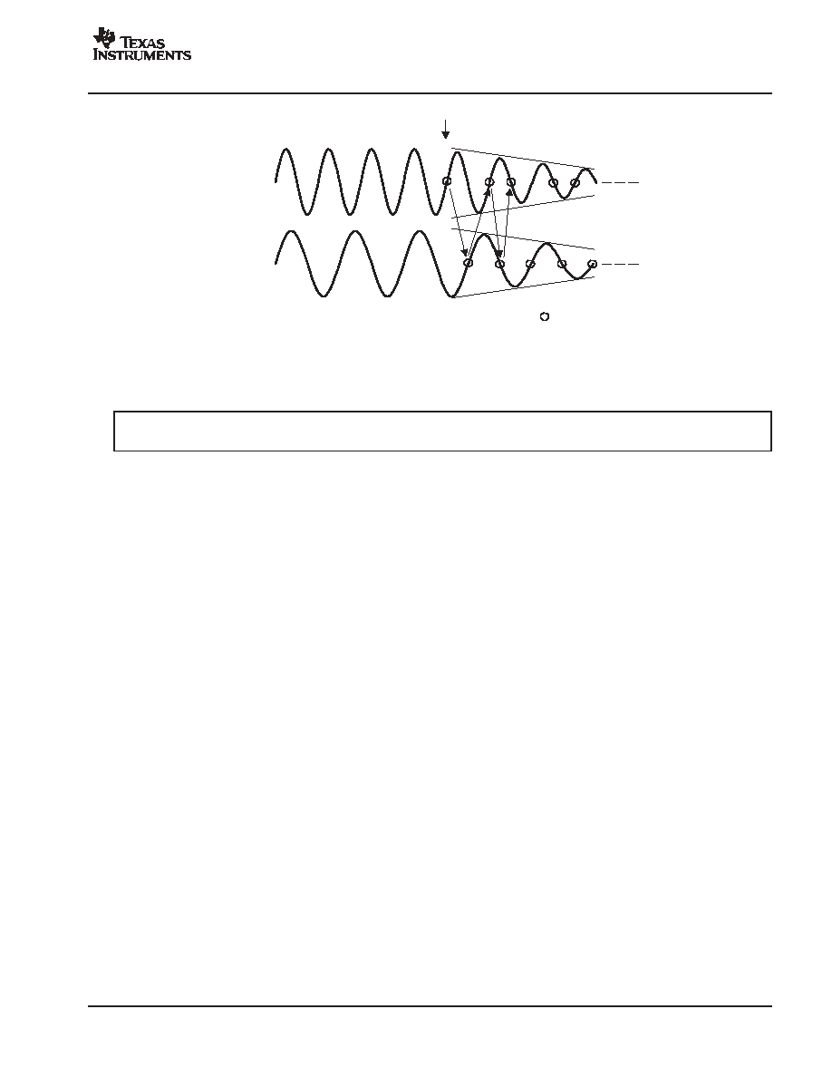
This bit enables to change signal level on zero crossing during attenuation control or muting. If the signal does not
cross BPZ beyond 512/f
S
(11.6 ms at 44.1-kHz sampling rate), the signal level is changed similar to normal
attenuation control. This function is independently monitored for each channel; moreover, change of signal level
is alternated between both channels. Figure 28 shows an example of zero cross attenuation.
PCM1772
PCM1773
SLES010D ≠ SEPTEMBER 2001 ≠ REVISED MAY 2004
www.ti.com
25
ATT CTRL START
Level Change Point
L-Channel
(1.5 kHz)
R-Channel
(1 kHz)
Figure 28. Example of Zero Cross Attenuation
PWRD: Power Down Control
Default Value: 0
PWRD = 0
PWRD = 1
Normal operation (default)
Power-down state
This bit is used to enter into low-power mode. Note that PWRD has no reset function.
When this bit is set to 1, the PCM1772 device enters low-power mode, and all digital circuits are reset except the
register states which remain unchanged.
ANALOG IN/OUT
LINE OUTPUT (STEREO)
The PCM1772 and PCM1773 devices have two independent lineout amplifiers, and each amplifier output is provided at
the V
OUT
L and V
OUT
R terminals. The capability of line output is designed for driving a 10-k
minimum load.
Monaural Output (BTL Mode/Monaural Speaker)
When the user needs monaural output, the PCM1772 device can provide it. The PCM1772 device has RINV bit on control
register 03. Because this bit allows the user to invert the polarity of the line output for the right channel, the user can create
a monaural output by summing the line output for left and right channels through the external power amplifier or headphone
amplifier. The RINV bit is recommended to be 0 during power-up/-down sequence for minimizing audible pop noise.
Analog Input
The PCM1772 and PCM1773 devices have an analog input, AIN (terminal 10). The AMIX bit (PCM1772) or the AMIX
terminal (PCM1773) allows the user to mix AIN with the line outputs (V
OUT
L and V
OUT
R) internally. When in MIXING mode,
an ac-coupling capacitor is needed for AIN. But if AIN is not used, AIN must be open and the AMIX bit (PCM1772) must
be disabled or the AMIX terminal (PCM1773) must be low.
Because AIN does not have an internal low-pass filter, it is recommended that the bandwidth of input signal into AIN is
limited to less than 100 kHz. The source of signals connected to AIN must be connected by low impedance.
Although the maximum input voltage on AIN is designed to be as large as 0.584V
CC2
[peak-to-peak], the user must
attenuate the input voltage on AIN and control digital input data so that each line output (V
OUT
L and V
OUT
R) does not
exceed 0.75 V
CC2
[peak-to-peak] during mixing mode.
V
COM
Output
One unbuffered common-mode voltage output terminal, V
COM,
is brought out for decoupling purposes. This terminal is
nominally biased to a dc voltage level equal to 0.5 V
CC2
and connected to a 10-
µ
F capacitor. In the case of a capacitor
smaller than 10
µ
F, pop noise can be generated during the power-on/-off or power-up/-down sequences.

PCM1772
PCM1773
SLES010D ≠ SEPTEMBER 2001 ≠ REVISED MAY 2004
www.ti.com
26
APPLICATION INFORMATION
CONNECTION DIAGRAMS
Figure 29 shows the basic connection diagram with the necessary power supply bypassing and decoupling components.
It is recommended that the component values shown in Figure 29 be used for all designs.
The use of series resistors (22
to 100
) is recommended for the MCKI, LRCK, BCK, and DATA inputs. The series resistor
combines with the stray PCB and device input capacitance to form a low-pass filter that reduces high-frequency noise
emissions and helps to dampen glitches and ringing present on the clock and data lines.
POWER SUPPLIES AND GROUNDING
The PCM1772 and PCM1773 devices require a 2.4-V typical analog supply for V
CC1
and V
CC2
. These 2.4-V supplies
power the DAC, analog output filter, and other circuits. For best performance, these 2.4-V supplies must be derived from
the analog supply using a linear regulator, as shown in Figure 29.
Figure 29 shows the proper power supply bypassing. The 10-
µ
F capacitors must be tantalum or aluminum electrolytic,
while the 0.1-
µ
F capacitors are ceramic (X7R type is recommended for surface-mount applications).
LRCK
16
15
14
13
12
11
10
9
1
2
3
4
5
6
7
8
PCM1772
DATA
BCK
PD
AGND1
AGND2
VCOM
VOUTR
SCKI
VOUTL
MS
MC
MD
VCC1
AIN
VCC2
Controller
10
µ
F
1.6 V to 3.6 V
Analog In
Post
LPF
Audio DSP
10
µ
F
10
µ
F
10
µ
F
Power Amplifier
or Headphone
Amplifier
10
µ
F
Post
LPF
Power Amplifier
or Headphone
Amplifier
10
µ
F
Figure 29. Basic Connection Diagram

MECHANICAL DATA
MPQF110 - SEPTEMBER 2001
POST OFFICE BOX 655303
∑
DALLAS, TEXAS 75265
RGA (S-PQFP-N20)
PLASTIC QUAD FLATPACK
0,50 NOM
DETAIL "A"
4202802/B 08/01
1,00
MAX
4,30
4,10
M
0,05
0,05
A
S
S
"C"
"B"
1
20
1,00 NOM
1,00 NOM
0,50 NOM
Index
C0,70
4,05
3,95
4,30
4,10
4,05
3,95
DETAIL "B"
DETAIL "C"
S AB
0,27
0,17
0,25
0,09
0,75
0,45
0,05
0,00
0,95
0,50
S
0,21
0,09
0,25
0,09
0,05
0,00
0,23
0,17
0,27
0,17
0,69
±
0,11
0,35
±
0,11
0,22
±
0,05
"A"
B
0,50 NOM/2
NOTES: A. All linear dimensions are in millimeters.
B. This drawing is subject to change without notice.
C. These dimensions include package bend.
D. Falls within EIAJ: EDR-7324.

MECHANICAL DATA
MTSS001C ≠ JANUARY 1995 ≠ REVISED FEBRUARY 1999
POST OFFICE BOX 655303
∑
DALLAS, TEXAS 75265
PW (R-PDSO-G**)
PLASTIC SMALL-OUTLINE PACKAGE
14 PINS SHOWN
0,65
M
0,10
0,10
0,25
0,50
0,75
0,15 NOM
Gage Plane
28
9,80
9,60
24
7,90
7,70
20
16
6,60
6,40
4040064/F 01/97
0,30
6,60
6,20
8
0,19
4,30
4,50
7
0,15
14
A
1
1,20 MAX
14
5,10
4,90
8
3,10
2,90
A MAX
A MIN
DIM
PINS **
0,05
4,90
5,10
Seating Plane
0
∞
≠ 8
∞
NOTES: A. All linear dimensions are in millimeters.
B. This drawing is subject to change without notice.
C. Body dimensions do not include mold flash or protrusion not to exceed 0,15.
D. Falls within JEDEC MO-153

IMPORTANT NOTICE
Texas Instruments Incorporated and its subsidiaries (TI) reserve the right to make corrections, modifications,
enhancements, improvements, and other changes to its products and services at any time and to discontinue
any product or service without notice. Customers should obtain the latest relevant information before placing
orders and should verify that such information is current and complete. All products are sold subject to TI's terms
and conditions of sale supplied at the time of order acknowledgment.
TI warrants performance of its hardware products to the specifications applicable at the time of sale in
accordance with TI's standard warranty. Testing and other quality control techniques are used to the extent TI
deems necessary to support this warranty. Except where mandated by government requirements, testing of all
parameters of each product is not necessarily performed.
TI assumes no liability for applications assistance or customer product design. Customers are responsible for
their products and applications using TI components. To minimize the risks associated with customer products
and applications, customers should provide adequate design and operating safeguards.
TI does not warrant or represent that any license, either express or implied, is granted under any TI patent right,
copyright, mask work right, or other TI intellectual property right relating to any combination, machine, or process
in which TI products or services are used. Information published by TI regarding third-party products or services
does not constitute a license from TI to use such products or services or a warranty or endorsement thereof.
Use of such information may require a license from a third party under the patents or other intellectual property
of the third party, or a license from TI under the patents or other intellectual property of TI.
Reproduction of information in TI data books or data sheets is permissible only if reproduction is without
alteration and is accompanied by all associated warranties, conditions, limitations, and notices. Reproduction
of this information with alteration is an unfair and deceptive business practice. TI is not responsible or liable for
such altered documentation.
Resale of TI products or services with statements different from or beyond the parameters stated by TI for that
product or service voids all express and any implied warranties for the associated TI product or service and
is an unfair and deceptive business practice. TI is not responsible or liable for any such statements.
Following are URLs where you can obtain information on other Texas Instruments products and application
solutions:
Products
Applications
Amplifiers
amplifier.ti.com
Audio
www.ti.com/audio
Data Converters
dataconverter.ti.com
Automotive
www.ti.com/automotive
DSP
dsp.ti.com
Broadband
www.ti.com/broadband
Interface
interface.ti.com
Digital Control
www.ti.com/digitalcontrol
Logic
logic.ti.com
Military
www.ti.com/military
Power Mgmt
power.ti.com
Optical Networking
www.ti.com/opticalnetwork
Microcontrollers
microcontroller.ti.com
Security
www.ti.com/security
Telephony
www.ti.com/telephony
Video & Imaging
www.ti.com/video
Wireless
www.ti.com/wireless
Mailing Address:
Texas Instruments
Post Office Box 655303 Dallas, Texas 75265
Copyright
2004, Texas Instruments Incorporated