Äîêóìåíòàöèÿ è îïèñàíèÿ www.docs.chipfind.ru
SBAS290B - JULY 2003 - SEPTEMBER 2004
High-Performance 24-Bit, 216kHz Sampling
Stereo Audio Analog-to-Digital Converter
PCM4202
FEATURES
D
Two High-Performance Delta-Sigma
Analog-to-Digital Converters
- 24-Bit Linear PCM or 1-Bit Direct Stream
Digital (DSD) Output Data
- Supports PCM Output Sampling Rates up
to 216kHz
- Supports 64f
S
and 128f
S
DSD Output Data
Rates
D
Dynamic Performance: PCM Output
- Dynamic Range (V
IN
= -60dBFS,
f
IN
= 1kHz, A-Weighted): 118dB
- THD+N (V
IN
= -0.5dB, f
IN
= 1kHz): -105dB
D
Dynamic Performance: DSD Output, 64f
S
- Dynamic Range (A-Weighted): 115dB
- THD+N (V
IN
= -0.5dB, f
IN
= 1kHz): -102dB
D
Audio Serial Port
- 24-Bit Linear PCM Output Data
- Master or Slave Mode Operation
- Supports Left-Justified, Right-Justified,
and I
2
S
E
Data Formats
D
Additional PCM Output Features:
- Linear-Phase Digital Decimation Filter
- Digital High-Pass Filter for DC Removal
- Clipping Flag Output for Each Channel
D
Power Supplies: +5V Analog and +3.3V Digital
D
Power Dissipation:
- f
S
= 48kHz: 308mW typical
- f
S
= 96kHz: 338mW typical
- f
S
= 192kHz: 318mW typical
D
Power-Down Mode
D
Available in a SSOP-28 Package
D
Pin- and Function-Compatible with the
PCM1804
APPLICATIONS
D
Digital Recorders and Mixing Desks
D
Digital Audio Effects Processors
D
Broadcast Studio Equipment
D
Surround-Sound Encoders
D
High-End A/V Receivers
DESCRIPTION
The PCM4202 is a high-performance, stereo audio
analog-to-digital (A/D) converter designed for professional
and broadcast audio applications. The PCM4202
architecture utilizes a 1-bit delta-sigma modulator per
channel, incorporating a novel density modulated dither
scheme for improved dynamic performance.
The PCM4202 supports 24-bit linear PCM output data,
with sampling frequencies up to 216kHz. The PCM4202
can also be configured to output either 64x or 128x
oversampled, 1-bit direct stream digital (DSD) data for
each channel. Support for PCM and DSD output formats
makes the PCM4202 suitable for a variety of digital audio
recording and processing applications.
The PCM4202 includes a flexible audio serial port inter-
face, which supports standard audio data formats. Audio
data format selection, sampling mode configuration, and
high-pass filter functions are all programmed using dedi-
cated control pins.
The PCM4202 operates from a +5V analog power supply
and a +3.3V digital power supply. The digital I/O pins are
compatible with +3.3V logic families. The PCM4202 is
available in a small SSOP-28 package.
I2S is a registered trademark of Royal Philips Electronics B.V., The Netherlands. All other trademarks are the property of their respective owners.
PRODUCTION DATA information is current as of publication date. Products
conform to specifications per the terms of Texas Instruments standard warranty.
Production processing does not necessarily include testing of all parameters.
www.ti.com
Copyright
2003-2004, Texas Instruments Incorporated
Please be aware that an important notice concerning availability, standard warranty, and use in critical applications of Texas Instruments
semiconductor products and disclaimers thereto appears at the end of this data sheet.
PCM4202
SBAS290B - JULY 2003 - SEPTEMBER 2004
www.ti.com
2
This integrated circuit can be damaged by ESD. Texas Instruments recommends that all integrated circuits be handled with appropriate
precautions. Failure to observe proper handling and installation procedures can cause damage.
ESD damage can range from subtle performance degradation to complete device failure. Precision integrated circuits may be more susceptible to
damage because very small parametric changes could cause the device not to meet its published specifications.
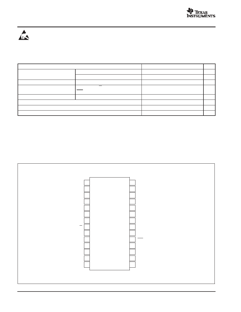
ABSOLUTE MAXIMUM RATINGS
over operating free-air temperature range unless otherwise noted(1)
PCM4202
UNIT
Supply voltage
VCC
+6.0
V
Supply voltage
VDD
+3.6
V
Ground voltage differences
(any AGND to DGND)
±
0.1
V
Digital input voltage
FMT0, FMT1, S/M, FS0, FS1, FS2, SCKI,
RST, HPFD, BCK, LRCK
-0.3 to (VDD + 0.3)
V
Analog input voltage
VINL+, VINL-, VINR+, VINR-
-0.3 to (VCC + 0.3)
V
Input current (any pin except supplies)
±
10mA
V
Operating temperature range
-10 to +70
°
C
Storage temperature range, TSTG
-65 to +150
°
C
(1) Stresses above those listed under Absolute Maximum Ratings may cause permanent damage to the device. Exposure to absolute maximum
conditions for extended periods may degrade device reliability. These are stress ratings only, and functional operation of the device at these or
any other conditions beyond those specified is not implied.
PACKAGE/ORDERING INFORMATION
For the most current package and ordering information, see the Package Option Addendum located at the end of this
datasheet.
PIN ASSIGNMENT
V
REF
L
AGNDL
V
COM
L
V
IN
L+
V
IN
L
-
FMT0
FMT1
S/M
FS0
FS1
FS2
HPFD
DGND
V
DD
V
REF
R
AGNDR
V
COM
R
V
IN
R+
V
IN
R
-
AGND
V
CC
CLIPL
CLIPR
RST
SCKI
LRCK or DSDBCK
BCK or DSDL
DATA or DSDR
1
2
3
4
5
6
7
8
9
10
11
12
13
14
28
27
26
25
24
23
22
21
20
19
18
17
16
15
PCM4202
PCM4202
SBAS290B - JULY 2003 - SEPTEMBER 2004
www.ti.com
3
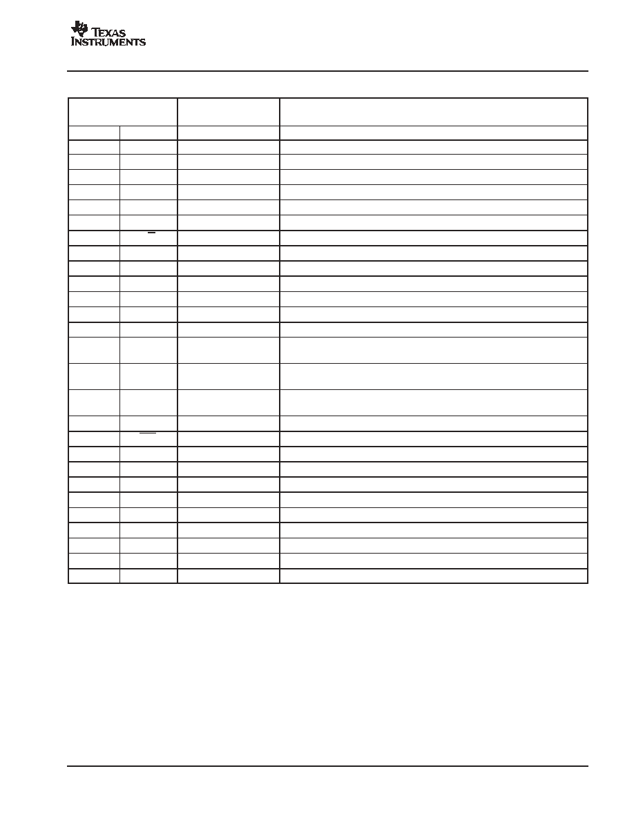
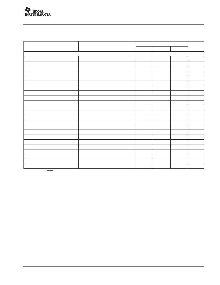
Terminal Functions
TERMINAL
PIN NO.
NAME
I/O
DESCRIPTION
1
VREFL
Output
Left Channel Voltage Reference
2
AGNDL
Ground
Left Channel Reference Ground
3
VCOML
Output
Left Channel DC Common-mode Voltage, +2.5V Typical
4
VINL+
Input
Left Channel Non-inverting Analog Input
5
VINL-
Input
Left Channel Inverting Analog Input
6
FMT0
Input
Audio Data Format Selection
7
FMT1
Input
Audio Data Format Selection
8
S/M
Input
Audio Serial Port Slave/Master Mode Selection (0 = Master, 1 = Slave)
9
FS0
Input
Sampling Mode Selection
10
FS1
Input
Sampling Mode Selection
11
FS2
Input
Sampling Mode Selection
12
HPFD
Input
High-pass Filter Disable (Active High)
13
DGND
Ground
Digital Ground
14
VDD
Power
Digital Power Supply, +3.3V
15
DATA
or DSDR
Output
Audio Serial Port Left and Right Channel PCM Data
or Right Channel DSD Data
16
BCK
or DSDL
I/O
Audio Serial Port Bit (or Data) Clock
or Left Channel DSD Data Output
17
LRCK
or DSDBCK
I/O
Audio Serial Port Left/Right (or Word) Clock
or DSD Data Clock Output
18
SCKI
Input
System Clock
19
RST
Input
Reset/Power-down (Active Low with internal pull-up)
20
CLIPR
Output
Right Channel Clipping Flag (Active High)
21
CLIPL
Output
Left Channel Clipping Flag (Active High)
22
VCC
Power
Analog Power Supply, +5V
23
AGND
Ground
Analog Ground
24
VINR-
Input
Right Channel Inverting Analog Input
25
VINR+
Input
Right Channel Non-inverting Analog Input
26
VCOMR
Output
Right Channel DC Common-mode Voltage, +2.5V Typical
27
AGNDR
Ground
Right Channel Reference Ground
28
VREFR
Output
Right Channel Voltage Reference
PCM4202
SBAS290B - JULY 2003 - SEPTEMBER 2004
www.ti.com
4
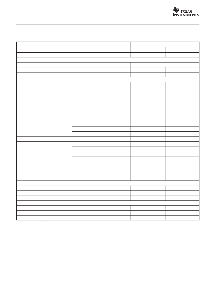
ELECTRICAL CHARACTERISTICS
All parameters are specified at TA = +25
°
C with VCC = +5V, VDD = +3.3V, and a measurement bandwidth from 20Hz to 20kHz, unless otherwise
noted. System clock frequency is equal to 256fS for Single and Dual Rate sampling modes, and 128fS for Quad Rate sampling mode.
PCM4202
PARAMETER
CONDITIONS
MIN
TYP
MAX
UNITS
RESOLUTION
24
Bits
AUDIO DATA FORMAT
Linear PCM interface formats
Two's complement, MSB first data
I2S, Left or Right Justified
Linear PCM word length
24
Bits
Direct Stream Digital (DSD) output
1
Bit
DIGITAL CHARACTERISTICS
Input logic level
VIH
0.7 x VDD
VDD
V
VIL
0
0.3 x VDD
V
Output logic level
VOH
IOH = -2mA
0.8 x VDD
V
VOL
IOL = +2mA
0.2 x VDD
V
Input current
IIH
VIN = VDD
+10
µ
A
IIL
VIN = 0V
-10
µ
A
Input current(1)
IIH
VIN = VDD
+25
µ
A
IIL
VIN = 0V
-25
µ
A
Single rate
8
54
kHz
Sampling frequency(2)
fS
Dual rate
54
108
kHz
Sampling frequency
fS
Quad rate
108
216
kHz
System clock duty cycle
45
50
55
%
Single rate, SCKI = 256fS
2.048
13.824
MHz
Single rate, SCKI = 384fS
3.072
20.736
MHz
Single rate, SCKI = 512fS
4.096
27.648
MHz
System clock frequency(2)
Single rate, SCKI = 768fS
6.144
38.4
MHz
System clock frequency(2)
Dual rate, SCKI = 256fS
13.824
27.648
MHz
Dual rate, SCKI = 384fS
20.736
38.4
MHz
Quad rate, SCKI = 128fS
13.824
27.648
MHz
Quad rate, SCKI = 192fS
20.736
38.4
MHz
ANALOG OUTPUTS
Input voltage, full-scale
Differential input
6.0
VPP
Input impedance
3
k
Common-mode rejection
85
dB
DC PERFORMANCE
Output offset error
HPFD = 1
±
4
% of FSR
Gain error
±
4
% of FSR
Gain mismatch channel-to-channel
±
3
% of FSR
(1) Applies to the RST input, pin 19.
(2) Single, Dual, and Quad Rate sampling modes are described within this data sheet.
(3) Dynamic performance parameters are measured using an Audio Precision System Two Cascade or Cascade Plus test system. The
measurement bandwidth is limited by using the Audio Precision 22Hz high-pass filter in combination with the Audio Precision 20kHz, fS/2, or
a user-defined 40kHz low-pass filter. All A-weighted measurements are performed using the Audio Precision A-weighting filter in combination
with the previously mentioned filters.
PCM4202
SBAS290B - JULY 2003 - SEPTEMBER 2004
www.ti.com
5
ELECTRICAL CHARACTERISTICS (continued)
All parameters are specified at TA = +25
°
C with VCC = +5V, VDD = +3.3V, and a measurement bandwidth from 20Hz to 20kHz, unless otherwise
noted. System clock frequency is equal to 256fS for Single and Dual Rate sampling modes, and 128fS for Quad Rate sampling mode.
PCM4202
PARAMETER
UNITS
MAX
TYP
MIN
CONDITIONS
DYNAMIC PERFORMANCE(3)
fS = 48kHz, Single Rate
BW = 20Hz to 20kHz
Total harmonic distortion + noise
THD+N
VIN = -0.5dBFS, fIN = 1kHz
-105
-95
dB
Dynamic range
VIN = -60dBFS, fIN = 1kHz, A-Weighted
112
118
dB
Dynamic range, no weighting
VIN = -60dBFS, fIN = 1kHz
116
dB
Channel separation
100
120
dB
fS = 96kHz, Dual Rate
BW = 20Hz to 40kHz
Total harmonic distortion + noise
THD+N
VIN = -0.5dBFS, fIN = 1kHz
-105
dB
Dynamic range
VIN = -60dBFS, fIN = 1kHz, A-Weighted
118
dB
Dynamic range, no weighting
VIN = -60dBFS, fIN = 1kHz
112
dB
Channel separation
120
dB
fS = 192kHz, Quad Rate
BW = 20Hz to 40kHz
Total harmonic distortion + noise
THD+N
VIN = -0.5dBFS, fIN = 1kHz
-103
dB
Dynamic range
VIN = 0VRMS, A-Weighted
117
dB
Dynamic range, no weighting
VIN = 0VRMS
108
dB
Channel separation
120
dB
DSD Output, 64fS Rate
DSDBCK = 2.8224MHz
Total harmonic distortion + noise
THD+N
VIN = -0.5dBFS, fIN = 1kHz
-102
dB
Dynamic range
VIN = -60dBFS, fIN = 1kHz, A-Weighted
115
dB
Channel separation
120
dB
DSD Output, 128fS Rate
DSDBCK = 5.6448MHz
Total harmonic distortion + noise
THD+N
VIN = -0.5dBFS, fIN = 1kHz
-105
dB
Dynamic range
VIN = -60dBFS, fIN = 1kHz, A-Weighted
118
dB
Channel separation
120
dB
(1) Applies to the RST input, pin 19.
(2) Single, Dual, and Quad Rate sampling modes are described within this data sheet.
(3) Dynamic performance parameters are measured using an Audio Precision System Two Cascade or Cascade Plus test system. The
measurement bandwidth is limited by using the Audio Precision 22Hz high-pass filter in combination with the Audio Precision 20kHz, fS/2, or
a user-defined 40kHz low-pass filter. All A-weighted measurements are performed using the Audio Precision A-weighting filter in combination
with the previously mentioned filters.
Document Outline
- FEATURES
- APPLICATIONS
- DESCRIPTION
- ABSOLUTE MAXIMUM RATINGS
- PACKAGE/ORDERING INFORMATION
- PIN ASSIGNMENT
- Terminal Functions
- ELECTRICAL CHARACTERISTICS
- TYPICAL CHARACTERISTICS
- PRODUCT OVERVIEW
- ANALOG INPUTS
- VOLTAGE REFERENCES AND COMMON MODE BIAS VOLTAGE OUTPUTS
- SYSTEM CLOCK INPUT
- SAMPLING MODES
- AUDIO DATA FORMATS
- AUDIO SERIAL PORT OPERATION
- DSD OUTPUT MODE OPERATION
- HIGH-PASS FILTER
- CLIPPING FLAGS
- RESET OPERATION
- POWER-DOWN OPERATION
- APPLICATIONS INFORMATION
- COMPATIBILITY WITH THE PCM1804