 | –≠–ª–µ–∫—Ç—Ä–æ–Ω–Ω—ã–π –∫–æ–º–ø–æ–Ω–µ–Ω—Ç: PCM56P | –°–∫–∞—á–∞—Ç—å:  PDF PDF  ZIP ZIP |

FEATURES
q
SERIAL INPUT
q
≠92dB MAX THD: FS Input, K Grade
q
≠74dB MAX THD: ≠20dB Input, K Grade
q
96dB DYNAMIC RANGE
q
NO EXTERNAL COMPONENTS REQUIRED
q
16-BIT RESOLUTION
q
15-BIT MONOTONICITY, TYP
q
0.001% OF FSR TYP DIFFERENTIAL
LINEARITY ERROR
q
1.5
µ
s SETTLING TIME, TYP: Voltage Out
q
±
3V OR
±
1mA AUDIO OUTPUT
q
EIAJ STC-007-COMPATIBLE
q
OPERATES ON
±
5V TO
±
12V SUPPLIES
q
PINOUT ALLOWS I
OUT
OPTION
q
PLASTIC DIP OR SOIC PACKAGE
This converter is completely self-contained with a
stable, low noise, internal zener voltage reference;
high speed current switches; a resistor ladder net-
work; and a fast settling, low noise output operational
amplifier all on a single monolithic chip. The
converters are operated using two power supplies that
can range from
±
5V to
±
12V. Power dissipation with
±
5V supplies is typically less than 200mW. Also
included is a provision for external adjustment of the
MSB error (differential linearity error at bipolar zero)
to further improve total harmonic distortion (THD)
specifications if desired. Few external components
are necessary for operation, and all critical
specifications are 100% tested. This helps assure the
user of high system reliability and outstanding overall
system performance.
The PCM56 is packaged in a high-quality 16-pin
molded plastic DIP package or SOIC and has passed
operating life tests under simultaneous high-pressure,
high-temperature, and high-humidity conditions.
DESIGNED FOR AUDIO
PCM56P
PCM56U
Æ
International Airport Industrial Park ∑ Mailing Address: PO Box 11400 ∑ Tucson, AZ 85734 ∑ Street Address: 6730 S. Tucson Blvd. ∑ Tucson, AZ 85706
Tel: (520) 746-1111 ∑ Twx: 910-952-1111 ∑ Cable: BBRCORP ∑ Telex: 066-6491 ∑ FAX: (520) 889-1510 ∑ Immediate Product Info: (800) 548-6132
DESCRIPTION
The PCM56 is a state-of-the-art, fully monotonic,
digital-to-analog converter that is designed and
specified for digital audio applications. This device
employs ultra-stable nichrome (NiCr) thin-film
resistors to provide monotonicity, low distortion, and
low differential linearity error (especially around
bipolar zero) over long periods of time and over the
full operating temperature.
RF
Audio
Output
Reference
16-Bit
I
OUT
DAC
16-Bit Input Latch
16-Bit Serial-to-Parallel Conversion
Clock LE Data
Serial Input 16-Bit Monolithic
DIGITAL-TO-ANALOG CONVERTER
©
1987 Burr-Brown Corporation
PDS-700D
Printed in U.S.A. August, 1993

2
Æ
PCM56
DIGITAL INPUT
Resolution
16
Bits
Digital Inputs
(1)
: V
IH
+2.4
+V
L
V
V
IL
0
+0.8
V
I
IH
, V
IN
= +2.7V
+1.0
µ
A
I
IL
, V
IN
= +0.4V
≠50
µ
A
Input Clock Frequency
10.0
MHz
TRANSFER CHARACTERISTICS
ACCURACY
Gain Error
±
2.0
%
Bipolar Zero Error
±
30
mV
Differential Linearity Error
±
0.001
% of FSR
(2)
Noise (rms, 20Hz to 20kHz) at Bipolar Zero (V
OUT
models)
6
µ
V
TOTAL HARMONIC DISTORTION
V
O
=
±
FS at f = 991Hz: PCM56P-K
≠94
≠92
dB
PCM56P-J
≠94
≠88
dB
PCM56P, PCM56U
≠94
≠82
dB
PCM56P-L
≠94
≠80
dB
V
O
= ≠20dB at f = 991Hz: PCM56P-K
≠75
≠74
dB
PCM56P-J
≠75
≠68
dB
PCM56P, PCM56U
≠75
≠68
dB
PCM56P-L
≠75
≠60
dB
V
O
= ≠60dB at f = 991Hz: PCM56P-K
≠35
≠34
dB
PCM56P-J
≠35
≠28
dB
PCM56P, PCM56U
≠35
≠28
dB
PCM56P-L
≠35
≠20
dB
MONOTONICITY
15
Bits
DRIFT (0
∞
C to +70
∞
C)
Total Drift
(3)
±
25
ppm of FSR/
∞
C
Bipolar Zero Drift
±
4
ppm of FSR/
∞
C
SETTLING TIME (to
±
0.006% of FSR)
Voltage Output: 6V Step
1.5
µ
s
1LSB
1.0
µ
s
Slew Rate
10
V/
µ
s
Current Output, 1mA Step: 10
to 100
Load
350
ns
1k
Load
(4)
350
ns
WARM-UP TIME
1
Min
OUTPUT
Voltage Output Configuration: Bipolar Range
±
3.0
V
Output Current
±
2.0
mA
Output Impedance
0.10
Short Circuit Duration
Current Output Configuration:
Bipolar Range (
±
30%)
±
1.0
mA
Output Impedance (
±
30%)
1.2
k
POWER SUPPLY REQUIREMENTS
(5)
Voltage: +V
S
and +V
L
+4.75
+5.00
+13.2
V
≠V
S
and ≠V
L
≠4.75
≠5.00
≠13.2
V
Supply Drain (No Load): +V (+V
S
and +V
L
= +5V)
+10.00
+17.0
mA
≠V (≠V
S
and ≠V
L
= ≠5V)
≠25.0
≠35.0
mA
+V (+V
S
and +V
L
= +12V)
+12.0
mA
≠V (≠V
S
and ≠V
L
= ≠12V)
≠27.0
mA
Power Dissipation: V
S
and V
L
=
±
5V
175
260
mW
V
S
and V
L
=
±
12V
468
mW
TEMPERATURE RANGE
Specification
0
+70
∞
C
Operation
≠25
+70
∞
C
Storage
≠60
+100
∞
C
NOTES: (1) Logic input levels are TTL/CMOS-compatible. (2) FSR means full-scale range and is equivalent to 6V (
±
3V) for PCM56 in the V
OUT
mode. (3) This is the
combined drift error due to gain, offset, and linearity over temperature. (4) Measured with an active clamp to provide a low impedance for approximately 200ns. (5) All
specifications assume +V
S
connected to +V
L
and ≠V
S
connected to ≠V
L
. If supplies are connected separately, ≠V
L
must not be more negative than ≠V
S
supply voltage
to assure proper operation. No similar restriction applies to the value of +V
L
with respect to +V
S
.
PCM56U, PCM56P-J, -K
PARAMETER
MIN
TYP
MAX
UNITS
SPECIFICATIONS
ELECTRICAL
Typical at +25
∞
C, and nominal power supply voltages
±
5V, unless otherwise noted.
Indefinite to Common

3
Æ
PCM56
DC Supply Voltages ......................................................................
±
16VDC
Input Logic Voltage ............................................................ ≠1V to +V
S
/+V
L
Power Dissipation .......................................................................... 850mW
Operating Temperature ..................................................... ≠25
∞
C to +70
∞
C
Storage Temperature ...................................................... ≠60
∞
C to +100
∞
C
Lead Temperature (soldering, 10s) ................................................ +300
∞
C
ABSOLUTE MAXIMUM RATINGS
PACKAGE INFORMATION
PACKAGE DRAWING
MODEL
PACKAGE
NUMBER
(1)
PCM56U
16-Pin SOIC
211
PCM56P
16-Pin Plastic DIP
180
PCM56P-J
16-Pin Plastic DIP
180
PCM56P-K
16-Pin Plastic DIP
180
PCM56P-L
16-Pin Plastic DIP
180
NOTE: (1) For detailed drawing and dimension table, please see end of data
sheet, or Appendix D of Burr-Brown IC Data Book.
PIN
DESCRIPTION
MNEMONIC
P1
Analog Negative Supply
≠V
S
P2
Logic Common
LOG COM
P3
Logic Positive Supply
+V
L
P4
No Connection
NC
P5
Clock Input
CLK
P6
Latch Enable Input
LE
P7
Serial Data Input
DATA
P8
Logic Negative Supply
≠V
L
P9
Voltage Output
V
OUT
P10
Feedback Resistor
RF
P11
Summing Junction
SJ
P12
Analog Common
ANA COM
P13
Current Output
I
OUT
P14
MSB Adjustment Terminal
MSB ADJ
P15
MSB Trim-pot Terminal
TRIM
P16
Analog Positive Supply
+V
S
PIN ASSIGNMENTS
CONNECTION DIAGRAM
16-Bit
DAC Latch
16-Bit Serial
to Parallel
Conversion
Control
Logic and
Level
Shifting
Circuit
1
2
3
4
5
6
7
8
16
15
14
13
12
11
10
9
16-Bit
I
OUT
DAC
≠5V
+5V
≠5V
1µF
1µF
1µF
Logic
Common
≠V
S
+V
L
NC
CLK
LE
Data
≠V
L
≠V
S
Analog
Common
SJ
RF
V
OUT
(±3.0V)
Trim
(1)
MSB Adjust
(1)
I
OUT
Analog
Output
1µF
+5V
NOTE: (1) MSB error (Bipolar Zero differential linearity error)
can be adjusted to zero using the external circuit shown in Figure 6.

4
Æ
PCM56
DISCUSSION OF
SPECIFICATIONS
The PCM56 is specified to provide critical performance
criteria for a wide variety of applications. The most critical
specifications for D/A converter in audio applications are
Total Harmonic Distortion, Differential Linearity Error,
Bipolar Zero Error, parameter shifts with time and
temperature, and settling time effects on accuracy.
The PCM56 is factory-trimmed and tested for all critical key
specifications.
The accuracy of a D/A converter is described by the transfer
function shown in Figure 1. Digital input to analog output
relationship is shown in Table I. The errors in the D/A
converter are combinations of analog errors due to the linear
circuitry, matching and tracking properties of the ladder and
scaling networks, power supply rejection, and reference
errors. In summary, these errors consist of initial errors
including Gain, Offset, Linearity, Differential Linearity, and
Power Supply Sensitivity. Gain drift over temperature rotates
the line (Figure 1) about the bipolar zero point and Offset
drift shifts the line left or right over the operating temperature
range. Most of the Offset and Gain drift with temperature or
time is due to the drift of the internal reference zener diode.
The converter is designed so that these drifts are in opposite
directions. This way the Bipolar Zero voltage is virtually
unaffected by variations in the reference voltage.
DIGITAL INPUT CODES
The PCM56 accepts serial input data (MSB first) in the
Binary Two's Complement (BTC) form. Refer to Table I
for input/output relationships.
FIGURE 1. Input vs Output for an Ideal Bipolar D/A Con-
verter.
BIPOLAR ZERO ERROR
Initial Bipolar Zero Error (Bit 1 "on" and all other bits "off")
is the deviation from 0V out and is factory-trimmed to
typically
±
30mV at +25
∞
C.
DIFFERENTIAL LINEARITY ERROR
Differential Linearity Error (DLE) is the deviation from an
ideal 1LSB change from one adjacent output state to the
next. DLE is important in audio applications because
excessive DLE at Bipolar Zero (at the "major carry") can
result in audible crossover distortion for low level output
signals. Initial DLE on the PCM56 is factory trimmed to
typically
±
0.001% of FSR. The MSB DLE is adjustable to
zero using the circuit shown in Figure 6.
POWER SUPPLY SENSITIVITY
Changes in the DC power supplies will affect accuracy.
The PCM56 power supply sensitivity is shown by Figure 2.
Normally, regulated power supplies with 1% or less ripple
are recommended for use with the DAC. See also Power
Supply Connections paragraph in the Installation and
Operating Instructions section.
SETTLING TIME
Settling time is the total time (including slew time) required
for the output to settle within an error band around its final
value after a change in input (see Figure 3).
Settling times are specified to
±
0.006% of FSR: one for a
large output voltage change of 6V and one for a 1LSB
change. The 1LSB change is measured at the major carry
(0000 hex to ffff hex), the point at which the worst-case
settling time occurs.
DIGITAL INPUT
ANALOG OUTPUT
Binary Two's
Voltage (V),
Current (mA),
Complement (BTC)
DAC Output
V
OUT
Mode
I
OUT
Mode
7FFF Hex
+ Full Scale
+2.999908
≠0.999970
8000 Hex
≠ Full Scale
≠3.000000
+1.000000
0000 Hex
Bipolar Zero
0.000000
0.000000
FFFF Hex
Zero ≠1LSB
≠0.000092
+0.030500
µ
A
TABLE I. Digital Input to Analog Output Relationship.
Frequency (Hz)
1
86
80
74
68
62
56
52
46
40
34
28
Power Supply Rejection (dB)
10
100
1k
10k
100k
Negative Supplies
Positive Supplies
FIGURE 2. Power Supply Sensitivity.
Gain
Drift
Offset
Drift
Bipolar
Zero
0111...1111
0111...1110
0000...0010
0000...0001
0000...0000
1111...1111
1111...1110
1000...0001
1000...0000
Digital Input
≠FSR/2
Analog Output
(+FSR/2) ≠1LSB
All Bits On
* See Table I for digital code definitions.

5
Æ
PCM56
STABILITY WITH TIME AND TEMPERATURE
The parameters of a D/A converter designed for audio
applications should be stable over a relatively wide
temperature range and over long periods of time to avoid
undesirable periodic readjustment. The most important
parameters are Bipolar Zero Error, Differential Linearity
Error, and Total Harmonic Distortion. Most of the Offset
and Gain drift with temperature or time is due to the drift of
the internal reference zener diode. The PCM56 is designed
so that these drifts are in opposite directions so that the
Bipolar Zero voltage is virtually unaffected by variations in
the reference voltage. Both DLE and THD are dependent
upon the matching and tracking of resistor ratios and upon
V
BE
and h
FE
of the current-source transistors. The PCM56
was designed so that any absolute shift in these components
has virtually no effect on DLE or THD. The resistors are
made of identical links of ultra-stable nichrome thin-film.
The current density in these resistors is very low to further
enhance their stability.
DYNAMIC RANGE
The Dynamic Range is a measure of the ratio of the smallest
signals the converter can produce to the full-scale range and
is usually expressed in decibels (dB). The theoretical dynamic
range of a converter is approximately 6 x n, or about 96dB
of a 16-bit converter. The actual, or useful, dynamic range is
limited by noise and linearity errors and is therefore somewhat
less than the theoretical limit. However, this does point out
that a resolution of at least 16 bits is required to obtain a
90dB minimum dynamic range, regardless of the accuracy
of the converter. Another specification that is useful for
audio applications is Total Harmonic Distortion.
TOTAL HARMONIC DISTORTION
THD is useful in audio applications and is a measure of the
magnitude and distribution of the Linearity Error, Differential
Linearity Error, and Noise, as well as Quantization Error. To
be useful, THD should be specified for both high level and
low level input signals. This error is unadjustable and is the
most meaningful indicator of D/A converter accuracy for
audio applications.
FIGURE 3. Full Scale Range Settling Time vs Accuracy.
Settling Time (µs)
0.01
1.0
0.3
0.1
0.03
0.01
0.003
0.001
Accuracy
Percent Full-Scale Range (%)
R
L
= 200
0.1
1.0
10.0
Current
Output
Mode
Voltage
Output
Mode
The THD is defined as the ratio of the square root of the sum
of the squares of the values of the harmonics to the value of
the fundamental input frequency and is expressed in percent
or dB. The rms value of the PCM56 error referred to the
input can be shown to be:
where n is the number of samples in one cycle of any given
sine wave, E
L
(i) is the linearity error of the PCM56 at each
sampling point, and E
Q
(i) is the quantization error at each
sampling point. The THD can then be expressed as:
=
100%
E
rms
where E
rms
is the rms signal-voltage level.
This expression indicates that, in general, there is a correlation
between the THD and the square root of the sum of the
squares of the linearity errors at each digital word of interest.
However, this expression does not mean that the worst-case
linearity error of the D/A is directly correlated to the THD.
For the PCM56 the test period was chosen to be 22.7
µ
s
(44.1kHz), which is compatible with the EIAJ STC-007
specification for PCM audio. The test frequency is 991Hz
and the amplitude of the input signal is 0dB, ≠20dB, and
≠60dB down from full scale.
Figure 4 shows the typical THD as a function of output
voltage.
Figure 5 shows typical THD as a function of frequency.
(1)
rms
=
1 /n
E
L
(i )
+
E
Q
(i)
2
i
=
1
n
1 /n
E
L
(i )
+
E
Q
(i)
2
i
=
1
n
(2)
THD
=
rms
/ E
rms
FIGURE 4. Total Harmonic Distortion (THD) vs V
OUT
.
X
V
OUT
(dB)
≠60
10.0
Total Harmonic Distortion (%)
0dB = Full Scale Range (FSR)
≠60
≠50
≠40
≠30
≠20
≠10
0
1.0
0.1
0.01
0.001
14 Bits
16 Bits
6
Æ
PCM56
FIGURE 5. Total Harmonic Distortion (THD) vs Frequency.
INSTALLATION AND
OPERATING INSTRUCTIONS
POWER SUPPLY CONNECTIONS
For optimum performance and noise rejection, power supply
decoupling capacitors should be added as shown in the
Connection Diagram. These capacitors (1
µ
F tantalum or
electrolytic recommended) should be located close to the
converter.
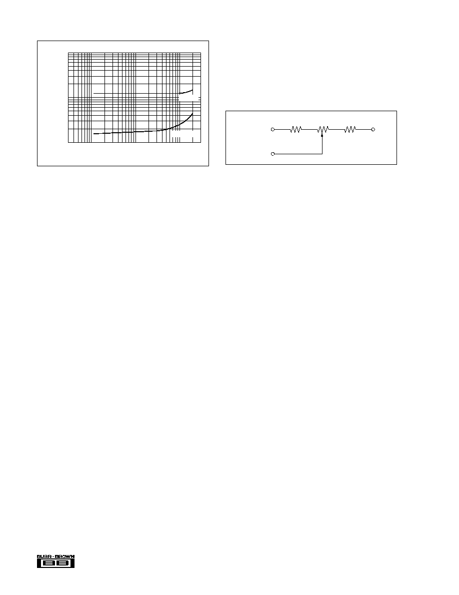
MSB ERROR ADJUSTMENT PROCEDURE
(OPTIONAL)
The MSB error of the PCM56 can be adjusted to make the
differential linearity error (DLE) at BPZ essentially zero.
This is important when the signal output levels are very low,
because zero crossing noise (DLE at BPZ) becomes very
significant when compared to the small code changes
occurring in the LSB portion of the converter.
Differential linearity error at bipolar zero and THD are
guaranteed to meet data sheet specifications without any
external adjustment. However, a provision has been made
for an optional adjustment of the MSB linearity point which
makes it possible to eliminate DLE error at BPZ. Two
procedures are given to allow either static or dynamic
adjustment. The dynamic procedure is preferred because of
the difficulty associated with the static method (accurately
measuring 16-bit LSB steps).
To statically adjust DLE at BPZ, refer to the circuit shown
in Figure 6, or the PCM56 connection diagram.
After allowing ample warm-up time (5-10 minutes) to assure
stable operation of the PCM56, select input code FFFF
hexadecimal (all bits on except the MSB). Measure the
audio output voltage using a 6-1/2 digit voltmeter and record
it. Change the digital input code to 0000 hexadecimal (all
bits off except the MSB). Adjust the 100k
potentiometer to
make the audio output read 92
µ
V more than the voltage
reading of the previous code (a 1LSB step = 92
µ
V).
A much simpler method is to dynamically adjust the DLE at
BPZ. Again, refer to Figure 6 for circuitry and component
values. Assuming the device has been installed in a digital
audio application circuit, send the appropriate digital input
to produce a ≠80dB level sinusoidal output. While measuring
the THD of the audio circuit output, adjust the 100k
potentiometer until a minimum level of distortion is observed.
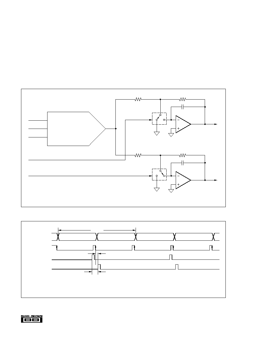
INPUT TIMING CONSIDERATIONS
Figure 7 and 8 refer to the input timing required to interface
the inputs of PCM56 to a serial input data stream. Serial data
is accepted in Binary Two's Complement (BTC) with the
MSB being loaded first. Data is clocked in on positive going
clock (CLK) edges and is latched into the DAC input
register on negative going latch enable (LE) edges.
The latch enable input must be high for at least one clock
cycle before going low, and then must be held low for at
least one clock cycle. The last 16 data bits clocked into the
serial input register are the ones that are transferred to the
DAC input register when latch enable goes low. In other
words, when more than 16 clock cycles occur between a
latch enable, only the data present during the last 16 clocks
will be transferred to the DAC input register.
One requirement for clocking in all 16 bits is the necessity
for a "17th" clock pulse. This automatically occurs when the
clock is continuous (last bit shifts in on the first bit of the
next data word). If the clock is stopped between input of 16-
bit data words, the latch enable (LE) must remain low until
after the first clock of the next 16-bit data word stream. This
ensures that the latch is properly set up.
Figure 7 refers to the general input format required for the
PCM56. Figure 8 shows the specific relationships between
the various signals and their timing constraints.
INSTALLATION
CONSIDERATIONS
If the optional external MSB error circuitry is used, a
potentiometer with adequate resolution and a TCR of 100ppm/
∞
C or less is required. Also, extra care must be taken to
insure that no leakage path (either AC or DC) exists to pin
14. If the circuit is not used, pins 14 and 15 should be left
open.
The PCM converter and the wiring to its connectors should
be located to provide the optimum isolation from sources of
RFI and EMI. The important consideration in the elimination
FIGURE 6. MSB Adjustment Circuit.
Frequency (Hz)
100
0.1
Total Harmonic Distortion (%)
0.01
0.001
1k
10k
20k
(Full Scale)
(≠20dB)
470k
100k
200k
Trim 15
MSB Adjust 14
1 ≠V
S

7
Æ
PCM56
FIGURE 7. Input Timing Diagram.
FIGURE 8. Input Timing Relationships.
source and drain of the FET switch operate at a virtual
ground when "C" and "B" are connected in the sample
mode, there is no increase in distortion caused by the
modulation effect of R
ON
by the audio signal.
Figure 10 shows the deglitcher controls for both left and
right channels which are produced by timing control logic.
A delay of 1.5
µ
s (t
) is provided to allow the output of the
PCM56 to settle within a small error band around its final
value before connecting it to the channel output. Due to the
fast settling time of the PCM56 it is possible to minimize the
delay between the left- and right-channel outputs when
using a single D/A converter for both channels. This is
important because the right- and left-channel data are recorded
in-phase and the use of the slower D/A converter would
result in significant phase error at higher frequencies.
The obvious solution to the phase shift problem in a two-
channel system would be to use two D/A converters (one per
channel) and time the outputs to change simultaneously.
Figure 11 shows a block diagram of the final test circuitry
used for PCM56. It should be noted that no deglitching
circuitry is required on the DAC output to meet specified
THD performance. This means that when one PCM56 is
used per channel, the need for all the sample/hold and
controls circuitry associated with a single DAC (two-channel)
design is effectively eliminated. The PCM56 is tested to
meet its THD specifications without the need for output
deglitching.
A low-pass filter is required after the PCM56 to remove all
unwanted frequency components caused by the sampling
frequency as well as those resulting from the discrete nature
of the D/A output. This filter must have a flat frequency
response over the entire audio band (0-20kHz) and a very
high attenuation above 20kHz.
Most previous digital audio circuits used a higher order (9-
13 pole) analog filter. However, the phase response of an
analog filter with these amplitude characteristics is nonlinear
and can disturb the pulse-shaped characteristic transients
contained in music.
of RF radiation or pickup is loop area; therefore, signal leads
and their return conductors should be kept close together.
This reduces the external magnetic field along with any
radiation. Also, if a signal lead and its return conductor are
wired close together, they represent a small flux-capture
cross section for any external field. This reduces radiation
pickup in the circuit.
APPLICATIONS
Figures 9 and 10 show a circuit and timing diagram for a
single PCM56 used to obtain both left- and right-channel
output in a typical digital audio system. The audio output of
the PCM56 is alternately time-shared between the left and
right channels. The design is greatly simplified because the
PCM56 is a complete D/A converter requiring no external
reference or output op amp.
A sample/hold (S/H) amplifier, or "deglitcher" is required at
the output of the D/A for both the left and right channel, as
shown in Figure 9. The S/H amplifier for the left channel is
composed of A
1
, SW
1
, and associated circuitry. A
1
is used
as an integrator to hold the analog voltage in C
1
. Since the
Data
Latch
Enable
2
(2)
Clock
(3)
MSB
LSB
MSB
(4)
(1)
NOTES: (1) If clock is stopped between input of 16-bit data words, latch enable (LE) must remain low until after the first clock of the next 16-bit data
word stream. (2) Data format is binary two's complement (BTC). Individual data bits are clocked in on the corresponding positive clock edge. (3) Latch
enable (LE) must remain low at least one clock cycle after going negative. (4) Latch enable (LE) must be high for at least one clock cycle before going
negative.
1
16
15
14
13
12
11
10
9
8
7
6
5
4
3
2
1
MSB
Data
Input
> 40ns
> One Clock Cycle
Latch
Enable
> One Clock Cycle
Clock
Input
> 40ns
> 5ns
> 100ns
> 15ns
LSB
>15ns >15ns
> 40ns
8
Æ
PCM56
SECOND GENERATION SYSTEMS
One method of avoiding the problems associated with a
higher order analog filter would be to use digital filter
oversampling techniques. Oversampling by a factor of two
would move the sampling frequency (88.2kHz) out to a
point where only a simple low-order phase-linear analog
filter is required after the deglitcher output to remove
unwanted intermodulation products. In a digital compact
disc application, various VLSI chips perform the functions
of error detection/correction, digital filtering, and formatting
of the digital information to provide the clock, latch enable,
and serial input to the PCM56. These VLSI chips are
available from several sources (Sony, Yamaha, Signetics,
etc.) and are specifically optimized for digital audio
applications.
Oversampled circuitry requires a very fast D/A converter
since the sampling frequency is multiplied by a factor of two
or more (for each output channel). A single PCM56 can
provide two-channel oversampling at a 4X rate (176.4kHz/
channel) and still remain well within the settling time
requirements for maintaining specified THD performance.
This would reduce the complexities of the analog filter even
further from that used in 2X oversampling circuitry.
FIGURE 9. A Sample/Hold Amplifier (Deglitcher) is Required at the Digital-to-Analog Output for Both Left and Right Channels.
FIGURE 10. Timing Diagram for the Deglitcher Control Signals.
R
2
2.2k
A
1
(1)
C
1
680pF
C
B
A
Left Channel
Output to LPF
SW
1
MP7512
(Micro Power)
R
4
2.2k
A
2
(1)
C
2
680pF
C
B
A
Right Channel
Output to LPF
SW
2
MP7512
(Micro Power)
R
1
2.2k
R
3
2.2k
NOTE: (1) 1 OPA101AM or 1/4 OPA404KP or 1 OPA606KP or OPA2604.
PCM56
Serial Data
Clock
Latch Enable
Left Channel
Deglitcher Control
Right Channel
Deglitcher Control
A "low" signal on the deglitcher control closes switch "A",
while a "high" signal closes switch "B".
Latch Enable
Right Channel
Serial Data
44.1kHz
Left Channel
Left Channel
Right Channel
Right Channel
Deglitcher Control
Left Channel
Deglitcher Control
t
DELAY
4.5µs max
t = 1.5µs DAC Settling Time
The deglitcher control signals by timing control logic. The fast settling time of the PCM56 makes it possible to
minimize the delay between left and right channels to about 4.5µs, which reduces phase error at the higher audio frequencies.

9
Æ
PCM56
The information provided herein is believed to be reliable; however, BURR-BROWN assumes no responsibility for inaccuracies or omissions. BURR-BROWN assumes
no responsibility for the use of this information, and all use of such information shall be entirely at the user's own risk. Prices and specifications are subject to change
without notice. No patent rights or licenses to any of the circuits described herein are implied or granted to any third party. BURR-BROWN does not authorize or warrant
any BURR-BROWN product for use in life support devices and/or systems.
FIGURE 11. Block Diagram of Distortion Test Circuit.
Distortion
Analyzer
(Shiba Soku Model
725 or Equivalent)
Programmable
Gain Amp
0dB to 60dB
Low-Pass
Filter
(Toko APQ-25
or Equivalent)
DUT
(PCM58P)
Parallel-to-Serial
Conversion
Digital Code
(EPROM)
Binary
Counter
Timing
Logic
Clock
Latch Enable
Sampling Rate = 44.1kHz x 4 (176.4kHz)
Output Frequency = 991Hz
Use 400Hz High-Pass
Filter and 30kHz
Low-Pass Filter
Meter Settings
LOW-PASS FILTER
CHARACTERISTIC
0
≠20
≠40
≠60
≠80
≠100
≠120
Gain (dB)
Frequency (Hz)
1
10 10 10 10 10
1
2
3
4
5