 | –≠–ª–µ–∫—Ç—Ä–æ–Ω–Ω—ã–π –∫–æ–º–ø–æ–Ω–µ–Ω—Ç: PCM58P | –°–∫–∞—á–∞—Ç—å:  PDF PDF  ZIP ZIP |
International Airport Industrial Park ∑ Mailing Address: PO Box 11400 ∑ Tucson, AZ 85734 ∑ Street Address: 6730 S. Tucson Blvd. ∑ Tucson, AZ 85706
Tel: (520) 746-1111 ∑ Twx: 910-952-1111 ∑ Cable: BBRCORP ∑ Telex: 066-6491 ∑ FAX: (520) 889-1510 ∑ Immediate Product Info: (800) 548-6132
DESCRIPTION
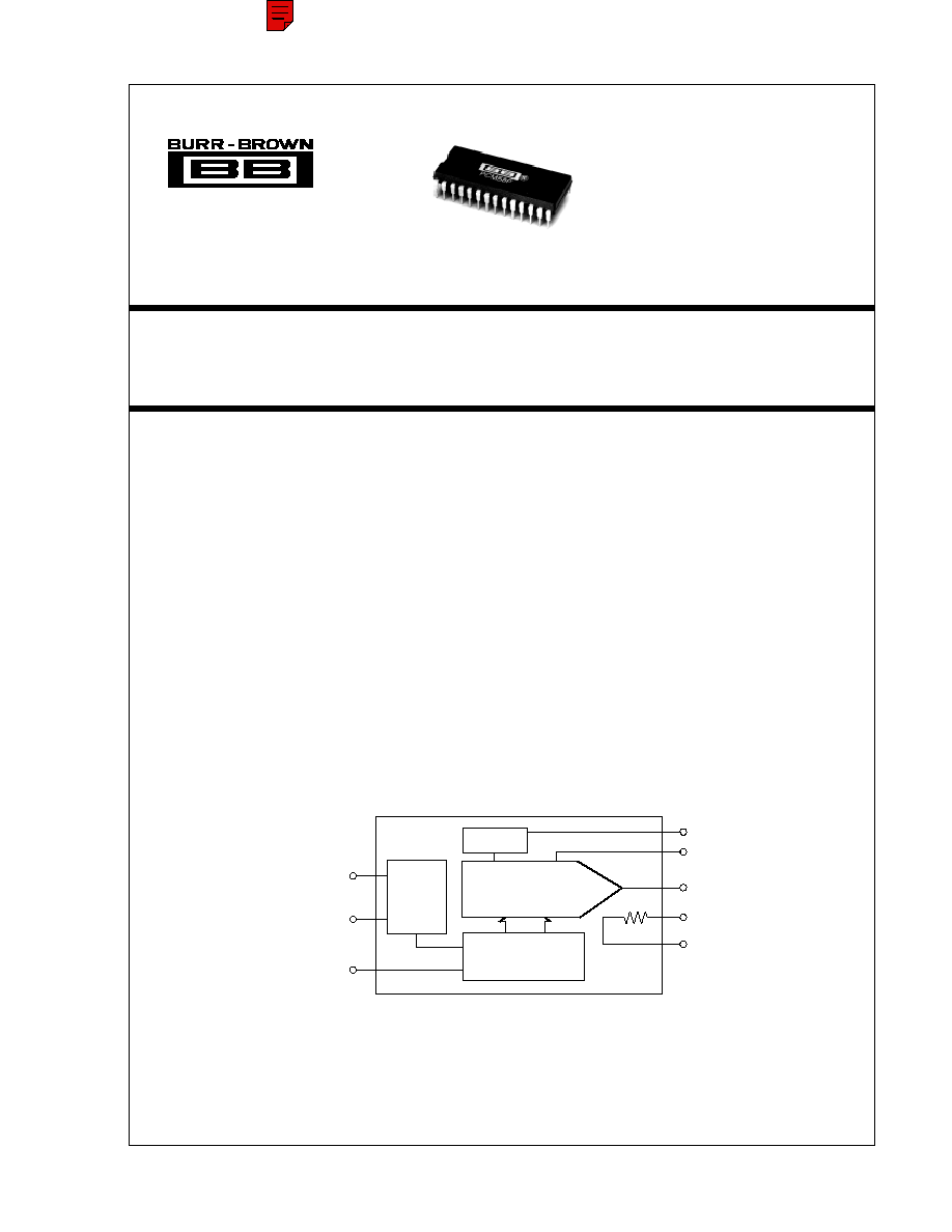
The PCM58P is a complete, precision 18-bit digital-
to-analog converter with ultra-low distortion over a very
wide frequency range. The latched serial input data
format of the PCM58P is totally based on the widely
successful 16-bit PCM56P format (with the addition of
two more data bits). The PCM58P features a very low
noise and fast settling current output.
The PCM58P comes in a 28-pin plastic DIP package.
A provision is made for external adjustment of the four
MSBs to further improve the PCM58P's specifications,
if desired. Applications include very low distortion
frequency synthesis and high-end consumer and pro-
fessional digital audio applications.
FEATURES
q
18-BIT MONOLITHIC AUDIO D/A
CONVERTER
q
VERY LOW MAX THD+N: ≠96dB Without
External Adjustment; PCM58P-K
q
SERIAL INPUT FORMAT 100%
COMPATIBLE WITH INDUSTRY STD
16-BIT PCM56P
q
VERY FAST SETTLING, GLITCH-FREE
CURRENT OUTPUT (200ns)
q
LOW-NOISE SCHMITT TRIGGER LOGIC
INPUT CIRCUITRY
q
COMPLETE WITH REFERENCE
q
RELIABLE PLASTIC 28-PIN DIP
PACKAGE
Precision, 18-Bit Monolithic Audio
DIGITAL-TO-ANALOG CONVERTER
PCM58P
PCM58P
18-Bit
I
OUT
DAC
Reference
Serial-to-Parallel
Shift Register
Clock
Latch Enable
Data
Control
Logic
V
REF
MSB Adj
I
OUT
R
F
R
F
Æ
©
1988 Burr-Brown Corporation
PDS-868A
Printed in U.S.A. October, 1993

PCM58P
Æ
2
SPECIFICATIONS
ELECTRICAL
All Specifications at 25
∞
C, and
±
V
CC
= +5.0V and ≠12.0V unless otherwise noted.
PCM58P /P,J/P,K
PARAMETER
CONDITIONS
MIN
TYP
MAX
UNITS
RESOLUTION
18
BITS
DYNAMIC RANGE
108
dB
DIGITAL INPUT
Logic Family
TTL/CMOS Compatible
Logic Level:
V
IH
+2.0
+V
CC
V
V
IL
0.0
0.8
V
I
IH
V
IH
= +2.7V
+1.0
µ
A
I
IL
V
IL
= +0.4V
≠50
µ
A
Data Format
Serial BTC
(1)
Input Clock Frequency
16.9
20
MHz
DYNAMIC CHARACTERISTICS
TOTAL HARMONIC DISTORTION + N
(2)
Without MSB Adjustments
PCM58P:
f = 991Hz (0dB)
(3)
f
S
= 176.4kHz
(4)
≠94
≠92
dB
f = 991Hz (≠20dB)
f
S
= 176.4kHz
≠74
≠72
dB
f = 991Hz (≠60dB)
f
S
= 176.4kHz
≠40
≠34
dB
PCM58P-J:
f = 991Hz (0dB)
f
S
= 176.4kHz
≠96
≠94
dB
f = 991Hz (≠20dB)
f
S
= 176.4kHz
≠80
≠74
dB
f = 991Hz (≠60dB)
f
S
= 176.4kHz
≠40
≠34
dB
PCM58P-K
f = 991Hz (0dB)
f
S
= 176.4kHz
≠100
≠96
dB
f = 991Hz (≠20dB)
f
S
= 176.4kHz
≠82
≠80
dB
f = 991Hz (≠60dB)
f
S
= 176.4kHz
≠42
≠40
dB
TRANSFER CHARACTERISTICS
ACCURACY
Gain Error
±
1
±
2
%
Bipolar Zero Error
(5)
±
10
mV
Gain Drift
0
∞
C to 70
∞
C
25
ppm/
∞
C
Bipolar Zero Drift
0
∞
C to 70
∞
C
4
ppm of FSR/
∞
C
Warm-up Time
1
Minute
IDLE CHANNEL SNR
(6)
20Hz to 20kHz at BPZ
(7)
+126
dB
POWER SUPPLY REJECTION
+72
dB
ANALOG OUTPUT
Output Range
±
0.98
±
1.0
±
1.02
mA
Output Impedance
1.2
k
Internal Feedback
3
k
Settling Time
1mA Step
200
ns
Glitch Energy
Meets all THD+N Specs Without External Deglitching
POWER SUPPLY REQUIREMENTS
+V
CC
Supply Voltage
+4.75
+5.00
+5.50
V
≠V
CC
Supply Voltage
≠10.8
≠12.0
≠13.2
V
Supply Current
+I
CC
+V
CC
= +5.0V
+10
mA
≠I
CC
≠V
CC
= ≠12.0V
≠30
mA
Power Dissipation
410
mW
TEMPERATURE RANGE
Specification
0
+70
∞
C
Operating
≠30
+70
∞
C
Storage
≠60
+100
∞
C
NOTES: (1) Binary Two's Complement coding. (2) Ratio of (Distortion
RMS
+ Noise
RMS
) / Signal
RMS
. (3) D/A converter output frequency/signal level. (4) D/A converter
sample frequency (4 x 44.1kHz; 4 times oversampling). (5) Offset error at bipolar zero. (6) Measured using an OPA27 and 10k
feedback and an A-weighted filter.
(7) Bipolar Zero.
The information provided herein is believed to be reliable; however, BURR-BROWN assumes no responsibility for inaccuracies or omissions. BURR-BROWN assumes
no responsibility for the use of this information, and all use of such information shall be entirely at the user's own risk. Prices and specifications are subject to change
without notice. No patent rights or licenses to any of the circuits described herein are implied or granted to any third party. BURR-BROWN does not authorize or warrant
any BURR-BROWN product for use in life support devices and/or systems.

Æ
PCM58P
3
PCM58P
-X
Basic Model Number
P: Plastic
Performance Grade Code
PIN
DESCRIPTION
MNEMONIC
P1
Decoupling Capacitor
CAP
P2
+Vcc Voltage Supply
+V
CC
P3
Decoupling Capacitor
CAP
P4
Decoupling Capacitor
CAP
P5
Bipolar Offset Point
BPO
P6
Current DAC I
OUT
I
OUT
P7
Feedback Resistor
R
F1
P8
Analog Common
ACOM
P9
≠V
CC
Voltage Supply
≠V
CC
P10
Feedback Resistor
R
F2
P11
Digital Common
DCOM
P12
No Connection
NC
P13
+V
CC
Voltage Supply
+V
CC
P14
No Connection
NC
P15
Decoupling Capacitor
CAP
P16
Clock
CLK
P17
DAC Latch Enable
LE
P18
No Connection
NC
P19
Data Input
DATA
P20
≠V
CC
Voltage Supply
≠V
CC
P21
No Connection
NC
P22
No Connection
NC
P23
No Connection
NC
P24
Bit 4 Adjust
B4 ADJ
P25
Bit 3 Adjust
B3 ADJ
P26
Bit 2 Adjust
B2 ADJ
P27
Bit 1 (MSB) Adjust
B1 ADJ
P28
Bit Adjust V
POT
V
POT
PIN ASSIGNMENTS
±
V
CC
Supply Voltages ................................................................ +6V; ≠16V
Input Logic Voltage ................................................................. ≠1V to +V
CC
Storage Temperature ...................................................... ≠60
∞
C to +100
∞
C
Lead Temperature (soldering, 10s) ................................................ +300
∞
C
ABSOLUTE MAXIMUM RATINGS
ORDERING INFORMATION
PACKAGE INFORMATION
(1)
PACKAGE DRAWING
MODEL
PACKAGE
NUMBER
PCM58P
28-Pin Plastic DIP
215
PCM58P, J
28-Pin Plastic DIP
215
PCM58P, K
28-Pin Plastic DIP
215
NOTE: (1) For detailed drawing and dimension table, please see end of data
sheet, or Appendix D of Burr-Brown IC Data Book.
FIGURE 1. PCM58P Production THD+N Test Setup.
DISCUSSION OF
SPECIFICATIONS
TOTAL HARMONIC DISTORTION + NOISE
The key specification for the PCM58P is total harmonic
distortion plus noise. Digital data words are read into the
PCM58P at four times the standard audio sampling frequency
of 44.1kHz or 176.4kHz such that a sinewave output of 991Hz
is realized. For production testing, the output of the DAC
goes to a programmable gain amplifier to provide gain at
lower signal output test levels and then through a 20kHz
low pass filter before being fed into an analog type distortion
analyzer. Figure 1 shows a block diagram of the production
THD+N test setup.
Programmable
Gain Amp
0dB to 60dB
Binary
Counter
Clock
0
≠20
≠40
≠60
≠80
≠100
≠120
Use 400Hz High-Pass
Filter and 30kHz
Low-Pass Filter
Meter Settings
(Shiba Soku Model
725 or Equivalent)
Digital Code
(EPROM)
Distortion
Analyzer
Parallel-to-Serial
Conversion
Timing
Logic
Sampling Rate = 44.1kHz X 4 (176.4kHz)
Output Frequency = 991Hz
Low-Pass
Filter
(Toko APQ-25
or Equivalent)
DUT
(PCM58P)
LOW-PASS FILTER
CHARACTERISTIC
Frequency (Hz)
Latch Enable
1 10
1
10
2
10
3
10
4
10
5
Gain (dB)

PCM58P
Æ
4
In terms of signal measurement, THD+N is the ratio of
Distortion
RMS
+ Noise
RMS
/ Signal
RMS
expressed in dB. For
the PCM58P, THD+N is 100% tested at three different output
levels using the test setup shown in Figure 1. It is significant
to note that this test setup does not include any output
deglitching circuitry. This means the PCM58P even meets
its ≠60dB THD+N specification without use of external
deglitchers.
ABSOLUTE LINEARITY
Even though absolute integral and differential linearity specs
are not given for the PCM58P, the extremely low THD+N
performance is typically indicative of 15-bit to 16-bit integral
linearity in the DAC depending on the grade specified. The
relationship between THD+N and linearity, however, is not
such that an absolute linearity specification for every indi-
vidual output code can be guaranteed.
IDLE CHANNEL SNR
Another appropriate spec for a digital audio converter is idle
channel signal-to-noise ratio (idle channel SNR). This is the
ratio of the noise on the DAC output at bipolar zero in relation
to the full scale range of the DAC. The output of the DAC
is band-limited from 20Hz to 20kHz and an A-weighted filter
is applied to make this measurement. The idle channel SNR
for the PCM58P is typically greater than +126dB, making
it ideal for low-noise applications.
OFFSET, GAIN, AND TEMPERATURE DRIFT
Although the PCM58P is primarily meant for use in dynamic
applications, specifications are also given for more traditional
DC parameters such as gain error, bipolar zero offset error,
and temperature gain drift and offset drift.
TIMING CONSIDERATIONS
The PCM58P accepts TTL-compatible logic input levels.
Noise immunity is enhanced by the use of Schmitt trigger
input architectures on all input signal lines. The data format
of the PCM58P is binary two's complement (BTC) with the
most significant bit (MSB) being first in the serial input bit
stream. Table I describes the exact input data to voltage output
coding relationship. Any number of bits can precede the 18
bits to be loaded as only the last 18 will be transferred to
the parallel DAC register after LE (P17; latch enable) has
gone low.
The individual DAC serial input data bit shifts transfer are
triggered on positive CLK edges. The serial to parallel data
transfer to the DAC occurs on the falling edge of LE (P17).
Refer to Figure 2 for graphical relationships of these signals.
MAXIMUM CLOCK RATE
The maximum clock rate of 16.9mHz for the PCM58P is
derived by multiplying the standard audio sample rate of
44.1kHz times sixteen (16X oversampling) times the standard
audio word bit length of 24 (44.1kHz x 16 x 24 = 16.9mHz).
Note that this clock rate accommodates a 24-bit word length,
even though only 18 bits are actually being used.
NOTES: (1) If clock is stopped between input of 18-bit data words, latch enable (LE) must remain low until after the first clock of the next 18-bit data word stream.
(2) Data format is binary two's complement (BTC). Individual data bits are clocked in on the corresponding positive clock edge. (3) Latch enable (LE) must
remain low at least one clock cycle after going negative. (4) Latch enable (LE) must be high for at least one clock cycle before going negative.
DIGITAL INPUT
ANALOG OUTPUT
Binary Two's
Voltage (V)
Current (mA)
Complement (BTC)
DAC Output
V
OUT
Mode
I
OUT
Mode
3FFFF Hex
+FS
+2.9999943
≠0.9999981
20000 Hex
BPZ
0.0000000
0.0000000
1FFFF Hex
BPZ ≠ 1LSB
≠0.0000057
+0.0000019
00000 Hex
≠FS
≠3.0000000
+1.0000000
TABLE I. PCM60P Input/Output Relationships.
FIGURE 2. PCM58P Timing Diagram.
P16 (Clock)
1
MSB
P18 (Data)
P17 (Latch Enable)
2
3
4
10
11
12
13
14
15
16
17
18
LSB
1
Æ
PCM58P
5
"STOPPED-CLOCK" OPERATION
The PCM58P is normally operated with a continuous clock
input signal. If the clock is to be stopped in between input
data words, the last 18-bits shifted in are not actually shifted
from the serial register to the latched parallel DAC register
until LE (latch enable) goes low. If the clock input (P16,
CLK) is stopped between data words, LE (P17) must remain
low until after the first clock cycle of the next data word
to insure proper DAC operation. In either case, the setup and
hold times for DATA and LE must still be observed as shown
in Figure 3.
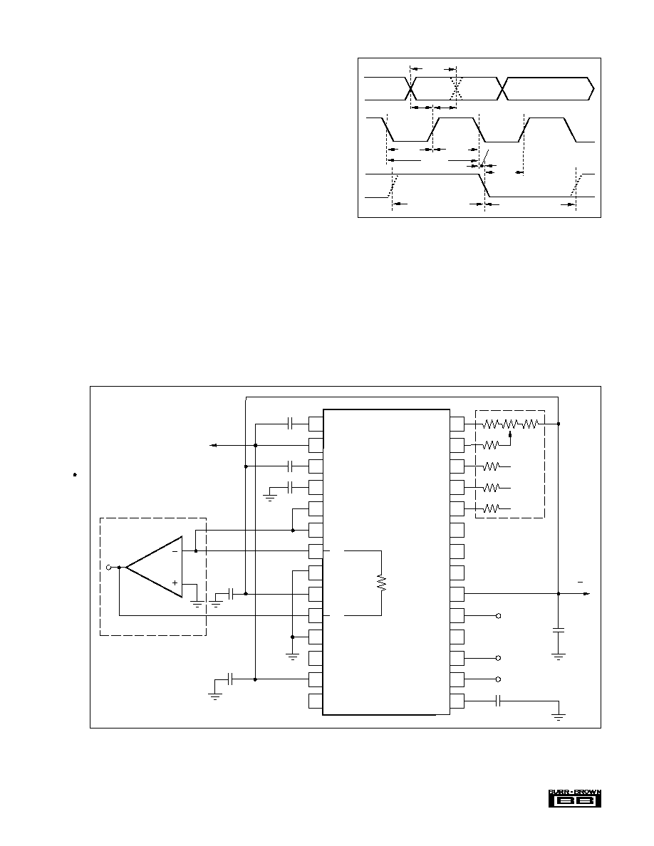
INSTALLATION
Refer to Figure 4 for proper connection of the PCM58P in
the voltage-out mode using the internal feedback resistor.
The feedback resistor connections (P7 and P10) should be
connected to ACOM (P8) if not used. The PCM58P requires
only a +5V and ≠12V supply. It is very important that these
supplies be as "clean" as possible to reduce coupling of supply
noise to the output. Power supply decoupling capacitors
shown in Figure 4 should be used, regardless of how good
the supplies are to maximize power supply rejection. All
grounds should be connected to the analog ground plane as
close to the PCM58P as possible.
FILTER CAPACITOR REQUIREMENTS
As shown in Figure 4, other various decoupling capacitors
are required around the supply and reference points with no
special tolerances being required. Placement of all capacitors
should be as close to the appropriate pins of the PCM58P
as possible to reduce noise pickup from surrounding circuitry.
FIGURE 4. PCM58P Connection Diagram.
FIGURE 3. PCM58P Setup and Hold Timing Diagram.
Data
Input
>40ns
LSB
MSB
>15ns >15ns
Clock
Input
>40ns
>40ns
>5ns
>100ns
>15ns
Latch
Enable
>One Clock Cycle
>One Clock Cycle
Optional External Op-Amp
Burr-Brown
OPA602BP
NOTE: Connect P7 and P10 to P8
(ACOM) if internal feedback resis-
tor is not used
Optional
Bit
Adjust
Circuit
3.3µF
3.3µF
0.1µF
0.1µF
0.1µF
+5V
CAP
+V
CC
CAP
CAP
BPO
I
OUT
R
F1
ACOM
≠V
CC
R
F2
DCOM
NC
+V
CC
NC
V
POT
Bit Adj (MSB)
Bit Adj (B2)
Bit Adj (B3)
Bit Adj (B4)
NC
NC
NC
≠V
CC
DATA
NC
LE
CLK
CAP
0.1µF
3.3µF
≠12V
330k
330k
330k
330k
100k
1k
1k
R
F
3k
+
+
+
+
+
+
+
28
27
26
25
24
23
22
21
20
19
18
17
16
15
1
2
3
4
5
6
7
8
9
10
11
12
13
14

PCM58P
Æ
6
MSB ADJUSTMENT CIRCUITRY
With the optional bit adjustment circuitry shown in Figure
4, even greater performance can be realized by reducing the
first four major bit carry output errors to zero. The most
important adjustment for low level outputs would be the step
between BPZ (bipolar zero; MSB on, all other bits off) and
the code, which is one LSB less than BPZ (MSB off, all
other bits on), since every crossing of zero would go through
this bipolar major carry point. This MSB bit adjustment would
be made by outputing a very low level signal sine wave and
calibrating the 100k
potentiometer circuit connected to P28
and P27 while monitoring the THD+N of the PCM58P until
peak performance is observed.
Bits 2 through 4 can also be adjusted if desired to obtain
optimum full-scale output THD+N performance. An addi-
tional 100k
potentiometer adjustment circuit is required for
every additional bit to be adjusted. If bit adjustment is not
performed, the respective pins on the PCM58P should be
left open.
Once bit adjustment is performed, the reference voltage at
VPOT (P28) will track the internal reference, insuring that
the THD+N performance of the PCM58P will remain unaf-
fected by external temperature changes.