 | –≠–ª–µ–∫—Ç—Ä–æ–Ω–Ω—ã–π –∫–æ–º–ø–æ–Ω–µ–Ω—Ç: PGA203 | –°–∫–∞—á–∞—Ç—å:  PDF PDF  ZIP ZIP |

Æ
PGA202/203
1
Covered by U.S. PATENT #4,883,422
PGA202/203
Æ
FEATURES
q
DIGITALLY PROGRAMMABLE GAINS:
DECADE MODEL--PGA202
GAINS OF 1, 10, 100, 1000
BINARY MODEL--PGA203
GAINS OF 1, 2, 4, 8
q
LOW BIAS CURRENT: 50pA max
q
FAST SETTLING: 2
µ
s to 0.01%
q
LOW NON-LINEARITY: 0.012% max
q
HIGH CMRR: 80dB min
q
NEW TRANSCONDUCTANCE CIRCUITRY
q
LOW COST
DESCRIPTION
The PGA202 is a monolithic instrumentation ampli-
fier with digitally controlled gains of 1, 10, 100, and
1000. The PGA203 provides gains of 1, 2, 4, and 8.
Both have TTL or CMOS-compatible inputs for easy
microprocessor interface. Both have FET inputs and a
new transconductance circuitry that keeps the band-
width nearly constant with gain. Gain and offsets are
laser trimmed to allow use without any external com-
ponents. Both amplifiers are available in ceramic or
plastic packages. The ceramic package is specified
over the full industrial temperature range while the
plastic package covers the commercial range.
International Airport Industrial Park ∑ Mailing Address: PO Box 11400 ∑ Tucson, AZ 85734 ∑ Street Address: 6730 S. Tucson Blvd. ∑ Tucson, AZ 85706
Tel: (520) 746-1111 ∑ Twx: 910-952-1111 ∑ Cable: BBRCORP ∑ Telex: 066-6491 ∑ FAX: (520) 889-1510 ∑ Immediate Product Info: (800) 548-6132
APPLICATIONS
q
DATA ACQUISITION SYSTEMS
q
AUTO-RANGING CIRCUITS
q
DYNAMIC RANGE EXPANSION
q
REMOTE INSTRUMENTATION
q
TEST EQUIPMENT
Digitally Controlled Programmable-Gain
INSTRUMENTATION AMPLIFIER
Front
End
and
Logic
Circuits
I
1
I
2
8
6
9
1
14
11
4
10
12
5
Filter B
≠
+
2
Adjust
+V
IN
A
0
A
1
Digital Common
Sense
V
OUT
V
REF
5.3pF*
5.3pF*
30k *
*±20%
30k *
V
OS
7
+V
IN
Filter A
©
1989 Burr-Brown Corporation
PDS-1006C
Printed in U.S.A. August, 1993

Æ
PGA202/203
2
* Same as the PGA202/203AG
NOTES: (1) All specifications apply to both the PGA202 and the PGA203. Values given for a gain of 10 are the same for a gain of 8 and other values may be interpolated.
(2) Measured with a 10k load. (3) The analog inputs are internally diode clamped. (4) Adjustable to zero. (5)
V
NOISE (RTI)
=
(V
N
INPUT
)
2
+ (V
N OUTPUT
/Gain)
2
.
(6) Threshold voltages are referenced to Digital Common. (7) From input change or gain change.
SPECIFICATIONS
ELECTRICAL
At +25
∞
C, V
CC
=
±
15V unless otherwise noted.
PGA202/203AG
(1)
PGA202/203BG
(1)
PGA202/203KP
(1)
PARAMETER
CONDITION
MIN
TYP
MAX
MIN
TYP
MAX
MIN
TYP
MAX
UNITS
GAIN
Error
(2)
G < 1000
0.05
0.25
*
0.15
*
*
%
G = 1000
0.1
1
0.08
0.5
*
*
%
Nonlinearity
G < 1000
0.002
0.015
*
0.012
*
*
%
G = 1000
0.02
0.06
*
0.04
*
*
%
Gain vs Temperature
G < 100
3
25
*
15
*
ppm/
∞
C
G = 100
40
120
*
60
*
ppm/
∞
C
G = 1000
100
300
*
150
*
ppm/
∞
C
RATED OUTPUT
Voltage
|I
OUT
|
5mA
±
10
±
12
*
*
*
*
V
Over Specified Temperature
See Typical Perf. Curve
±
9
*
±
10
V
Current
|V
OUT
|
10V
±
5
±
10
*
*
*
*
mA
Impedance
0.5
*
*
ANALOG INPUTS
Common-Mode Range
±
10
±
13
*
*
*
*
V
Absolute Max Voltage
(3)
No Damage
±
V
CC
*
*
V
Impedance, Differential
10 || 3
*
*
G
|| pF
Common-Mode
10 || 1
*
*
G
|| pF
OFFSET VOLTAGE (RTI)
Initial Offset at 25
∞
C
(4)
±
(0.5 +
±
(2 +
*
±
(1 +
*
*
mV
5/G)
24/G)
12/G)
vs Temperature
±
(3 +
±
(24 +
*
±
(12 +
*
µ
V/
∞
C
50/G)
240/G)
120/G)
Offset vs Time
50
*
*
µ
V/Month
Offset vs Supply
10
V
CC
15
10 +
100 +
*
50 +
*
*
µ
V/V
250/G
900/G
450/G
INPUT BIAS CURRENT
Initial Bias Current: at 25
∞
C
10
50
*
*
*
*
pA
at 85
∞
C
640
3200
*
*
*
*
pA
Initial Offset Current: at 25
∞
C
5
25
*
*
*
*
pA
at 85
∞
C
320
1600
*
*
*
*
pA
COMMON-MODE REJECTION RATIO
G = 1
80
100
*
*
*
*
dB
G = 10
86
110
*
*
*
*
dB
G = 100
92
120
*
*
*
*
dB
G = 1000
94
120
*
*
*
*
dB
INPUT NOISE
Noise Voltage 0.1 to 10Hz
1.7
*
*
µ
Vp-p
Noise Density at 10kHz
(5)
12
*
*
nV/
Hz
OUTPUT NOISE
Noise Voltage 0.1 to 10Hz
32
*
*
µ
Vp-p
Density at 1kHz
(5)
400
*
*
nV/
Hz
DYNAMIC RESPONSE
Frequency Response
G < 1000
1000
*
*
kHz
G = 1000
250
*
*
kHz
Full Power Bandwidth
G < 1000
400
*
*
kHz
G = 1000
100
*
*
kHz
Slew Rate
10
20
15
*
*
*
V/
µ
s
Settling Time (0.01%)
(7)
G < 1000
2
*
*
µ
s
G = 1000
10
*
*
µ
s
Overload Recovery Time
(7)
G < 1000
5
*
*
µ
s
G = 1000
10
*
*
µ
s
DIGITAL INPUTS
Digital Common Range
≠V
CC
V
CC
≠ 8
*
*
*
*
V
Input Low Threshold
(6)
0.8
*
*
V
Input Low Current
10
*
*
µ
A
Input High Voltage
2.4
*
*
V
Input High Current
10
*
*
µ
A
POWER SUPPLY
Rated Voltage
±
15
*
*
V
Voltage Range
±
6
±
18
*
*
*
*
V
Quiescent Current
6.5
*
*
mA
TEMPERATURE RANGE
Specification
≠25
85
*
*
0
70
∞
C
Operating
≠55
125
*
*
≠25
85
∞
C
Storage
≠65
150
*
*
≠40
100
∞
C
JA
100
*
*
∞
C/W

Æ
PGA202/203
3
ABSOLUTE MAXIMUM RATINGS
PIN CONFIGURATION
Supply Voltage ...................................................................................
±
18V
Internal Power Dissipation ............................................................. 750mW
Analog and Digital Inputs .....................................................
±
(V
CC
+ 0.5V)
Operating Temperature Range:
G Package ............................................................... ≠55
∞
C to +125
∞
C
P Package ............................................................... ≠40
∞
C to +100
∞
C
Lead Temperature (soldering, 10s) .................................................. 300
∞
C
Output Short Circuit Duration ................................................... Continuous
Junction Temperature ...................................................................... 175
∞
C
PACKAGE INFORMATION
PACKAGE DRAWING
MODEL
PACKAGE
NUMBER
(1)
PGA202KP
14-Pin Plastic DIP
010
PGA202AG
14-Pin Ceramic DIP
169
PGA202BG
14-Pin Ceramic DIP
169
PGA203KP
14-Pin Plastic DIP
010
PGA203AG
14-Pin Ceramic DIP
169
PGA203BG
14-Pin Ceramic DIP
169
NOTE: (1) For detailed drawing and dimension table, please see end of data
sheet, or Appendix D of Burr-Brown IC Data Book.
Top View
DIP
The information provided herein is believed to be reliable; however, BURR-BROWN assumes no responsibility for inaccuracies or omissions. BURR-BROWN assumes
no responsibility for the use of this information, and all use of such information shall be entirely at the user's own risk. Prices and specifications are subject to change
without notice. No patent rights or licenses to any of the circuits described herein are implied or granted to any third party. BURR-BROWN does not authorize or warrant
any BURR-BROWN product for use in life support devices and/or systems.
TEMPERATURE
OFFSET VOLTAGE
MODEL
GAINS
PACKAGE
RANGE
MAX (mV)
PGA202KP
1, 10, 100, 1000
Plastic DIP
0
∞
C to +70
∞
C
±
(2 + 24/G)
PGA202AG
1, 10, 100, 1000
Ceramic DIP
≠25
∞
C to +85
∞
C
±
(2 + 24/G)
PGA202BG
1, 10, 100, 1000
Ceramic DIP
≠25
∞
C to +85
∞
C
±
(1 + 12/G)
PGA203KP
1, 2, 4, 8
Plastic DIP
0
∞
C to +70
∞
C
±
(2 + 24/G)
PGA203AG
1, 2, 4, 8
Ceramic DIP
≠25
∞
C to +85
∞
C
±
(2 + 24/G)
PGA203BG
1, 2, 4, 8
Ceramic DIP
≠25
∞
C to +85
∞
C
±
(1 + 12/G)
ORDERING INFORMATION
14 Digital Common
13 ≠V
12 V
11 V Sense
10 Filter B
9 V Adjust
8 +V
CC
OUT
OUT
OS
IN
A 1
A 2
+V 3
V 4
Filter A 5
V Adjust 6
≠V 7
CC
REF
OS
IN
1
0
Æ
PGA202/203
4
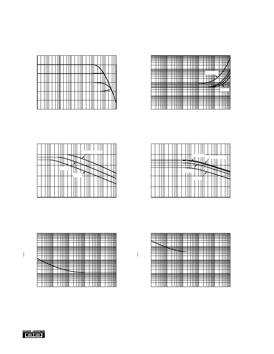
OUTPUT NOISE vs FREQUENCY
1
10
10
2
10
3
10
10
4
5
Frequency (Hz)
Noise (nV/
Hz)
10
1
10
2
10
3
10
4
INPUT NOISE vs FREQUENCY
1
10
10
2
10
3
10
10
4
5
Frequency (Hz)
Noise (nV/
Hz)
10
1
10
2
10
3
10
4
1
10
10
2
10
3
10
10
10
6
4
5
Frequency (Hz)
PSRR (dB)
PSRR vs FREQUENCY
160
120
80
40
0
≠40
G = 1000
G = 100
G = 10
G = 1
GAIN ERROR vs FREQUENCY
1
10
10
2
10
3
10
10
4
5
Frequency (Hz)
Gain Error (%)
10
1
10
≠1
10
≠2
10
≠3
G = 1000
G = 1
80
60
40
20
0
≠20
≠40
1
10
10
2
10
3
10
10
10
6
10
7
4
5
Frequency (Hz)
Gain (dB)
GAIN vs FREQUENCY
TYPICAL PERFORMANCE CURVES
T
A
= +25
∞
C, V
S
=
±
15V unless otherwise noted.
1
10
10
2
10
3
10
10
10
6
4
5
Frequency (Hz)
CMRR (dB)
CMRR vs FREQUENCY
160
120
80
40
0
≠40
G = 100, 1000
G = 10
G = 1

Æ
PGA202/203
5
0
20
Filter Capacitor (pF)
Settling Time (µs)
SETTLING TIME vs FILTER CAPACITOR
10
8
6
4
2
≠4
10
30
1000
500
0
1500
2000
15
10
5
0
V (V)
Load ( )
OUTPUT SWING vs LOAD
OUT
12
9
6
15
18
15
10
5
0
V (V)
Power Supply (±V)
OUTPUT SWING vs POWER SUPPLY
OUT
T = +25∞C
A
T = ≠25∞C
A
12
9
6
15
18
16
12
8
4
0
V (V)
Power Supply (±V)
INPUT RANGE vs POWER SUPPLY
IN
12
9
6
15
18
12
11
10
9
8
0
Input Bias Current (pA)
Power Supply (±V)
INPUT BIAS CURRENT vs POWER SUPPLY
7
QUIESCENT CURRENT vs POWER SUPPLY
12
9
6
15
18
10
8
6
4
2
0
I (mA)
Power Supply (±V)
Q
TYPICAL PERFORMANCE CURVES
(CONT)
T
A
= +25
∞
C, V
S
=
±
15V unless otherwise noted.