 | –≠–ª–µ–∫—Ç—Ä–æ–Ω–Ω—ã–π –∫–æ–º–ø–æ–Ω–µ–Ω—Ç: PWS725A | –°–∫–∞—á–∞—Ç—å:  PDF PDF  ZIP ZIP |
1
Æ
PWS725A/726A
PWS725A
PWS726A
Isolated, Unregulated
DC/DC CONVERTERS
International Airport Industrial Park ∑ Mailing Address: PO Box 11400 ∑ Tucson, AZ 85734 ∑ Street Address: 6730 S. Tucson Blvd. ∑ Tucson, AZ 85706
Tel: (520) 746-1111 ∑ Twx: 910-952-1111 ∑ Cable: BBRCORP ∑ Telex: 066-6491 ∑ FAX: (520) 889-1510 ∑ Immediate Product Info: (800) 548-6132
FEATURES
q
ISOLATED
±
7 TO
±
18VDC OUTPUT FROM
SINGLE 7 TO 18VDC SUPPLY
q
±
15mA OUTPUT AT RATED VOLTAGE
ACCURACY
q
HIGH ISOLATION VOLTAGE
PWS725A, 1500Vrms
PWS726A, 3500Vrms
q
LOW LEAKAGE CAPACITANCE: 9pF
q
LOW LEAKAGE CURRENT: 2
µ
A max,
at 240VAC 50/60Hz
q
HIGH RELIABILITY DESIGN
q
AVAILABLE WITH OUTPUT
SYNCHRONIZATION SIGNAL FOR USE
WITH ISO120 AND ISO121
oscillator before either MOSFET driver turns on,
protects the switches, and eliminates high inrush cur-
rents during turn-on. Input current sensing protects
both the converter and the load from possible thermal
damage during a fault condition.
Special design features make these converters
especially easy to apply. The compact size allows
dense circuit layout while maintaining critical isola-
tion requirements. The Input Sync connection allows
frequency synchronization of multiple converters. The
Output Sync is available to synchronize ISO120 and
ISO121 isolation amplifiers. The Enable input allows
control over output power in instances where
shutdown is desired to conserve power, such as in
battery-powered equipment, or where sequencing of
power turn-on/turn-off is desired.
DESCRIPTION
The PWS725A and PWS726A convert a single 7 to
18VDC input to bipolar voltages of the same value as
the input voltage. The converters are capable of
providing
±
15mA at rated voltage accuracy and up to
±
40mA without damage. (See Output Current Rating.)
The PWS725A and PWS726A converters provide
reliable, engineered solutions where isolated power is
required in critical applications. The high isolation
voltage rating is achieved through use of a specially-
designed transformer and physical spacing. An addi-
tional high dielectric-strength, low leakage transformer
coating increases the isolation rating of the PWS726A.
Reliability and performance are designed in. The
bifilar wound, wirebonded transformer simultaneously
provides lower output ripple than competing designs,
and a higher performance/cost ratio. The soft-start
oscillator/driver design assures full operation of the
q
PROTECTED AGAINST OUTPUT FAULTS
q
COMPACT
q
LOW COST
q
EASY TO APPLY--FEW EXTERNAL PARTS
APPLICATIONS
q
MEDICAL EQUIPMENT
q
INDUSTRIAL PROCESS EQUIPMENT
q
TEST EQUIPMENT
q
DATA ACQUISITION
© 1987 Burr-Brown Corporation
PDS-736D
Printed in U.S.A. October, 1993

2
Æ
PWS725A/726A
PARAMETER
CONDITIONS
MIN
TYP
MAX
MIN
TYP
MAX
UNITS
INPUT
Rated Voltage
15
*
VDC
Input Voltage Range
7
18
*
*
VDC
Input Current
I
O
=
±
15mA
77
*
mA
Input Current Ripple
No External Filtering
150
*
mAp-p
L-C Input Filter, L
IN
= 100
µ
H, C
IN
= 1
µ
F
(1)
5
*
mAp-p
C Only, C
IN
= 1
µ
F
60
mAp-p
ISOLATION
Test Voltages
Input to Output, 10 seconds
4000
8000
VDC
Input to Output, 60 seconds, min
1500
3500
Vrms
Rated Voltage
Input to Output, Continuous, AC 60Hz
1500
3500
Vrms
Input to Output, Continuous DC
2121
4950
VDC
Isolation Impedance
Input to Output
10
12
|| 9
*
|| pF
Leakage Current
Input to Output, 240Vrms, 60Hz
1.2
2.0
*
*
µ
A
OUTPUT
Rated Output Voltage
14.25
15
15.75
*
*
*
VDC
Output Current
Balanced Loads
15
40
*
*
mA
Single-Ended
80
*
mA
Load Regulation
Balanced Loads,
±
10mA < I
OUT
<
±
40mA
0.4
*
%/mA
Ripple Voltage (400kHz)
No External Capacitor
60
*
mVp-p
L
O
= 10
µ
H, C
O
= 1
µ
F (Figure 1)
10
*
mVp-p
L
O
= 0
µ
H, C
O
Filter Only
Output Switching Noise
L
O
= 10
µ
H, C
O
= 1
µ
F
1
*
mVp-p
Output Capacitive Load
L
O
= 100
µ
H, C Filter
10
*
µ
F
C Filter Only
1
*
µ
F
Voltage Balance, V+, V≠
0.04
%
Sensitivity to
V
IN
1.15
V/V
Output Voltage Temp. Coefficient
10
mV/
∞
C
Output Sync Signal
Square Wave, 50% Duty Cycle
30
*
Vp-p
TEMPERATURE
Specification
≠25
+85
*
*
∞
C
Operating
≠25
+85
*
*
∞
C
Storage
≠25
+125
*
*
∞
C
SPECIFICATIONS
ELECTRICAL
T
A
= +25
∞
C, C
L
= 1
µ
F ceramic, V
IN
= 15VDC, operating frequency = 800kHz, V
OUT
=
±
15VDC, C
IN
= 1
µ
F ceramic, I
OUT
=
±
15mA, unless otherwise specified.
PSW726A
PWS725A
* Specification same as PWS725A.
See Performance Curves
The information provided herein is believed to be reliable; however, BURR-BROWN assumes no responsibility for inaccuracies or omissions. BURR-BROWN assumes
no responsibility for the use of this information, and all use of such information shall be entirely at the user's own risk. Prices and specifications are subject to change
without notice. No patent rights or licenses to any of the circuits described herein are implied or granted to any third party. BURR-BROWN does not authorize or warrant
any BURR-BROWN product for use in life support devices and/or systems.
PIN CONFIGURATION
PACKAGE INFORMATION
(1)
PACKAGE DRAWING
MODEL
PACKAGE
NUMBER
PWS725A
32-Pin Ceramic DIP
210
PWS726A
32-Pin Ceramic DIP
210
NOTE: (1) For detailed drawing and dimension table, please see end of data
sheet, or Appendix D of Burr-Brown IC Data Book.
Top View
DIP
+V
O
NC
Output Ground
Output Sync
Frequency Adjust
Frequency Adjust
Enable
NC
≠V
O
NC
NC
Output Ground
NC
Input Ground
Input Sync
V
IN
32
31
30
29
20
19
18
17
1
2
3
4
13
14
15
16

3
Æ
PWS725A/726A
LOAD REGULATION
Output Voltage (V)
10
0
20
18
16
14
12
Balanced Loads
10
20
30
40
Output Current (mA)
20
40
60
80
Balanced
Single
Single-ended Loads
V
IN
= +15V
OUTPUT VOLTAGE DRIFT
Temperature (∞C)
Output Voltage (%)
≠6
≠50
100
0
50
0
≠1
≠2
≠3
≠4
≠5
85
TYPICAL PERFORMANCE CURVES
T
A
= +25
∞
C, V
CC
=
±
15VDC unless otherwise noted.
Capacitance (µF)
OUTPUT CAPACITANCE vs RIPPLE VOLTAGE
Output Ripple Voltage (mVp-p)
0
0
1
0.3
100
90
80
70
60
50
40
30
20
10
0.1
0.2
0.4
0.5
0.6
0.7
0.8
0.9
Peak-to-Peak
Capacitor Only
DC
<
f
<
20MHz
L-C Filter, L = 100µH
I
O
= ±15mA
V
IN
= ±15V
MAXIMUM POWER DISSIPATION
Temperature (∞C)
Output Power (W)
0
≠25
2
1
0
25
50
75
100
85
1.44
LINE REGULATION
Input Voltage (V)
Output Voltage (V)
4
6
20
18
16
14
12
10
8
6
8
10
12
14
16
18
I
O
= ±15mA
7
INPUT CURRENT vs OUTPUT CURRENT
I
O
(mA)
I
IN
(mA)
0
0
140
70
±15
±30
±45
77

4
Æ
PWS725A/726A
TYPICAL PERFORMANCE CURVES
(CONT)
T
A
= +25
∞
C, V
CC
=
±
15VDC unless otherwise noted.
THEORY OF OPERATION
The PWS725A and the PWS726A DC/DC converters con-
sist of a free-running oscillator, control and switch driver
circuitry, MOSFET switches, a transformer, a bridge recti-
fier, and filter capacitors together in a 32-pin DIP (0.900
inches nominal) package. The control circuitry consists of
current limiting, soft start, frequency adjust, enable, and
synchronization features. See Figure 1. In instances where
several converters are used in a system, beat frequencies
developed between the converters are a potential source of
low frequency noise in the supply and ground paths. This
noise may couple into signal paths. See Figures 2 and 3 for
connection of INPUT SYNC pin. Converters can be syn-
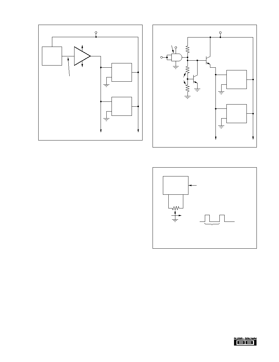
FIGURE 1. PWS725A/726A Functional Diagram.
chronized and these beat frequencies avoided. The unit with
the highest natural frequency will determine the synchro-
nized running frequency. To avoid excess stray capaci-
tance, the INPUT SYNC pin should not be loaded with
more than 50pF. If unused, the INPUT SYNC must be left
open.
Soft start circuitry protects the MOSFET switches during
start up. This is accomplished by holding the gate-to-source
voltage of both MOSFET switches low until the free-
running oscillator is fully operational. In addition to that
soft start circuitry, input current sensing also protects the
MOSFET switches. This current limiting keeps the FET
Full-Wave
Bridge
Rectifier
Load
Load
Oscillator/
Driver
Control
R
SC
20
19
20k
18
15
14
16
L
IN
(5)
V
IN
7-18/VDC
C
IN
(5)
Frequence
Increase
(1)
ENABLE
(3)
INPUT
SYNC
(2)
0.22µF
0.22µF
0.22µF
L
O
(4)
L
O
(4)
32
1
4 & 30
C
O
(4)
C
O
(4)
+
≠
+
≠
+V
OUT
≠V
OUT
+I
O
≠I
O
29
OUTPUT SYNC
(1) Frequency Adjust is optional, with pins 19 and 20 left open. The normal switching frequency is 800kHz.
(2) Leave INPUT SYNC pin open if unused; limit stray capacitance on INPUT SYNC pin to less than 50pF.
(3) Leave ENABLE pin open or connect to V
IN
if not used.
(4) Optional output filtering, with L
O
= 0, limit C
O
1µF, with L
O
= 100µH, limit C
O
10µF, see Performance
Curves for L
O
= 0.
(5) Optional input filtering, see Performance Curves for L
IN
= 0.
(6) CAUTION: Do not connect pin 29 to low impedance loads. See Figure 5.
NOTES:
SYNC FREQUENCY vs
INPUT CURRENT AND OUTPUT VOLTAGE
SYNC Frequency (kHz)
(Optional External Control)
Output Voltage (V)
400
15
14
800
1200
1600
90
80
70
60
Input Current (mA)
V
IN
= +15V
±V
OUT
I
INPUT
(I
O
= ±15mA)
5
Æ
PWS725A/726A
FIGURE 2. Synchronization of Multiple PWS725As or
PWS726As from a Master Converter.
FIGURE 3. Synchronization of Multiple PWS725As or
PWS726As from an External TTL Signal.
FIGURE 4. Frequency Adjustment Procedure.
OUTPUT CURRENT RATING
The total current which can be drawn from the PWS725A
or PWS726A is a function of total power being drawn from
both outputs (see Functional Diagram). If one output is not
used, then maximum current can be drawn from the other
output. If both outputs are loaded, the total current must be
limited such that:
|I
L
+| + |I
L
≠|
80mA
It should be noted that many analog circuit functions do not
simultaneously draw full rated current from both the posi-
tive and negatives supplies. For example, an operational
amplifier may draw 13mA from the positive supply under
16
PWS725A/726A
15
19
(1)
+7V to +18 V
16
PWS725A/726A
15
19
(1)
To Other
PWS725A/726A
Converters
NOTES: (1) Units to be synchronized
should have a lower free-running
frequency than the TTL signal.
Grounding Frequency Adjust (Pin 19)
will shift the free-running frequency
to approximately 400kHz. (2) The TTL
SYNC signal can have a frequency
range of 450kHz to 1.5MHz.
2N3904
2N3904
3
8
4
1
2
TTL
SYNC
Signal
(2)
MC1472
or Equivalent
Peripheral
Driver
620
100
1/8W
+5V
330
1W
15
20
PWS725A/726A
19
20k
(1)
Frequency
Increase
Monitor frequency with scope
or frequency counter (use
low C probe).
+5V
BE
+4V
BE
1.25µs Nominal
SYNC Signal
NOTE: (1) For nominal 800kHz operation, leave
pins 19 and 20 open.
15
4
16
Master
PWS725A
Buffer
≠V
CC
+V
CC
OPA633
8
Keep Connection
Short
16
Slave
PWS725A/726A
15
19
(1)
+7V to +18 V
16
15
19
(1)
To Other
PWS725A/726A
Converters
NOTE: (1) Units to be synchronized
should have a lower free-running
frequency than the master unit.
Grounding Frequency Adjust (pin 19)
will shift the free-running frequency
to approximately 400kHz.
Slave
PWS725A/726A
switches operating in their safe operating area under fault
conditions or excessive loads. When either of these condi-
tions occur, the peak input current exceeds a safe limit. The
result is an approximate 5% duty cycle, 300
µ
s drive period
to the MOSFET switches. This protects the internal MOSFET
switches as well as the external load from any thermal
damage. When the fault or excessive load is removed, the
converter resumes normal operation. A delay period of
approximately 50
µ
s incorporated in the current sensing
circuitry allows the output filter capacitors to fully charge
after a fault is removed. This delay period corresponds to a
filter capacitance of no more than 1
µ
F at either of the output
pins. This provides full protection of the MOSFET switches
and also sufficiently filters the output ripple voltage (see
specification table). The current sensing circuitry is de-
signed to provide thermal protection for the MOSFET
switches over the operating temperature range as well. The
low thermal resistance for the package (
JC
= 10
∞
C/W)
ensures safe operation under rated conditions. When these
rated conditions are exceeded, the unit will go into its
shutdown mode.
An optional potentiometer can be connected between the
two FREQUENCY ADJUST pins to trim the oscillator
operating frequency
±
10% (see Figure 4). Care should be
taken when trimming the frequency near the low frequency
range. If the frequency is trimmed too low, the peak induc-
tive currents in the primary will trip the input current
sensing circuitry to protect the MOSFET switches from
these peak inductive currents.
The ENABLE pin allows external control of output power.
When this pin is pulled low, output power is disabled. Logic
thresholds are TTL compatible. When not used, the Enable
input may be left open or tied to V
IN
(pin 16).

6
Æ
PWS725A/726A
full load while drawing only 3mA from the negative supply.
Under these conditions, the PWS725A/726A could supply
power for up to five devices (80mA
˜
16mA
5). Thus, the
PWS725A/726A can power more circuits than is at first
apparent.
ISOLATION VOLTAGE RATINGS
Because a long-term test is impractical in a manufacturing
situation, the generally accepted practice is to perform a
production test at a higher voltage for some shorter period of
time. The relationship between actual test conditions and the
continuous derated maximum specification is an important
one. Burr-Brown has chosen a deliberately conservative
one: VDC
TEST
= (2 X VACrms
CONTINUOUS RATING
) + 1000V for
ten seconds. This choice is appropriate for conditions where
system transient voltages are not well defined.
(1)
Where the
real voltages are well-defined or where the isolation voltage
is not continuous, the user may choose a less conservative
derating to establish a specification from the test voltage.
OUTPUT SYNC SIGNAL
To allow synchronization of an ISO120 or ISO121 isolation
amplifier, the PWS725A and PWS726A have an OUTPUT
SYNC signal at pin 29. It should be connected as shown in
Figure 5 to keep capacitive loading of pin 29 to a minimum.
If output sync is not used, leave pin open.
FIGURE 5. Synchronization with ISO120 or ISO121 Isola-
tion Amplifier.
29
PWS725A/726A
20k
4
20pF
Ext Osc
Connection
of
ISO120
or
ISO121
NOTE: (1) Reference National Electrical Manufacturers Association (NEMA)
Standards Parts ICS I-109 and ICS I-111.