 | –≠–ª–µ–∫—Ç—Ä–æ–Ω–Ω—ã–π –∫–æ–º–ø–æ–Ω–µ–Ω—Ç: PWS740 | –°–∫–∞—á–∞—Ç—å:  PDF PDF  ZIP ZIP |

Æ
PWS740
1
PWS740
Distributed Multi-Channel Isolated
DC-TO-DC CONVERTER
FEATURES
q
ISOLATED
±
7 TO
±
20VDC OUTPUTS
q
BARRIER 100% TESTED AT 1500VAC, 60Hz
q
LOWEST POSSIBLE COST PER CHANNEL
q
MINIMUM PC BOARD SPACE
q
80% EFFICIENCY (8 CHANNELS, RATED
LOADS)
q
FLEXIBLE USE WITH PWS745
COMPONENTS
APPLICATIONS
q
INDUSTRIAL MEASUREMENT AND
CONTROL
q
DATA ACQUISITION SYSTEMS
q
TEST EQUIPMENT
DESCRIPTION
The PWS740 is a multichannel, isolated DC-to-DC
converter with a 1500VAC continuous isolation rat-
ing. The outputs track the input voltage to the con-
verter over the range of 7 to 20VDC. The converter's
modular design, comprising three components, mini-
mizes the cost of isolated multichannel power for the
user.
The PWS740-1 is a high-frequency (400kHz nominal)
oscillator/driver, handling up to eight channels. This
part is a hybrid containing an oscillator and two power
FETs. It is supplied in a TO-3 case to provide the
power dissipation necessary at full load. Transformer
impedance limits the maximum input current to about
700mA at 15V input, well within the unit's thermal
limits. A TTL-compatible ENABLE pin provides out-
put shut-down if desired. A SYNC pin allows syn-
chronization of several PWS740-1s.
The PWS740-2 is a trifilar-wound isolation trans-
former using a ferrite core and is encapsulated in a
plastic package, allowing a higher isolation voltage
rating. One PWS740-2 is used per isolated channel.
Æ
© 1987 Burr-Brown Corporation
PDS-758H
Printed in U.S.A. January, 1998
International Airport Industrial Park ∑ Mailing Address: PO Box 11400, Tucson, AZ 85734 ∑ Street Address: 6730 S. Tucson Blvd., Tucson, AZ 85706 ∑ Tel: (520) 746-1111 ∑ Twx: 910-952-1111
Internet: http://www.burr-brown.com/ ∑ FAXLine: (800) 548-6133 (US/Canada Only) ∑ Cable: BBRCORP ∑ Telex: 066-6491 ∑ FAX: (520) 889-1510 ∑ Immediate Product Info: (800) 548-6132
Up to
6 More
Channels
Freq
Adj
20µH
Oscillator/
Driver
1
2
6
5
4
0.3µF
* Optional features; if unused, leave open.
** User Option
0.3µF
V
DRIVE
*7
*2
*1
PWS740-1
3
8
5
6
4
10µF
V+
PWS740-2
T
O
O
T
2
6
5
4
3
1
3
0.3µF
BAV99
Functional Diagram
BAV99
0.3µF
10µH
10µH
+V
O
Gnd1
≠V
O
0.3µF
BAV99
BAV99
0.3µF
10µH
10µH
+V
O
Gnd1
≠V
O
PWS740

2
Æ
PWS740
SPECIFICATIONS
ELECTRICAL
At V
IN
= 15V, output load on each of 8 channels =
±
15mA, T
A
= +25
∞
C, unless otherwise specified.
PARAMETER
CONDITION
MIN
TYP
MAX
UNITS
PWS740 SYSTEM
ISOLATION
Rated Voltage
Continuous, AC, 50/60Hz
1500
VACrms
Continuous, DC
2121
VDC
Test Voltage
10s, minimum
4000
VACrms
Impedance
Measured from Pin 2 to Pin 5 of the PWS740-2
10
12
|| 3
|| pF
Leakage Current
240VACrms, 60Hz Per Channel
0.5
1.5
µ
A
INPUT
Rated Voltage
15
VDC
Voltage Range
7
20
VDC
Current
±
30mA Output Load on 8 Channels, V
IN
= 15V
520
mA
Rated Output Load on 8 Channels, V
IN
= 15V
300
mA
Current Ripple
Full Output Load on 8 Channels, V
IN
= 15V with
Filter on Input
1
mA
OUTPUT
Rated Voltage
±
15mA Output Load on 8 Channels
14
15
16
VDC
Voltage at Min Load
±
1mA/Channel
30
VDC
Voltage Range
±
15mA Output Load on Each Channel
±
7
±
20
VDC
V
OUT
vs Temp
±
15mA Output Load on Each Channel
±
0.05
V/
∞
C
Load Regulation
±
3mA < Output Load <
±
30mA
0.25
V/mA
Tracking Regulation
V
OUT
/V
IN
1.2
V/V
Ripple Voltage
See Typical Performance Curves
Noise Voltage
See Theory of Operation
Current | +I
OUT
| + | ≠I
OUT
|
Each Channel
60
mA
TEMPERATURE
Specification
≠25
+85
∞
C
Operation
≠25
+85
∞
C
PWS740-1 OSCILLATOR/DRIVER
Frequency
V
IN
= 15V
350
400
470
kHz
Supply
7
15
20
V
Enable
Drivers On
2
V
S
V
Drivers Off
0
0.8
V
PWS740-2 ISOLATION TRANSFORMER
Isolation Test Voltage
10s, minimum
4000
VACrms
60s, minimum
1500
VACrms
Rated Isolation Voltage
Continuous
1500
VACrms
Isolation Impedance
10
12
|| 3
|| pF
Isolation Leakage
240VAC
0.5
1.5
µ
A
Primary Inductance
400kHz, Pin 1 to Pin 5
300
µ
H
Winding Ratio
Primary/Secondary
68/76
DIODE BRIDGE SPECIFICATIONS
Reverse Recovery
I
F
= I
R
= 50mA
40
ns
Reverse Breakdown
I
R
= 100
µ
A
55
V
Reverse Current
V
R
= 40V
1.5
µ
A
Forward Voltage
I
F
= 100mA
1.8
V
The information provided herein is believed to be reliable; however, BURR-BROWN assumes no responsibility for inaccuracies or omissions. BURR-BROWN assumes
no responsibility for the use of this information, and all use of such information shall be entirely at the user's own risk. Prices and specifications are subject to change
without notice. No patent rights or licenses to any of the circuits described herein are implied or granted to any third party. BURR-BROWN does not authorize or warrant
any BURR-BROWN product for use in life support devices and/or systems.

Æ
PWS740
3
PIN CONFIGURATION
Top Views
PACKAGE INFORMATION
PACKAGE DRAWING
PRODUCT
PACKAGE
NUMBER
(1)
PWS740-1 Driver
TO-3
030
PWS740-2 Transformer
6-Pin Plastic DIP
216
NOTE: (1) For detailed drawing and dimension table, please see end of data
sheet, or Appendix C of Burr-Brown IC Data Book.
2
3
4
5
6
7
8
1
PWS740-1
Enable
+V
IN
Freq Adj
Sync
Gnd
T
O
Return
T
AC
Gnd
AC
T
V
T
1
2
3
4
5
6
O
D
O
O
Plastic DIP
PWS740-2
TO-3
(Drawings Not to Scale)
ELECTROSTATIC
DISCHARGE SENSITIVITY
This integrated circuit can be damaged by ESD. Burr-Brown
recommends that all integrated circuits be handled with
appropriate precautions. Failure to observe proper handling
and installation procedures can cause damage.
ESD damage can range from subtle performance degradation
to complete device failure. Precision integrated circuits may
be more susceptible to damage because very small parametric
changes could cause the device not to meet its published
specifications.
4
Æ
PWS740
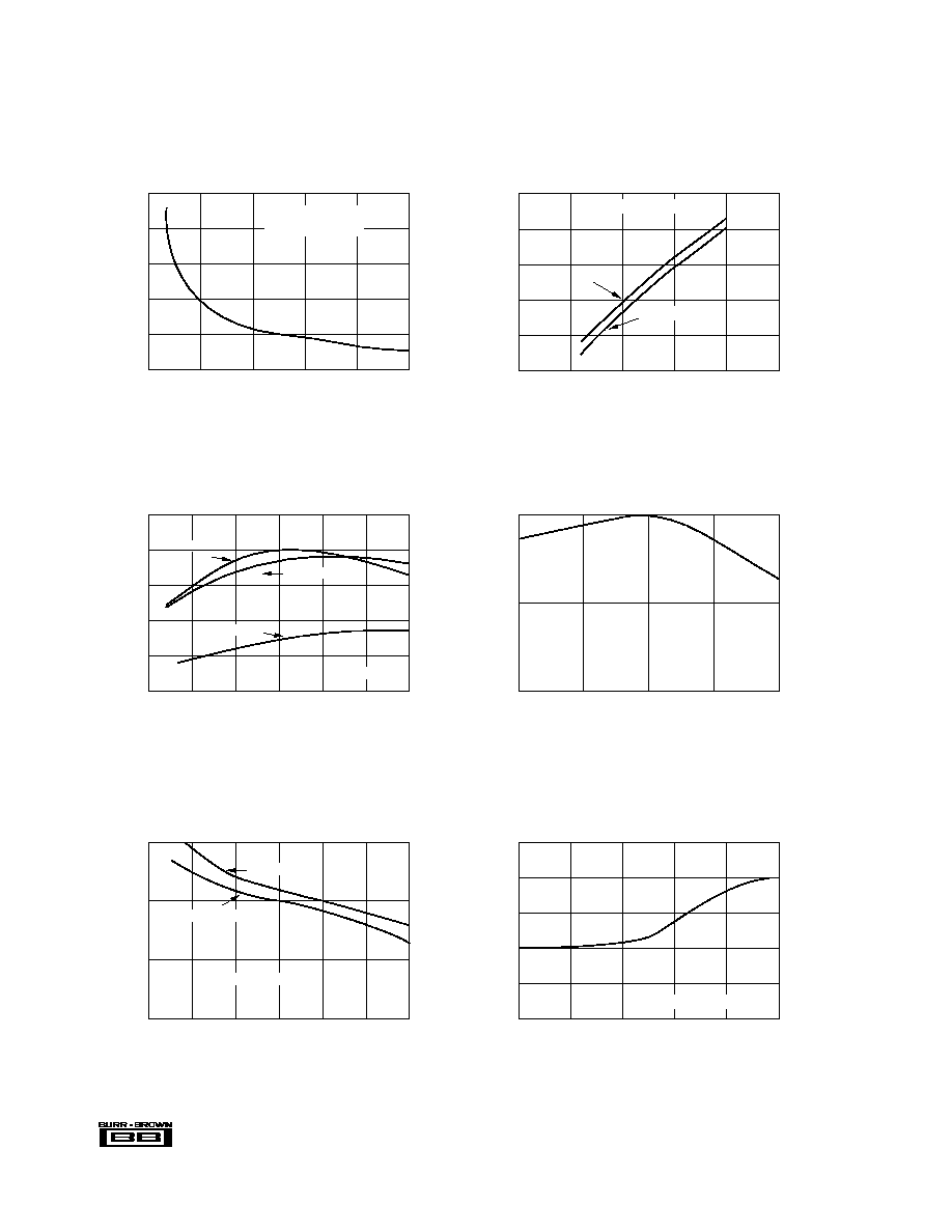
TYPICAL PERFORMANCE CURVES
V vs C
C (µF)
0
0.2
0.4
0.6
0.8
1.0
25
20
15
10
5
0
V (mVp-p)
LOAD
RIPPLE
RIPPLE
LOAD
V
IN
= 15V
I
O
= ±15mA/Channel
1 THROUGH 8 CHANNELS
V (V)
0
5
10
15
20
25
25
20
15
10
5
0
±V (V)
LINE REGULATION
1 channel
±I = ±15mA/Channel
O
IN
OUT
4 or 8 channels
EFFICIENCY vs LOAD 1,4, AND 8 CHANNELS
±I (mA)
0
100
80
60
40
20
0
Efficiency (%)
OUT
5
10
15
20
25
30
IN
4 Channels
V = +15V
8 Channels
1 Channel
OUTPUT VOLTAGE DRIFT
Temperature (∞C)
≠25
0
≠5
≠10
Rated V (%)
+50
+85
OUT
0
+25
LOAD REGULATION 1, 4 AND 8 CHANNELS
±I (mA)
0
20
15
10
5
±V
OUT
5
10
15
20
25
30
OUT
IN
4 and 8 Channel
V = 15V
1 Channel
FREQUENCY ADJUSTMENT RANGE
Frequency Adjustment Resistor ( )
1
10
100
1k
10k
100k
500
400
300
200
100
0
PWS740-1 Operating Frequency (kHz)
See Functional Diagram

Æ
PWS740
5
PIN DESCRIPTIONS OF
PWS740-1 DRIVER
+V
IN
, RETURN, AND GND
These are the power supply pins. The ground connection,
RETURN, for the N-channel MOSFET sources is brought
out separately from the ground connection for the oscillator/
driver chip. The waveform of the FETs' ground return
current (and also the current in the V
DRIVE
line) is an 800kHz
sawtooth. A capacitor between +V
IN
and the FET ground
provides a bypass for the AC portion of this current.
The power should never be instantaneously interrupted to
the PWS740 system (i.e., a break in the line from V+, either
accidental or by means of a series switch). Normal power-
down of the V+ supply is not considered instantaneous.
Should a rapid break in input power occur, however, the
transformers' voltage will rapidly increase to maintain cur-
rent flow. Such a voltage spike may damage the PWS740-1.
The bypass capacitors at the +V
IN
pin of the PWS740-1 and
the V
DRIVE
pins of the transformers provide a path for the
primary current if power is interrupted; however, total pro-
tection requires some type of bidirectional 1A voltage clamp-
ing at the +V
IN
pin. A low cost SA20A TransZorb
Æ
from
General Semiconductor
(1)
or equivalent, which will clamp
the +V
IN
pin between ≠0.6V and +23V, is recommended.
T
O
AND T
O
These pins are the drains of the N-channel MOSFET switches
which drive all the transformer primaries in parallel. The
signals on these pins are 400kHz complementary square
waves with twice the amplitude of the voltage at +V
IN
. It is
these lines that allow the power to be distributed to the
individual high voltage isolation transformers. Without proper
printed circuit board layout techniques, these lines could
generate interference to analog circuits. See the next section
on PCB layout.
ENABLE
A high TTL logic level on this pin activates the MOSFET
driver circuitry. A low TTL level applied to the ENABLE
pin shuts down all drive to the transformers and the output
voltages go to zero (only the oscillator is unaffected). For
continuous operation, the ENABLE pin can be left open or
tied to a voltage between +2V and +V.
SYNCHRONIZATION
The SYNC pin is used to synchronize up to eight PWS740-
1 oscillators. Synchronization is useful to prevent beat fre-
quencies in the supply voltages. The SYNC pins of two or
more PWS740-1s are tied together to force all units to the
same frequency of oscillation. The resultant frequency is
slightly higher than that of the highest unsynchronized unit.
If this feature is not required, leave the SYNC pin open. The
SYNC pin is sensitive to capacitance loading. 150pF or less
is recommended. Also external parasitic capacitive feedback
between either T
O
and the SYNC pin can cause unstable
operation (commonly seen as jitter in the T
O
outputs). Keep
SYNC connections and T
O
lines as physically isolated as
possible. Avoid shorting the SYNC pin directly to ground or
supply potentials; otherwise, damage may result.
Figure 1 shows a method for synchronizing a greater number
of PWS740-1 drivers. One unit is chosen as the master. Its
synchronization signal, buffered by a high-speed unity gain
amplifier can synchronize up to 20 slave units. Pin 1 of each
slave unit must be grounded to assure synchronization.
Minimize capacitive coupling between the buffered sync
line and the outputs of the drivers, especially at the end of
long lines. Capacitance to ground is not critical, but total
stray capacitance between the sync line and switching out-
puts should be kept below 50pF. Where extreme line lengths
are needed, such as between printed circuit boards, addi-
tional OPA633 buffers may be added to keep drive imped-
ance at an acceptably low value. Because of temperature-
influenced shifts in the switching levels, best operation of
this circuit will occur when differences in ambient tempera-
tures between the PWS740-1 drivers are minimized, typi-
cally within a 35
∞
C range.
(1) General Semiconductor Industries Inc., 2001 W. 10th Place, Tempe AZ 85281,
602-968-3101.
TransZorb
Æ
General Semiconductor Industries Inc.
FIGURE 1. Master/Slave Synchronization of Multiple
PWS740 Drivers.
OPA633
6
8 Channels
4
Typical at
25∞C
200ns
400kHz
8 Channels
8 Channels
NC
1
2
3.0V
2.5V
1
1
Slave
740-1
#1
Slave
740-1
#20
4
2
6
4
2
6
Master
740-1
+15V
≠15V