 | –≠–ª–µ–∫—Ç—Ä–æ–Ω–Ω—ã–π –∫–æ–º–ø–æ–Ω–µ–Ω—Ç: PWS750-4U | –°–∫–∞—á–∞—Ç—å:  PDF PDF  ZIP ZIP |

Æ
PWS750
1
PWS750-3U
PWS750-2U
4
3
4
1
6
3
2
5
6
7
0.3µF
0.3µF
10
≠V
O
+V
O
S
D
G
S
D
G
2N7002
or
2N7008
2N7002
or
2N7008
0.3µF
Driver
Soft
Start
Oscillator
R
1
T
16
T
0.3µF
Comparator
Differential
Amplifier
+V
+V
IN
7
3
11
10µH
PWS750-1U
TTL
OUT
TTL
IN
Enable
V
D
Input
Gnd
12
14
10
(2)
(2)
(1)
10
(1)
10
(3)
10
(3)
Reference
S
(1)
Output
Ground
The PWS750-2U and PWS750-4U are split-bobbin
wound isolation transformers using a ferrite core.
They are encapsulated in plastic packages, allowing a
high isolation voltage rating.
The PWS750-3U is a high-speed monolithic diode
bridge in a plastic 8-pin SO package.
One PWS750-1U can be used to drive up to four
channels (15V nominal operation). One PWS750-2U
and PWS750-3U and two 2N7002 (surface mount) or
2N7008 (TO-92) MOSFETs made by Siliconix are
used per isolated channel. When a PWS750-4U is
used as the transformer (5V input), then two TN0604s
made by Supertex must be used, due to the higher
currents of the primary (lower RDS on) and the lower
V
GS
threshold. With 5V operation only one channel
can be directly driven by the PWS750-1U (a simple
FET booster circuit can be used for multichannel
operation; see Figure 3).
Isolated, Unregulated
DC/DC CONVERTER COMPONENTS
PWS750
DESCRIPTION
The PWS750 consists of three building blocks for
building a low cost DC/DC converter. With them you
can optimize DC/DC converter PC board layout or
build a multichannel isolated DC/DC converter. All
parts are surface mount, requiring minimal space to
build the converter. The modular design minimizes the
cost of isolated power.
The PWS750-1U is a high-frequency (800kHz nomi-
nal) driver that can drive N-channel MOSFETs up to
the size of a 1.3A 2N7010. The recommended
MOSFET for individual transformer drivers is the
2N7008. The PWS750-1U is supplied in a 16-pin
double-wide SO package.
APPLICATIONS
q
INDUSTRIAL PROCESS CONTROL
EQUIPMENT
q
GROUND-LOOP ELIMINATION
q
PC-BASED DATA ACQUISITION
q
VENDING MACHINES
FEATURES
q
100% TESTED FOR HIGH-VOLTAGE
BREAKDOWN
q
COMPACT-SURFACE MOUNT
q
MULTICHANNEL OPERATION
q
5V OR 15V INPUT OPTIONS
q
FLEXIBLE USE WITH PWS740/PWS745
COMPONENTS
PWS750 SINGLE-CHANNEL CONNECTION
Typical Connection for
Internal Oscillator Operation
NOTES: (1) User option. (2) Use TN0604 for 5V to
±
15V operation. (3) Multichannel Operation.
Duplicate for multichannel
operation with PWS750-2U.
Æ
©
1988 Burr-Brown Corporation
PDS-838F
Printed in U.S.A. April, 1997
International Airport Industrial Park ∑ Mailing Address: PO Box 11400, Tucson, AZ 85734 ∑ Street Address: 6730 S. Tucson Blvd., Tucson, AZ 85706 ∑ Tel: (520) 746-1111 ∑ Twx: 910-952-1111
Internet: http://www.burr-brown.com/ ∑ FAXLine: (800) 548-6133 (US/Canada Only) ∑ Cable: BBRCORP ∑ Telex: 066-6491 ∑ FAX: (520) 889-1510 ∑ Immediate Product Info: (800) 548-6132

2
Æ
PWS750
SPECIFICATIONS
ELECTRICAL
At T
A
= 25
∞
C; +V
IN
= +15V; and I
OUT
=
±
15mA balanced loads, unless otherwise noted.
PARAMETER
CONDITIONS
MIN
TYP
MAX
UNITS
PWS750-1U OSCILLATOR
Frequency: Internal OSC
TTL
IN
= 0V
725
800
875
kHz
External OSC
1
2.5
MHz
Supply: 15V Operation
10
15
18
V
5V Operation
4.5
5
5.5
V
T, T Drive Current
50
mApk
T, T Drive Voltage, High
3
7
V
Low
0.7
V
TTL
IN
, I
IH
10
nA
I
IL
≠1
µ
A
V
IH
2
V
V
IL
0.8
V
TTL
OUT
, I
OL
15
mA
PWS750-2U +V
IN
TO
±
V
OUT
ISOLATION TRANSFORMER
ISOLATION
Voltage Rated Continuous AC 60Hz
750
Vrms
100% Test
(1)
60Hz, 1s, <5pC PD
1200
Vrms
Barrier Impedance
10
12
|| 8
|| pF
Leakage Current at 60Hz
V
ISO
= 240Vrms
1
1.5
µ
Arms
Winding Ratio
Primary/Secondary
48/48
PWS750-3U DIODE BRIDGE
Reverse Recovery
I
F
= I
R
= 50mA
40
ns
Reverse Breakdown
I
R
= 100
µ
A
55
V
Reverse Current
V
R
= 40V
1.5
µ
A
Forward Voltage
I
F
= 100mA
1.8
V
PWS750-4U +5V
IN
to
±
15V
OUT
ISOLATION TRANSFORMER
ISOLATION
Voltage Rated Continuous AC 60Hz
750
Vrms
100% Test
(1)
60Hz, 1s, <5pC PD
1200
Vrms
Barrier Impedance
10
12
|| 8
|| pF
Leakage Current at 60Hz
V
ISO
= 240Vrms
1
1.5
µ
Arms
Winding Ratio
Primary/Secondary
24/70
TEMPERATURE RANGE
Specification
0
+70
∞
C
Operating
Derated performance
≠40
+85
∞
C
Storage
≠40
+85
∞
C
NOTES: (1) Tested at 1.6
x
rated, fail on 5pC partial discharge leakage current on five successive pulses at 60Hz.
The information provided herein is believed to be reliable; however, BURR-BROWN assumes no responsibility for inaccuracies or omissions. BURR-BROWN assumes
no responsibility for the use of this information, and all use of such information shall be entirely at the user's own risk. Prices and specifications are subject to change
without notice. No patent rights or licenses to any of the circuits described herein are implied or granted to any third party. BURR-BROWN does not authorize or warrant
any BURR-BROWN product for use in life support devices and/or systems.

Æ
PWS750
3
8
7
6
4
3
2
1
14
5
T
V
D
+V
IN
16
15
13
12
11
10
9
16-Pin SO Double-Wide
Surface Mount
Enable
Gnd
TTL
OUT
TTL
IN
T
PWS750-1U
PIN CONFIGURATIONS
AC
4
3
2
1
5
6
7
8
AC
+V
≠V
8-Pin SO
Surface Mount
PWS750-3U
5
PWS750-2U
PWS750-4U
8-Pin DIP
Surface Mount
6
8
7
1
2
3
4
NC
AC
Gnd
AC
NC
T
O
V
D
T
O
ABSOLUTE MAXIMUM RATINGS
Supply Voltage ..................................................................................... 18V
Junction Temperature ...................................................................... 150
∞
C
Storage Temperature ........................................................ ≠40
∞
C to +85
∞
C
Lead temperature (soldering, SOIC, 3s) ........................................ +260
∞
C
Max Load, Sum of Both Outputs (PWS750-2U, 4U) ......................... 60mA
PWS750-XU
Basic Model Number
Components
1U : High-Frequency Driver
2U, 4U : Isolation Transformer
3U : High-Speed Monolithic Diode Bridge
ORDERING INFORMATION
PACKAGE INFORMATION
PACKAGE DRAWING
PRODUCT
PACKAGE
NUMBER
(1)
PWS750-1U
16-Pin SOIC
211
PWS750-2U
8-Pin Plastic
226
PWS750-3U
8-Pin SO
182
PWS750-4U
8-Pin Plastic
226
NOTE: (1) For detailed drawing and dimension table, please see end of data
sheet, or Appendix C of Burr-Brown IC Data Book.

4
Æ
PWS750
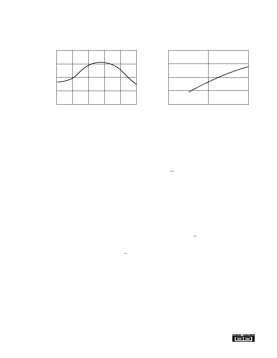
TYPICAL PERFORMANCE CURVES
T
A
= +25
∞
C, V
IN
= 15VDC, I
LOAD
=
±
15mA unless otherwise noted.
PWS750-4U LINE REGULATION
5.3
5.2
5.1
5
4.9
4.8
4.7
14
15
16
17
±V (V)
OUT
Input (V)
4.6
5.4
13
18
PWR750-2U LINE REGULATION
16
14
12
10
10
12
14
16
±V (V)
OUT
Input (V)
18
18
PWR750-2U AND PWS70-4U LOAD LINES
10
15
20
0
5
10
15
20
25
30
±V (V)
OUT
Load (mA)
PWS750-2U
PWS750-4U
OUTPUT RIPPLE VOLTAGE
50
40
30
20
10
0
0.2
0.4
0.6
0.8
1
Filter Capacitance (µF)
Ripple Voltage (mVp-p)
Ripple Frequency =
Oscillator Frequency
0.1
EFFICIENCY/LOAD CURVE
80
70
60
50
40
30
0
5
10
15
20
25
30
Efficiency (%)
PWS750-4U
4 Channel
PWS750-1U
PWS750-2U
Load Current (±mA)
TTL SIGNAL DUTY CYCLE
IN
100
75
50
25
0
% Duty Cycle
1
1.5
2
2.5
Synchronization Frequency (MHz)
(= Twice the FET Drive Frequency)
DC = %
t
H
t + t
H L
t
H
t
L
Acceptable
Duty
Cycle
Nominal Operating
Frequency
Synchronization Frequency (MHz)
(= Twice the FET Drive Frequency)
Æ
PWS750
5
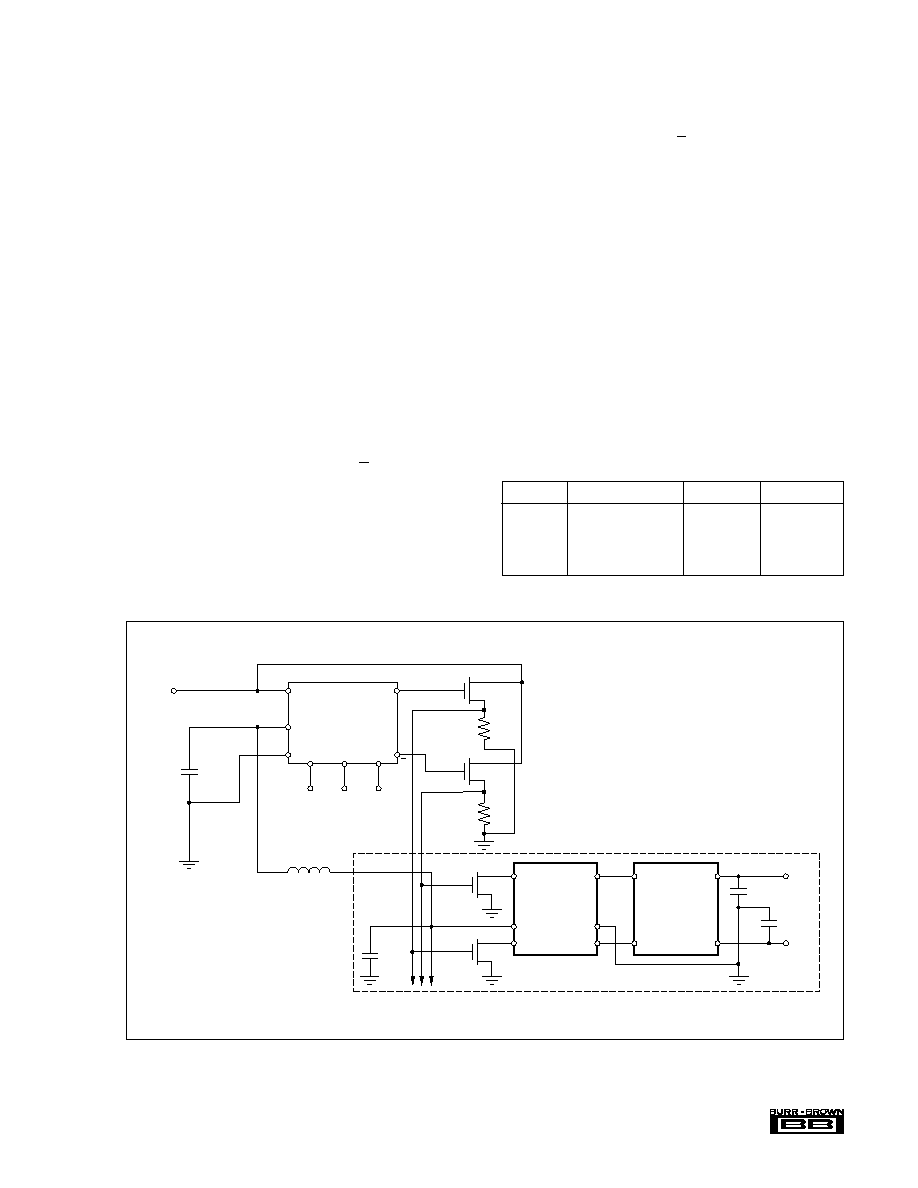
THEORY OF OPERATION
The PWS750 components are basic building blocks to be
used with other standard components to build an isolated
push-pull DC/DC converter. The oscillator runs at 800kHz
nominal, making it possible to reduce the size of the trans-
former and lower the output ripple voltage.
PWS750-1U OSCILLATOR PIN FUNCTIONS
TTL
IN
is used to control the driver frequency with an
external TTL level frequency source. The input frequency
must be twice the desired driver frequency, since there is an
internal divide-by-2 circuit to produce a 50% duty cycle
output. The input duty cycle can vary from 12% to 95% (see
Typical Performance Curves). When in the free running
mode, the TTL
IN
pin must be tied to ground.
TTL
OUT
is used when it is desired to synchronize the outputs
of multiple PWS750-1Us to minimize beat frequency prob-
lems. A standard open collector output is provided, therefore
a 330
to 3.3k
pull-up resistor will be necessary depend-
ing on stray capacitance on the sync line. A maximum of
eight PWS750-1Us can be connected without the use of an
external TTL buffer.
An Enable pin is provided so that the driver (T, T) can be
shut down to minimize power use if required. A TTL low
applied to the pin will shut down the driver within one cycle.
A TTL high will enable the driver within one cycle. The
TTL
OUT
will still have an 800kHz signal when a master
driver is disabled, so other synchronized drivers will not be
shut down. The pin can be left open for normal operation.
The +V
IN
pin supplies power to the oscillator. The V
D
pin
connects the power to the transformer through the internal
overcurrent sense resistor. The other end of the overcurrent
sense resistor is tied to +V
IN
. A 0.3
µ
F bypass capacitor must
be connected to the V
D
pin to reduce the ripple current
through the shunt resistor; otherwise false current limit
conditions can occur due to ripple voltage peaks.
TYPICAL PERFORMANCE CURVES
(CONT)
T
A
= +25
∞
C, V
IN
= 15VDC, I
LOAD
=
±
15mA unless otherwise noted.
During overload conditions the output drive shuts off for
approximately 80
µ
s, then turns back on for 20
µ
s, resulting
in a 25% power up duty cycle. If the overload condition still
exists, then the output will shut off again. When the fault or
the excessive load is removed, the converter resumes normal
operation.
The T and T pins are the complementary FET drive outputs
and are tied directly to the corresponding FET gate. The
connection must be as short as possible. For multiple chan-
nel operation they cannot be located above any ground or
power planes, because capacitive loading will not allow fast
enough charging of the FET gate.
PWS750-2U AND PWS750-4U
TRANSFORMER PIN FUNCTIONS
On the primary side the V
D
pin of the PWS750-2U is tied
directly to the V
D
pin of the PWS750-1U. Remember to
place a 0.1
µ
F capacitor as close to the PWS750-2U V
D
pin
as possible. The T
O
and T
O
pins are connected to the drains
of the corresponding FETs, whose sources are connected to
ground. On the secondary side of the transformer, the Gnd
pin is tied directly to the isolated ground. AC pins are
800kHz square wave signals at twice the output voltage, and
are connected directly to the corresponding pin on the
PWS750-3U. Pins 2 and 4 can be interchanged for ease of
hook up. The connection to the diode bridge must be as
direct as possible to minimize radiated noise.
The winding ratio for the PWS750-2U is 1:1. This means
that the output would normally be less than the input due to
voltage drops in the FETs, transformer and diode bridge.
Since the DC/DC converter is operating at 800kHz, the
transformer is starting to operate close to the resonant
frequency, which causes the output to increase in magni-
tude.
OUTPUT VOLTAGE DRIFT WITH A ±15mA LOAD
15.5
15.25
15
14.75
14.5
≠25
0
25
50
75
100
Temperature (∞C)
V (V)
OUT
TTL
IN
Frequency (MHz)
1.5
1.6
2
1
16
15
±V
OUT
(V)
THE OUTPUT VOLTAGE CAN BE ADJUSTED
±3% BY VARYING THE DRIVER FREQUENCY
14
15.5
14.5

6
Æ
PWS750
+V
IN
FIGURE 1. Sample PC Board Layout, 4:1.
Æ
PWS750
7
6
5
7
PWS750-2U
2
3
4
3
6
PWS750-3U
4
1
Output
Gnd
0.3µF
≠V
O
+V
O
Duplicate for Up to 8 Channels
User Option
10µH
0.3µF
Input
Gnd
14
12
10
EN
TTL
IN
TTL
OUT
PWS750-1U
1
G
16
D
S
56
2N7002
T
T
3
7
11
V
D
IN
+V
+V
G
D
S
56
2N7002
G
D
S
2N7002
G
D
S
2N7002
0.3µF
0.3µF
PWS750-3U HIGH SPEED
DIODE BRIDGE PIN FUNCTIONS
The AC pins are tied directly to the AC pins of the PWS750-
2U. The +V and ≠V pins are rectified output voltages. The
filter capacitors must be located as close as possible to these
pins to minimize series inductance and therefore noise.
Bypass capacitors will be needed at each device in the
circuit.
BASIC OPERATION
SINGLE CHANNEL OPERATION,
PC BOARD LAYOUT CONSIDERATIONS
A simple two-layer board can be used on single channel
applications to create a DC/DC converter with low radiated
noise. A ground plane should be located directly under both
the input and the output components for optimum ground
return paths. The surface mount components make it easy to
design with a ground plane. The output filter capacitors
should be located as close to the PWS750-3U as possible. A
sample layout is shown in Figure 1.
For multiple channel applications, T and T traces must have
minimum capacitive loading. Therefore, there should be no
ground plane (or power plane) under these two traces. The
driver signal is a 4-6V low current 800kHz signal, which
will generate little radiated noise if the traces are kept short.
MULTIPLE CHANNEL OPERATION
The oscillator can drive up to four-channels (eight FETs)
directly when operating at 10-18V. A 10
resistor must be
placed in series with T and T to stabilize the FET gate
charging. For more than four-channel operation, or 5V-
multiple-channel operation, the driver circuit needs a FET
booster circuit, as shown in Figure 2. Large gate drive surge
currents (>100mA) are needed to turn on the gates.
If the total output current drawn by all the channels exceeds
250mA, then it will be necessary to circumvent the current
limit circuit by leaving the V
D
pin of the PWS750-1U open,
and connect the V
D
pin of the PWS750-2U directly to the
supply.
5V OPERATION
With 5V operation, the transformer winding current ratio is
3:1, therefore generating much greater currents in the pri-
mary. The input ripple voltage will be larger, so an input pi
filter will be necessary to isolate the converter noise from the
rest of the circuit. For example, when the output is
±
15mA
the input current will be at least 120mA.
MOSFET
MAX DRIVE CURRENT
PACKAGE
BREAKDOWN
TN0604
4A
TO-92
40V
2N7002
115mA
SO-T23
60V
2N7008
500mA
TO-92
60V
2N7010
1.3A
TO-237
60V
2N7012
1.2A
4-Pin DIP
60V
TABLE I. MOSFET Selector Guide.
FIGURE 2. MOSFET Driver Booster Circuits.

8
Æ
PWS750
2N7008, 8ea.
PWS750-2U
PWS750-2U
ISO122P
PWS750-3U
2
3
4
7
6
5
3
6
1
4
2
1
10
9
7
8
V
OUT
1µF
16
0.33 F
µ
10µH
+V
IN
+V
IN
15
7
3
1
16
2
1
10
9
8
V
OUT
16
+V
IN
15
1
4
1
4
2
1
10
9
7
7
10
9
2
1
8
16
15
8
16
15
V
OUT
+V
IN
PWS750-1U
+V
IN
V
OUT
11
14
ISO122P
ISO122P
ISO122P
7
1
4
3
6
2
3
4
7
6
5
PWS750-3U
PWS750-2U
PWS750-2U
PWS750-3U
2
3
4
7
6
5
3
6
1
4
1
4
3
6
2
3
4
7
6
5
PWS750-3U
1µF
OUTPUT CURRENT RATING
The PWS750-1U oscillator contains soft start circuitry to
protect the FETs from high inrush currents during turn on.
The internal input current limit is 250mA peak to prevent
thermal overload of the MOSFETs. The maximum output
rating is
±
30mA. Total current, which can be drawn from
each isolation channel, is the total of the power being drawn
from both the +V and ≠V outputs. For example, if one output
is not used, then maximum current can be drawn from the
other output. In all cases the maximum current that can be
drawn from any individual channel is:
|+I
OUT
| + |≠I
OUT
| < 60mA
It should be noted that many analog circuit functions do not
simultaneously draw equal current from both the positive
and negative supplies.
When multiple channel operation is used, the maximum
current of all channels must be reduced to prevent the
overcurrent limit to trip. Alternately, bypass the overcurrent
by leaving the V
D
pin of the PWS750-1U open and connect-
ing the V
D
pin of the PWS750-2U directly to the supply.
HIGH VOLTAGE TESTING
Burr-Brown Corporation has adopted a partial discharge test
criterion that conforms to the German VDE0884 optocou-
pler standard. This method requires that less than 5pC partial
discharge crosses the isolation barrier with 1200Vrms 60Hz
applied. This criterion confirms transient overvoltage (1.5
x
750Vrms) protection without damage to the PWS750-2U or
PWS750-4U. Life test results verify the absence of high
voltage breakdown under continuous rated voltage and maxi-
mum temperature.
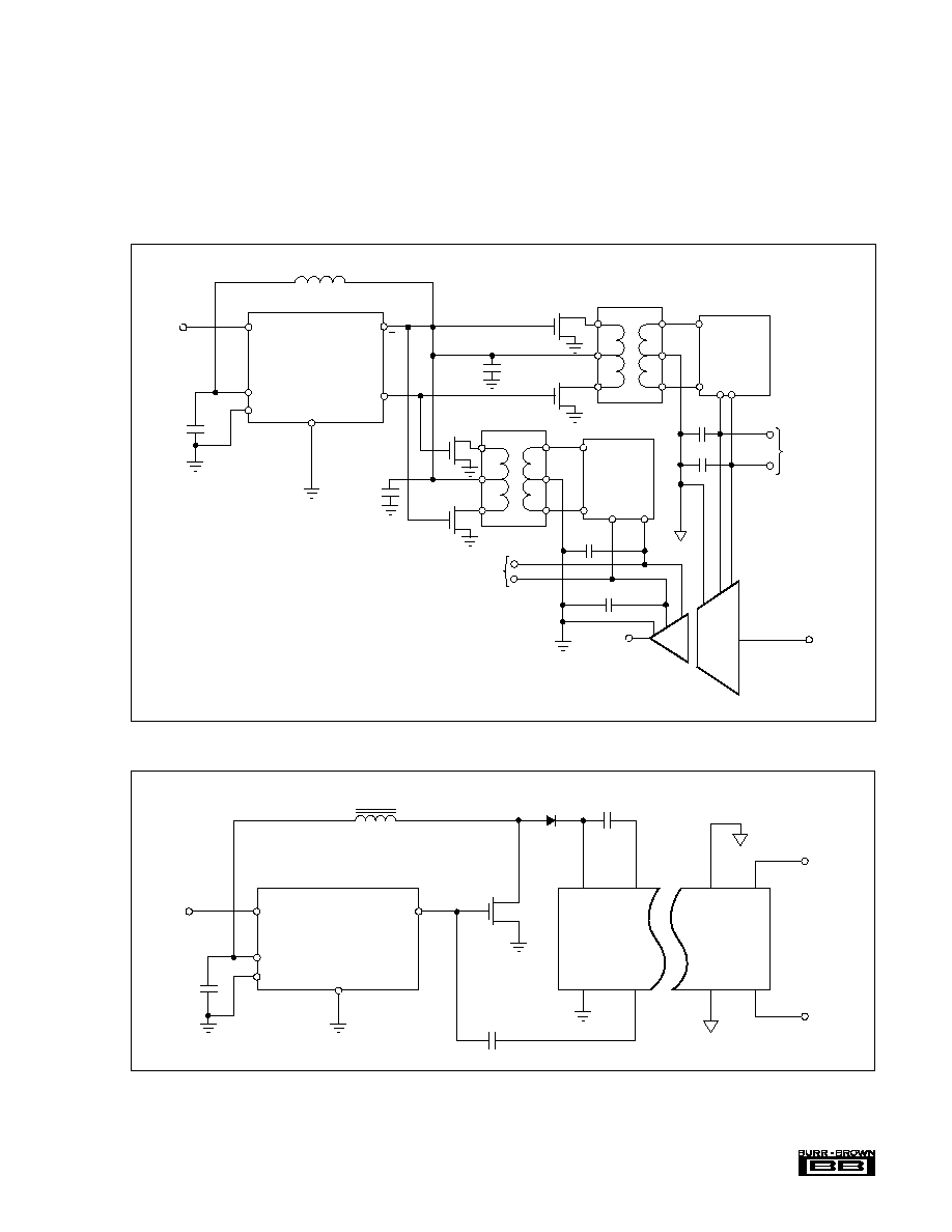
FIGURE 3. Four-Channels of
±
10V Signal Isolation with Channel-to-Channel Isolation.
Æ
PWS750
9
V ±10V
IN
15
1
2
16
Power for
input signal
conditioning
circuitry
0.3µF
0.3µF
4
1
6
8
10
9
V
±10V
OUT
0.3µF
Power for
output
circuitry
0.3µF
1
4
ISO122P
7
D
PWS750-3U
S
5
6
7
4
D
S
3
2
TNO604
10µH
PWS750-1U
+V
IN
V
D
7
3
11
Input
Gnd
14
16
T
0.3µF
0.3µF
D
PWS750-3U
S
5
6
7
4
D
S
3
2
PWS750-4U
3
6
3
5V
TNO604
TN0604
TN0604
PWS750-4U
1
T
180mA
3 Turns
PWS750-1U
7
3
11
14
1
TNO604
D
S
G
47pF
Gnd
0.3µF
+5V
1µF
16
19
15
14
PWS726
4
1
30
32
≠V
O
+V
O
V
D
TTL In
≠
T
H7F
TO7-14-3.5
The minimum AC barrier voltage that initiates partial dis-
charge above 5pC is defined as the "inception voltage."
Decreasing the barrier voltage to a lower level is required
before partial discharge ceases; this is known as "extinction
voltage." We have developed a package insulation system to
yield an inception voltage greater than 1200Vrms so that
transient voltages below this level will not damage the
isolation barrier. The extinction voltage is above 750Vrms
so that even overvoltage-induced partial discharge will cease
once the barrier voltage is reduced to the rated value.
Previous high voltage test methods relied on applying a
large enough overvoltage (above rating) to break down
marginal units, but not so high as to permanently damage
good ones. Our partial discharge testing gives us more
confidence in barrier reliability than breakdown/no break-
down criteria.
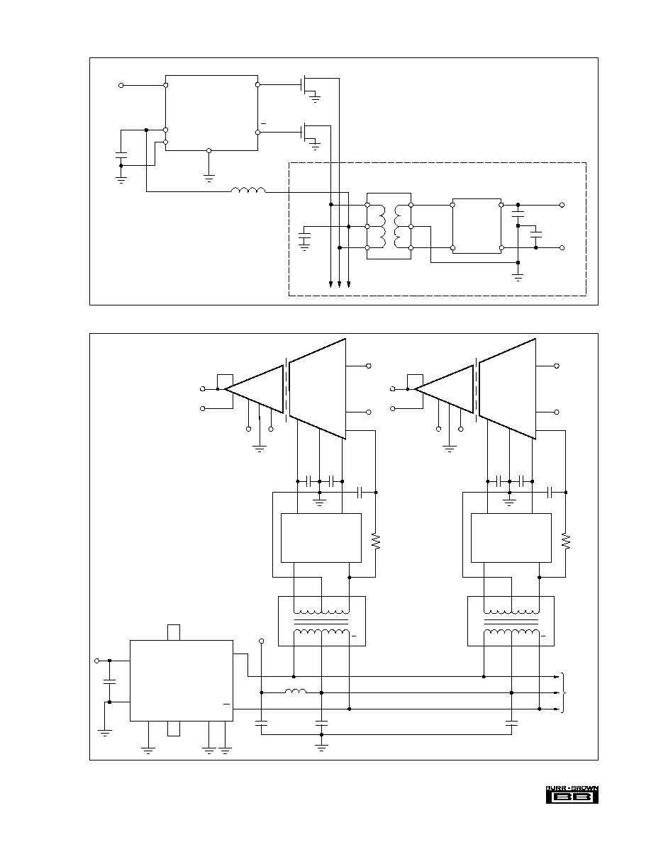
FIGURE 5. A PWS750 Driver Can Be Used to Boost the Input Voltage to 15V to Power a PWS726 From a 5V Supply.
FIGURE 4. A Complete
±
10V Signal Acquisition System Operating From a Single 5V Supply.

10
Æ
PWS750
1
4
D
S
10µH
PWS750-1U
+V
IN
V
D
7
Input
Gnd
14
1
T
0.3µF
PWS750-3U
4
5
3
2
1
PWS740-2
0.3µF
6
3
G
6
2N7008
0.3µF
Output
Gnd
+V
O
O
≠V
D
S
16
G
2N7008
3
11
V ±10V
IN
≠V +V
Power for input signal
conditioning circuits
1
4
2
3
22
24
21
ISO103
12
16
14
10
V ±10V
OUT
0.3µF
1
4
D
S
5
6
7
2
D
S
4
3
TN0604
10µH
PWS750-1U
+V
IN
V
D
7
3
11
Input
Gnd
14
16
1
0.3µF
0.3µF
PWS750-3U
S
D
S
PWS750-4U
0.3µF
6
3
5V
TN0604
TN0604
TN0604
PWS750-4U
D
G
G
G
G
1
4
PWS750-3U
6
3
0.3µF
+V
O
≠V
O
11
6
7
2
4
3
5
FIGURE 6. Powering the Internally Powered ISO103 Isolation Buffer From a Single 5V Supply. Two Power Channels Are
Necessary to Provide the 80mA Nominal for the +V of the ISO103.
FIGURE 7. 1500VAC Isolation Using PWS740-2 Transformer.
Æ
PWS750
11
TTL
6, 7
8
12
13
IN
4
5
T
T
PWS740-3
PWS750-3
0.3µF
V
IN
20µH
PWS745-1
5V
11
16
1
2, 3
14, 15
V
IN1
AC
GND
AC
3
6
PWS745-2
PWS740-2
PWS750-2
Gnd1
1
4
20k
20pF
+V
S1
≠V
S1
ISO120
23
21
V+
V≠
15
12
16
11
10
V
OUT1
9
22
Ext
Osc
4
24
3
0.3µF
PWS740-3
PWS750-3
V
IN2
AC
GND
AC
3
6
PWS745-2
PWS740-2
PWS750-2
Gnd2
1
4
20k
20pF
+V
S2
T
O
ISO120
23
21
22
Ext
Osc
4
24
3
0.3µF
10µF
V+
Up to 6
more
channels
V+
V≠
15
12
16
11
10
V
OUT2
9
V
D
T
O
T
O
V
D
T
O
0.3µF 0.3µF
0.3µF 0.3µF
V≠
V+
AC
AC
V≠
V+
AC
AC
1
4
D
S
D
S
10µH
PWS750-1U
+V
IN
V
D
7
3
11
Input
Gnd
14
T
1
T
16
0.3µF
PWS750-3U
5
6
4
3
2
PWS750-2U
0.3µF
6
3
G
G
7
2N7010
0.3µF
Output
Gnd
+V
O
O
≠V
Duplicate for up to 8 Channels
2N7010
FIGURE 8. FET Pair Driving Up to Eight-Channels.
FIGURE 9. Synchronized-Multichannel Isolation System.