 | ÐлекÑÑоннÑй компоненÑ: XTR103BP | СкаÑаÑÑ:  PDF PDF  ZIP ZIP |
Äîêóìåíòàöèÿ è îïèñàíèÿ www.docs.chipfind.ru
©
1992 Burr-Brown Corporation
PDS-1145E
Printed in U.S.A. October, 1993
International Airport Industrial Park · Mailing Address: PO Box 11400, Tucson, AZ 85734 · Street Address: 6730 S. Tucson Blvd., Tucson, AZ 85706 · Tel: (520) 746-1111 · Twx: 910-952-1111
Internet: http://www.burr-brown.com/ · FAXLine: (800) 548-6133 (US/Canada Only) · Cable: BBRCORP · Telex: 066-6491 · FAX: (520) 889-1510 · Immediate Product Info: (800) 548-6132
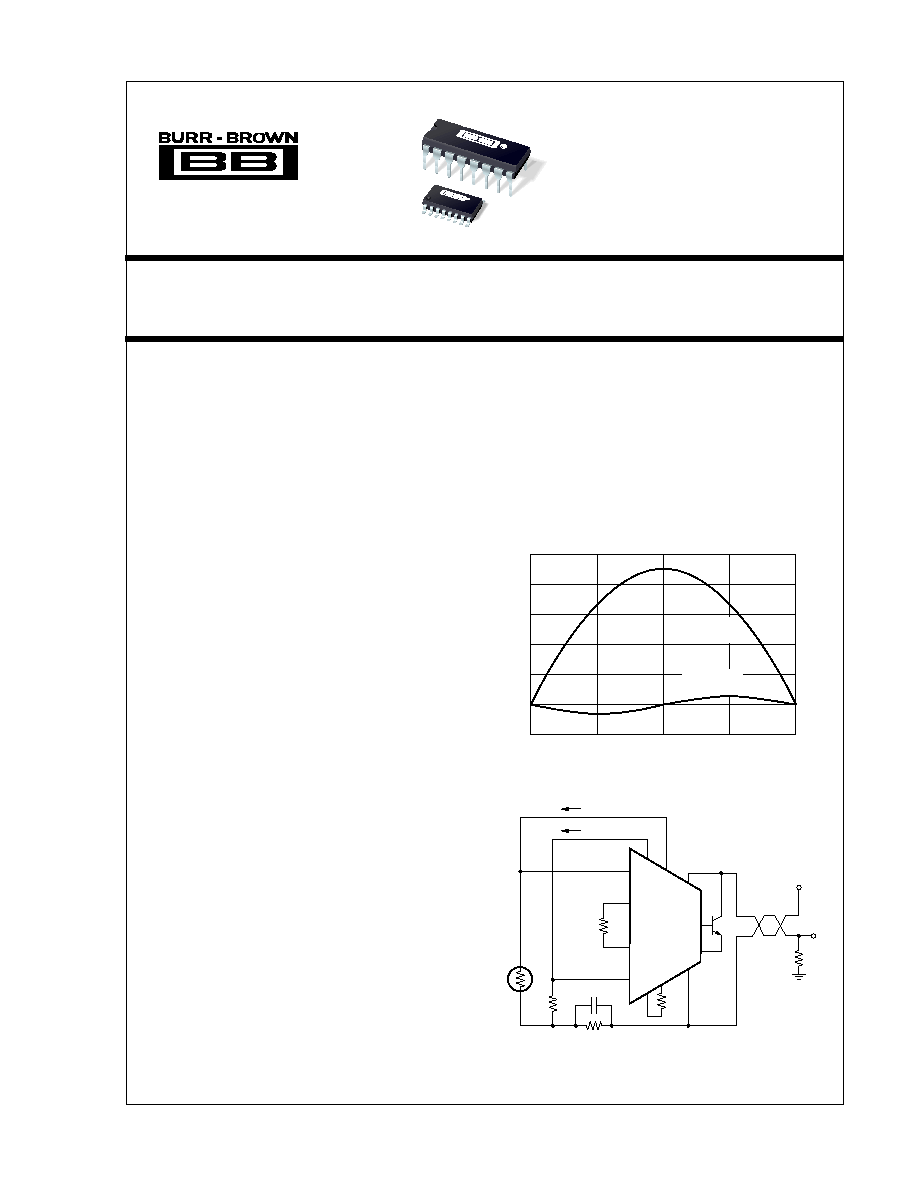
200°C
Pt100 NONLINEARITY CORRECTION
USING XTR103
Process Temperature (°C)
+850°C
5
4
3
2
1
0
1
Uncorrected
RTD Nonlinearity
Corrected
Nonlinearity
Nonlinearity (%)
XTR103
4-20mA Current Transmitter with
RTD EXCITATION AND LINEARIZATION
FEATURES
q
LESS THAN
±
1% TOTAL ADJUSTED
ERROR, 40
°
C TO +85
°
C
q
RTD EXCITATION AND LINEARIZATION
q
TWO OR THREE-WIRE RTD OPERATION
q
WIDE SUPPLY RANGE: 9V to 40V
q
HIGH PSR: 110dB min
q
HIGH CMR: 80dB min
APPLICATIONS
q
INDUSTRIAL PROCESS CONTROL
q
FACTORY AUTOMATION
q
SCADA
DESCRIPTION
The XTR103 is a monolithic 4-20mA, two-wire
current transmitter designed for Platinum RTD tem-
perature sensors. It provides complete RTD current
excitation, instrumentation amplifier, linearization, and
current output circuitry on a single integrated circuit.
Versatile linearization circuitry provides a 2nd-order
correction to the RTD, typically achieving a 40:1
improvement in linearity.
Instrumentation amplifier gain can be configured for a
wide range of temperature measurements. Total
adjusted error of the complete current transmitter,
including the linearized RTD is less than
±
1% over the
full 40 to +85
°
C operating temperature range. This
includes zero drift, span drift and nonlinearity. The
XTR103 operates on loop power supply voltages down
to 9V.
The XTR103 is available in 16-pin plastic DIP and
SOL-16 surface-mount packages specified for the
40
°
C to +85
°
C temperature range.
RTD
XTR103
R
L
4-20 mA
V
PS
+
9 to 40V
I
R
= 0.8mA
I
R
= 0.8mA
V
O
R
LIN
R
G
®
XTR103
XTR103

2
®
XTR103
T
Specification same as XTR103BP.
NOTES: (1) Includes corrected Pt100 nonlinearity for process measurement spans greater than 100
°
C, and over-temperature zero and span effects. Does not include
initial offset and gain errors which are normally trimmed to zero at 25
°
C. (2) Describes accuracy of the 4mA low-scale offset current. Does not include input amplifier
effects. Can be trimmed to zero. (3) Voltage measured with respect to I
O
pin. (4) Does not include TCR of gain-setting resistor, R
G
. (5) Measured with R
LIN
=
to
disable linearization feature.
I
O
= V
IN
· (0.016 + 40/R
G
) + 4mA, V
IN
in Volts, R
G
in
SPECIFICATIONS
ELECTRICAL
At T
A
= +25
°
C, V+
= 24V, and 2N6121 external transistor, unless otherwise noted.
XTR103BP/BU
XTR103AP/AU
PARAMETER
CONDITIONS
MIN
TYP
MAX
MIN
TYP
MAX
UNITS
OUTPUT
Output Current Equation
A
Total Adjusted Error
(1)
T
MIN
to T
MAX
±
1
±
2
% of FS
Output Current, Specified Range
4
20
T
T
mA
Over-Scale Limit
34
40
T
T
mA
Under Scale-Limit
3.6
3.8
T
T
mA
Full Scale Output Error
V
IN
= 1V, R
G
=
±
15
±
50
T
±
100
µ
A
Noise: 0.1Hz to 1kHz
R
G
= 40
8
T
µ
Ap-p
ZERO OUTPUT
(2)
V
IN
= 0, R
G
=
4
T
mA
Initial Error
±
5
±
50
T
±
100
µ
A
vs Temperature
±
0.2
±
0.5
T
±
1
µ
A/
°
C
vs Supply Voltage, V+
V+ = 9V to 40V
(3)
0.5
2
T
T
µ
A/V
vs Common-Mode Voltage
V
CM
= 2V to 4V
(3)
0.1
2
T
T
µ
A/V
SPAN
Span Equation (Transconductance)
S = 0.016 + 40/R
G
T
A/V
Untrimmed Error
R
G
75
±
0.1
±
1
T
T
%
vs Temperature
(4)
±
20
±
50
T
±
100
ppm/
°
C
Nonlinearity: Ideal Input
0.01
T
%
RTD Input
Pt100: 200
°
C to +850
°
C
0.1
T
%
R
LIN
= 1127
INPUT
Differential Range
R
G
=
1
T
V
Input Voltage Range
(3)
2
4
T
T
V
Common-Mode Rejection
V
IN
= 2V to 4V
(3)
80
100
T
T
dB
Impedance: Differential
3
T
G
Common-Mode
0.5
T
G
Offset Voltage
±
0.5
±
2.5
T
T
mV
vs Temperature
±
1
±
2.5
±
2
±
5
µ
V/
°
C
vs Supply Voltage, V+
V+ = 9V to 40V
(3)
110
130
T
T
dB
Input Bias Current
100
250
T
T
nA
vs Temperature
0.1
2
T
T
nA/
°
C
Input Offset Current
2
20
T
T
nA
vs Temperature
0.01
0.25
T
T
nA/
°
C
CURRENT SOURCES
(5)
Current
0.8
T
mA
Accuracy
±
0.25
±
0.5
T
±
1
%
vs Temperature
±
25
±
50
±
50
±
100
ppm/
°
C
vs Power Supply, V+
V+ = 9V to 40V
(3)
50
T
ppm/V
Compliance Voltage
(3)
(V
IN
) 0.2
(V+) 5
T
T
V
Matching
±
0.5
T
%
vs Temperature
±
10
±
25
T
±
50
ppm/
°
C
vs Power Supply, V+
V+ = 9V to 40V
(3)
10
T
ppm/V
POWER SUPPLY
Voltage Range
(3)
, V+
9
40
T
T
V
TEMPERATURE RANGE
Specification, T
MIN
to T
MAX
40
85
T
T
°
C
Operating
40
125
T
T
°
C
JA
80
T
°
C/W
XTR103
3
®
PIN CONFIGURATION
Power Supply, V+ (referenced to I
O
pin) .......................................... 40V
Input Voltage, V
+
IN
, V
IN
(referenced to I
O
pin) ........................ 0V to V+
Storage Temperature Range ........................................ 55
°
C to +125
°
C
Lead Temperature (soldering, 10s) .............................................. +300
°
C
Output Current Limit ............................................................... Continuous
Junction Temperature ................................................................... +165
°
C
ABSOLUTE MAXIMUM RATINGS
Zero Adjust
Zero Adjust
V
IN
V
IN
R
G
R
G
I
O
R
LIN
Zero Adjust
B (Base)
E
INT
(Internal Emitter)
I
R2
I
R1
E (Emitter)
V+
R
LIN
1
2
3
4
5
6
7
8
16
15
14
13
12
11
10
9
+
ELECTROSTATIC
DISCHARGE SENSITIVITY
This integrated circuit can be damaged by ESD. Burr-Brown
recommends that all integrated circuits be handled with
appropriate precautions. Failure to observe proper handling
and installation procedures can cause damage.
ESD damage can range from subtle performance degradation
to complete device failure. Precision integrated circuits may
be more susceptible to damage because very small parametric
changes could cause the device not to meet its published
specifications.
TOP VIEW
The information provided herein is believed to be reliable; however, BURR-BROWN assumes no responsibility for inaccuracies or omissions. BURR-BROWN assumes
no responsibility for the use of this information, and all use of such information shall be entirely at the user's own risk. Prices and specifications are subject to change
without notice. No patent rights or licenses to any of the circuits described herein are implied or granted to any third party. BURR-BROWN does not authorize or warrant
any BURR-BROWN product for use in life support devices and/or systems.
PACKAGE
DRAWING
TEMPERATURE
PRODUCT
PACKAGE
NUMBER
(1)
RANGE
XTR103AP
16-pin Plastic DIP
180
40
°
C to +85
°
C
XTR103BP
16-pin Plastic DIP
180
40
°
C to +85
°
C
XTR103AU
SOL-16 Surface Mount
211
40
°
C to +85
°
C
XTR103BU
SOL-16 Surface Mount
211
40
°
C to +85
°
C
NOTE: (1) For detailed drawing and dimension table, please see end of data
sheet, or Appendix C of Burr-Brown IC Data Book.
PACKAGE/ORDERING INFORMATION
4
®
XTR103
100
1k
10k
100k
0
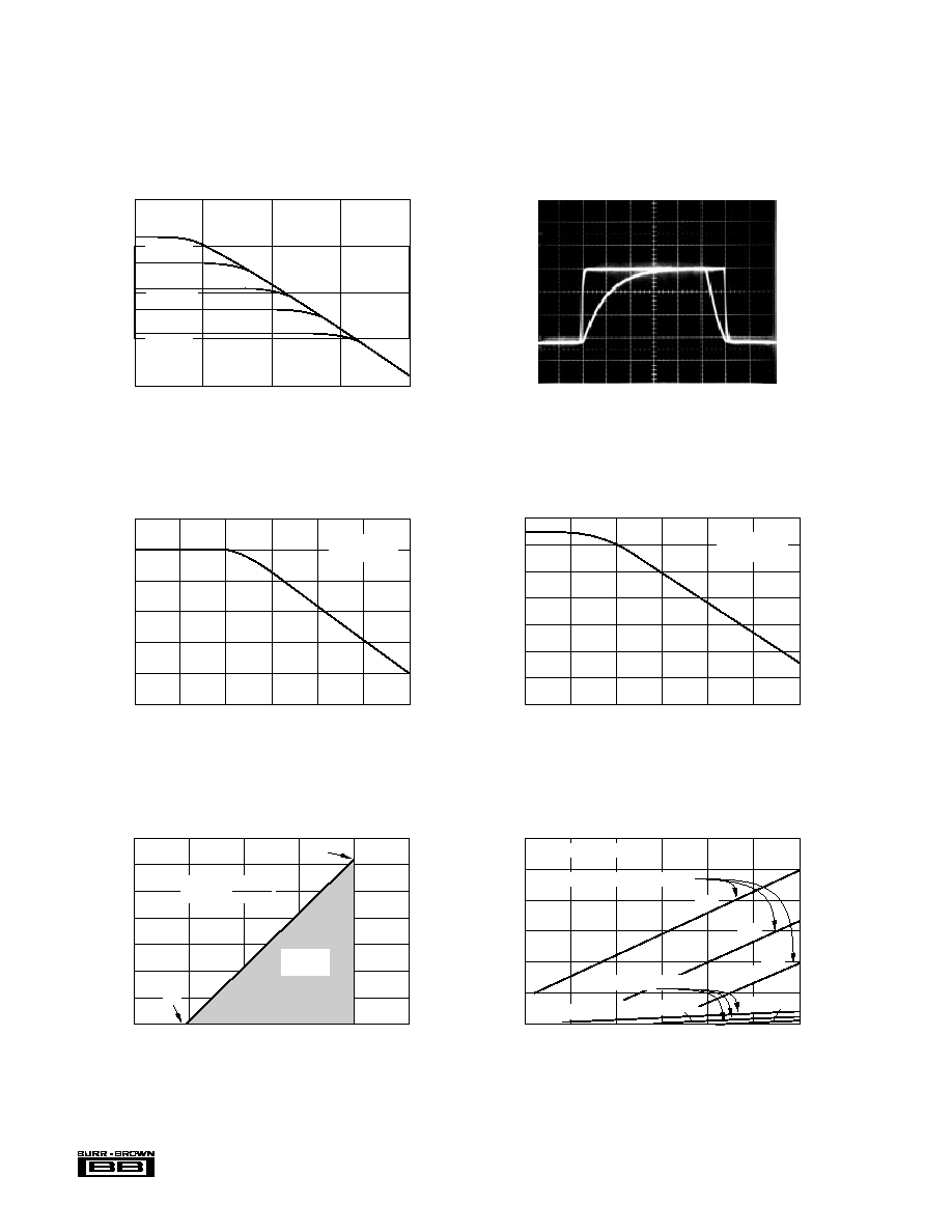
Frequency (Hz)
TRANSCONDUCTANCE vs FREQUENCY
1M
80
60
40
20
Transconductance (20 Log mA/V)
R
G
= 25
R
G
= 100
R
G
= 400
R
G
= 2k
R
G
=
20mA
4mA
R
S
=
R
S
= 25
STEP RESPONSE
5mA/Div
100
µ
s/Div
0
0.1
1
10
100
1k
10k
Frequency (Hz)
CMR (dB)
COMMON-MODE REJECTION
vs FREQUENCY (RTI)
100k
120
100
80
60
40
20
G = 0.16A/V
(R
G
= 400
)
120
100
80
60
40
20
0.1
0
Frequency (Hz)
Power Supply Rejection (dB)
POWER SUPPLY
REJECTION vs FREQUENCY (RTI)
140
1
10
100
1k
10k
100k
G = 0.16A/V
(R
G
= 400
)
1500
1250
1000
750
500
250
0
10
20
30
40
50
0
Loop Power Supply Voltage, V
PS
(V)
Loop Resistance, R
L
(
)
1550
LOOP RESISTANCE vs LOOP POWER SUPPLY
R
L
max =
(V+) 9V
20mA
1750
Operating
Region
9V
Loop Power Supply Voltage, V
PS
(V)
V (µV)
OS
60
50
40
30
20
10
0
10
20
30
40
R
L
= 100
R
L
= 600
R
L
= 1k
R
L
= 100
R
L
= 600
R
L
= 1k
Without external transistor
Span =
I
O
= 16mA
With external transistor
INPUT OFFSET VOLTAGE vs LOOP POWER SUPPLY
TYPICAL PERFORMANCE CURVES
At T
A
= +25
°
C, V+ = 24VDC, unless otherwise noted.
XTR103
5
®
TYPICAL PERFORMANCE CURVES
(CONT)
At T
A
= +25
°
C, +V
= 24VDC, unless otherwise noted.
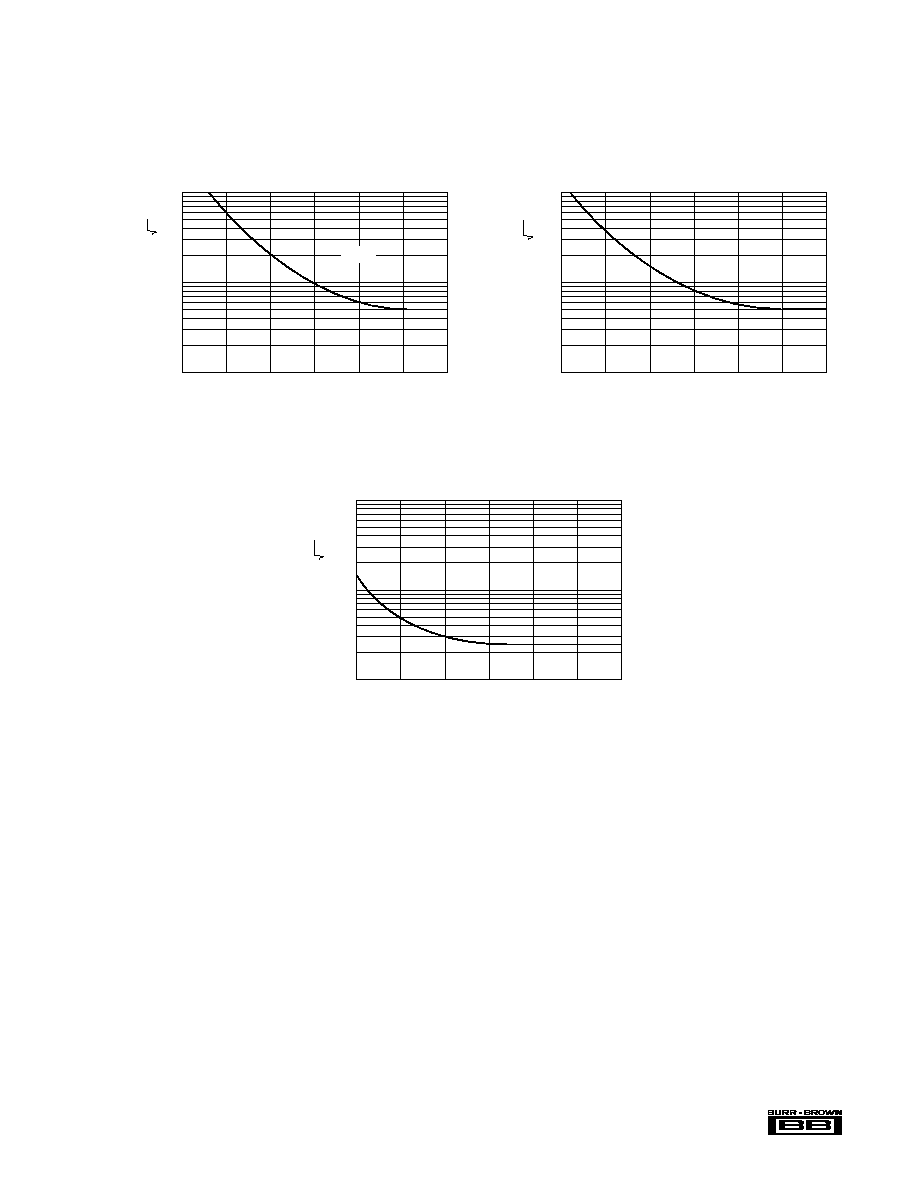
Output Current Noise (pA/ Hz)
0.1
1
100
1k
100k
Frequency (Hz)
OUTPUT CURRENT NOISE DENSITY vs FREQUENCY
10
10
1
0.1
10k
R
G
=
Input Current Noise (pA/ Hz
)
0.1
1
100
1k
100k
Frequency (Hz)
INPUT CURRENT NOISE DENSITY vs FREQUENCY
10
10
1
0.1
10k
0.1
1
100
1k
100k
Frequency (Hz)
INPUT VOLTAGE NOISE DENSITY vs FREQUENCY
Noise Voltage (nV/ Hz
)
10
1k
100
10
10k
6
®
XTR103
+
12
13
4
5
6
3
R
G
XTR103
R = 1.5k
CM
7
I
R
=
0.8mA
0.01µF
I = 4mA + V
IN
(0.016 + )
O
40
R
G
R
Z
RTD
9
8
R
LIN
(2, 3)
NOTES: (1) R
Z
= RTD resistance at the minimum measured temperature.
I
R
=
0.8mA
V
IN
R
G
R
G
V
IN
V
+
IN
I
R
I
R
V+
R
LIN
R
LIN
I
O
E
B
(1, 3)
R
G
=
2500
1
(2)
1
V
FS
V
PS
+
11
4-20 mA
0.01µF
+
15
10
V
IN
= V
+
IN
V
IN
= I
R
(RTD R
Z
)
R
L
(3)
Q
1
, where V
FS
is Full Scale V
IN
.
(3) See Table I for values.
TYPE
2N4922
TIP29B
TIP31B
PACKAGE
TO-225
TO-220
TO-220
Possible choices for Q
1
(see text).
APPLICATION INFORMATION
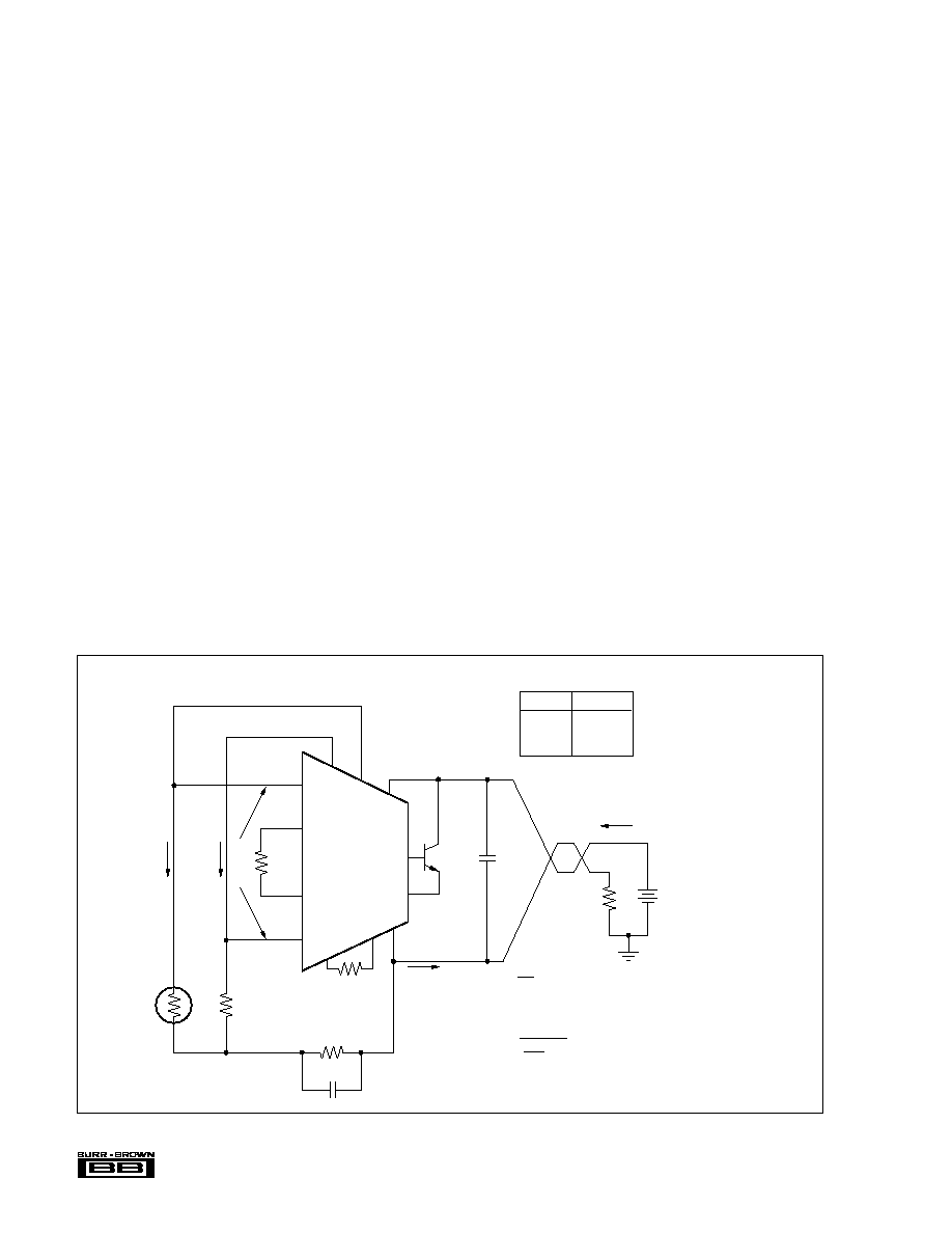
Figure 1 shows the basic connection diagram for the XTR103.
The loop power supply, V
PS
provides power for all circuitry.
Output loop current is measured as a voltage across the
series load resistor, R
L
.
Two matched 0.8mA current sources drive the RTD and
zero-setting resistor, R
Z
. The instrumentation amplifier in-
put of the XTR103 measures the voltage difference between
the RTD and R
Z
. The value of R
Z
is chosen to be equal to
the resistance of the RTD at the low-scale (minimum)
measurement temperature. R
Z
can be adjusted to achieve
4mA output at the minimum measurement temperature to
correct for input offset voltage and reference current mis-
match of the XTR103.
R
CM
provides an additional voltage drop to bias the inputs of
the XTR103 within their common-mode range. Resistor, R
G
,
sets the gain of the instrumentation amplifier according to
the desired temperature measurement range.
The transfer function through the complete instrumentation
amplifier and voltage-to-current converter is:
I
O
= V
IN
· (0.016 + 40/R
G
) + 4mA,
(V
IN
in volts, R
G
in ohms, R
LIN
=
)
where V
IN
is the differential input voltage. With no R
G
connected (R
G
=
), a 0V to 1V input produces a 4-20mA
output current. With R
G
= 25
, a 0V to 10mV input pro-
duces a 4-20mA output current. Other values for R
G
can be
calculated according to the desired full-scale input voltage,
V
FS
, with the formula in Figure 1.
Negative input voltage, V
IN
, will cause the output current to
be less than 4mA. Increasingly negative V
IN
will cause the
output current to limit at approximately 3.6mA.
Increasingly positive input voltage (greater than V
FS
) will
produce increasing output current according to the transfer
function, up to the output current limit of approximately
34mA.
EXTERNAL TRANSISTOR
Transistor Q
1
conducts the majority of the signal-dependent
4-20mA loop current. Using an external transistor isolates
the majority of the power dissipation from the precision
input and reference circuitry of the XTR103, maintaining
excellent accuracy.
Since the external transistor is inside a feedback loop its
characteristics are not critical. Requirements are: V
CEO
=
45V min,
= 40 min and P
D
= 800mW. Power dissipation
requirements may be lower if the loop power supply voltage
is less than 40V. Some possible choices for Q
1
are listed in
Figure 1.
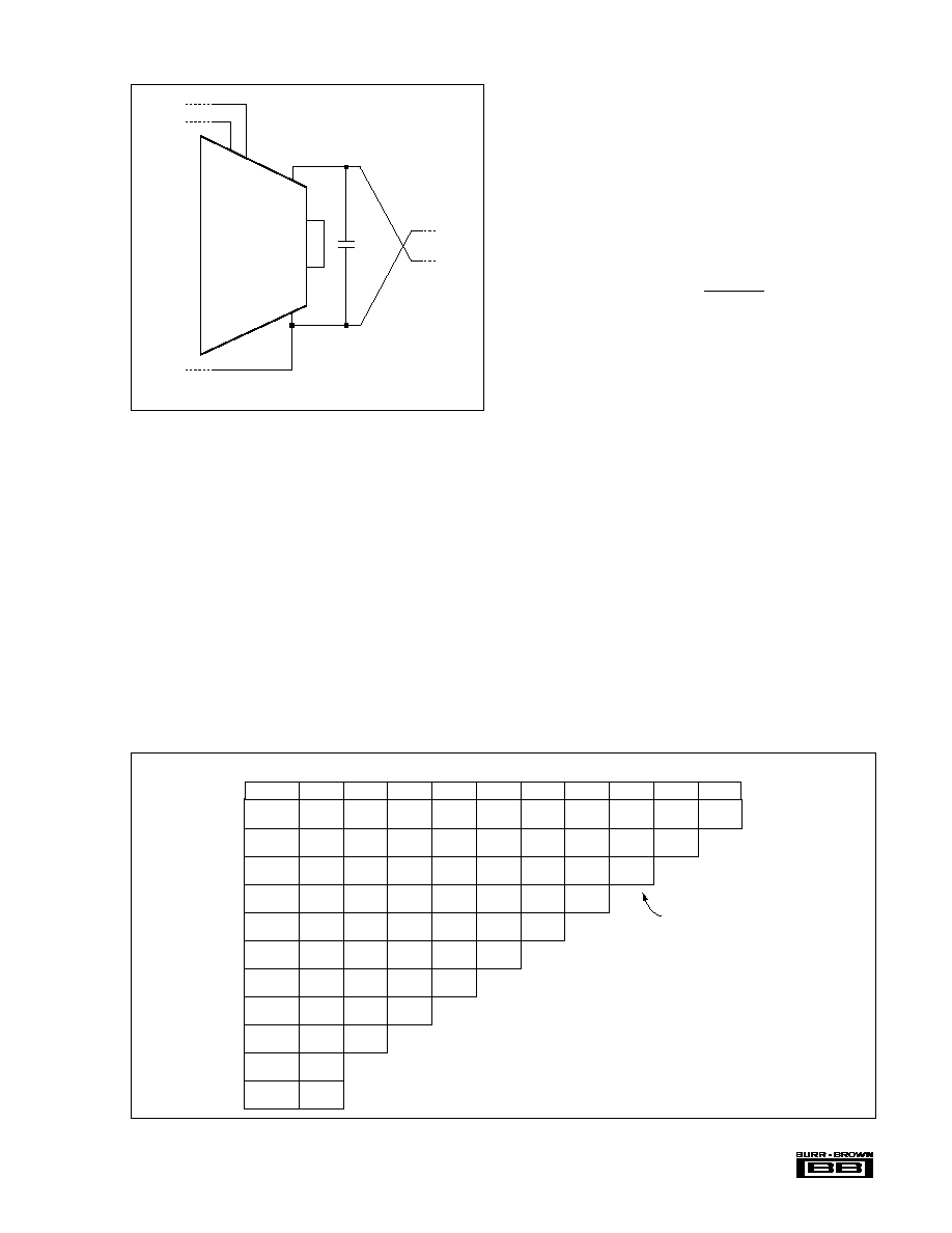
The XTR103 can be operated without this external transistor
by connecting pin 11 to 14 (see Figure 2). Accuracy will be
somewhat degraded by the additional internal power dissipa-
tion. This effect is most pronounced when the input stage is
set for high gain (for low full-scale input voltage). The
typical performance curve "Input Offset Voltage vs Loop
Supply Voltage" describes this behavior.
FIGURE 1. Basic RTD Temperature Measurement Circuit.
XTR103
7
®
FIGURE 2. Operation Without External Transistor.
TABLE I. R
Z
, R
G
, and R
LIN
Resistor Values for Pt100 RTD.
T
MIN
100
°
C
200
°
C
300
°
C
400
°
C
500
°
C
600
°
C
700
°
C
800
°
C
900
°
C
1000
°
C
200
°
C
18/90
18/185
18/286
18/396
18/515
18/645
18/788
18/946
18/1120 18/1317
653
838
996
1087
1131
1152
1159
1158
1154
1140
100
°
C
60/84
60/173
60/270
60/374
60/487
60/610
60/746
60/895
60/1061
1105
1229
1251
1249
1231
1207
1181
1155
1128
0
°
C
100/81
100/167 100/260 100/361 100/469 100/588 100/718 100/860
1287
1258
1229
1201
1173
1145
1117
1089
100
°
C
138/78
138/162 138/252 138/349 138/453 138/567 138/691
1211
1183
1155
1127
1100
1073
1046
200
°
C
175/76
175/157 175/244 175/337 175/437 175/546
1137
1110
1083
1056
1030
1003
300
°
C
212/73
212/152 212/235 212/325 212/422
1066
1039
1013
987
962
400
°
C
247/71
247/146 247/227 247/313
996
971
946
921
500
°
C
280/68
280/141 280/219
930
905
881
600
°
C
313/66
313/136
865
841
700
°
C
345/64
803
800
°
C
375/61
743
MEASUREMENT TEMPERATURE SPAN
T (
°
C)
R
Z
/R
G
R
LIN
11
14
XTR103
0.01µF
E
E
INT
I
O
V+
For operation without external
transistor, connect pin 11 to
pin 14. See text for discussion
of performance.
10
7
(Values are in
.)
NOTE: Values shown are for a Pt100 RTD.
Double (x2) all values for Pt200.
LOOP POWER SUPPLY
The voltage applied to the XTR103, V+, is measured with
respect to the I
O
connection, pin 7. V+ can range from 9V
to
40V. The loop supply voltage, V
PS
, will differ from the
voltage applied to the XTR103 according to the voltage drop
on the current sensing resistor, R
L
(plus any other voltage
drop in the line).
If a low loop supply voltage is used, R
L
must be made a
relatively low value to assure that V+ remains 9V or greater
for the maximum loop current of 20mA. It may, in fact, be
prudent to design for V+ equal or greater than 9V with loop
currents up to 34mA to allow for out-of-range input condi-
tions. The typical performance curve "Loop Resistance vs
Loop Power Supply" shows the allowable sense resistor
values for full-scale 20mA.
The low operating voltage (9V) of the XTR103 allows
operation directly from personal computer power supplies
(12V
±
5%). When used with the RCV420 Current Loop
Receiver
(Figure 8), load resistor voltage drop is limited to
1.5V.
LINEARIZATION
On-chip linearization circuitry creates a signal-dependent
variation in the two matching current sources. Both current
sources are varied equally according to the following equa-
tion:
I
R1
= I
R2
= 0.8 +
(I
R
in mA, V
IN
in volts, R
LIN
in ohms)
(maximum I
R
= 1.0mA)
This varying excitation provides a 2nd-order term to the
transfer function (including the RTD) which can correct the
RTD's nonlinearity. The correction is controlled by resistor
R
LIN
which is chosen according to the desired temperature
measurement range. Table I provides the R
G
, R
Z
and R
LIN
resistor values for a Pt100 RTD.
If no linearity correction is desired, do not connect a resistor
to the R
LIN
pins (R
LIN
=
). This will cause the excitation
current sources to remain a constant 0.8mA.
ADJUSTING INITIAL ERRORS
Most applications will require adjustment of initial errors.
Offset errors can be corrected by adjustment of the zero
resistor, R
Z
.
Figure 3 shows another way to adjust zero errors using the
output current adjustment pins of the XTR103. This provides
a minimum of
±
300
µ
A (typically
±
500
µ
A) adjustment around
the initial low-scale output current. This is an output current
adjustment which is independent of the input stage gain set
R
LIN
500 · V
IN
8
®
XTR103
2
16
XTR103
1
10k
XTR103
5k
5k
1
(a)
(b)
2
16
±500µA typical
output current
adjustment range.
±50µA typical
output current
adjustment range.
FIGURE 3. Low-Scale Output Current Adjustment.
with R
G
. If the input stage is set for high gain (as required
with narrow temperature measurement spans) the output
current adjustment may not provide sufficient range. In these
cases, offset can be nulled by adjusting the value of R
Z
.
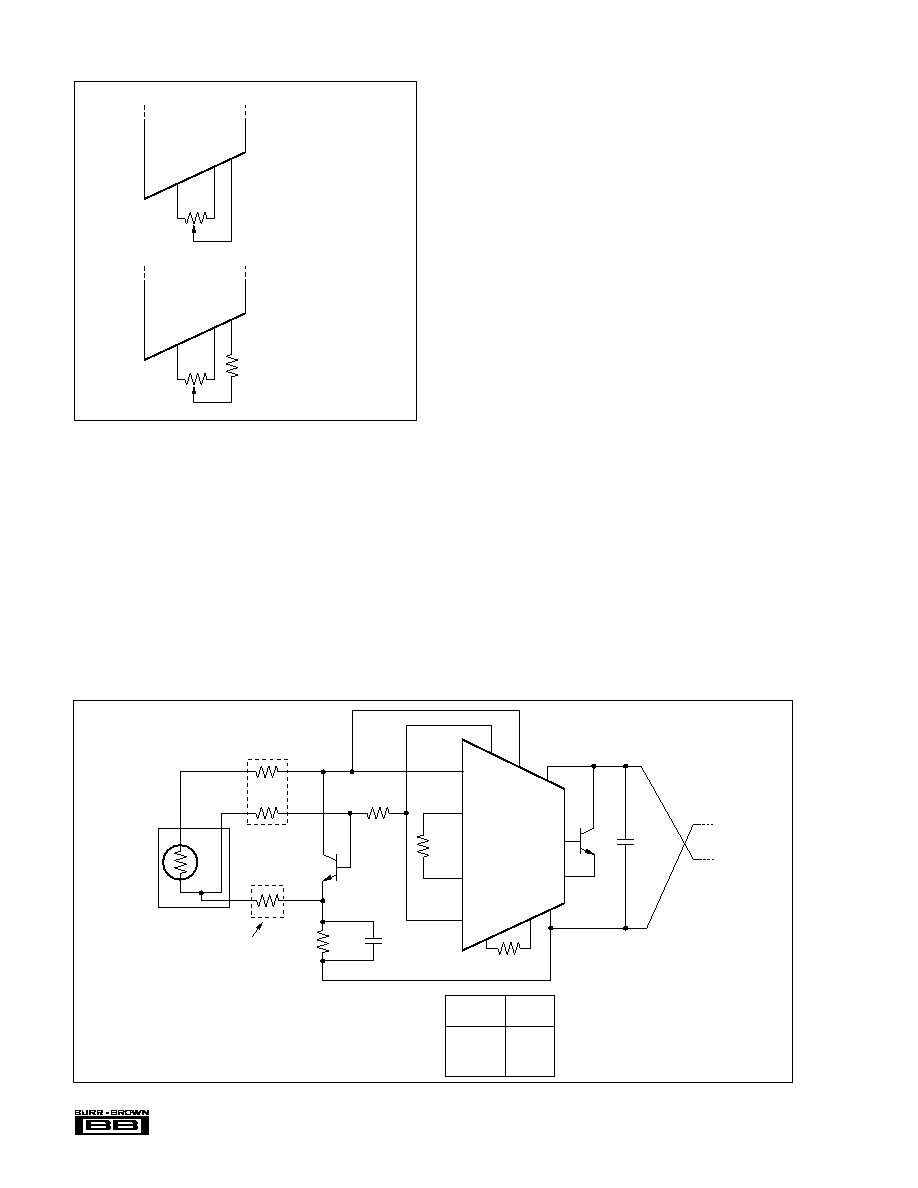
TWO-WIRE AND
THREE-WIRE RTD CONNECTIONS
In Figure 1, the RTD can be located remotely simply by
extending the two connections to the RTD. With this two-
wire connection to the RTD, line resistance will introduce
error. This error can be partially corrected by adjusting the
values of R
Z
,
R
G
, and R
LIN
.
Figure 4, shows a three-wire RTD connection for improved
accuracy with remotely located RTDs. R
Z
's current is routed
through a third wire to the RTD. Assuming line resistance is
equal in RTD lines 1 and 2, this produces a small common-
mode voltage which is rejected by the XTR103.
OPEN-CIRCUIT DETECTION
The optional transistor Q
2
in Figure 4 provides predictable
behavior with open-circuit RTD connections. It assures that
if any one of the three RTD connections is broken, the
XTR103's output current will go to either its high current
limit (
34mA) or low current limit (
3.6mA). This is easily
detected as an out-of-range condition.
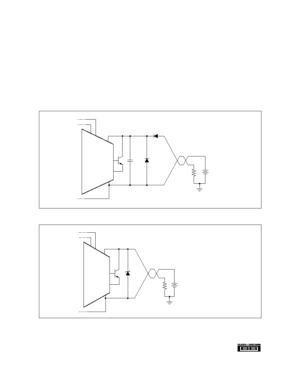
REVERSE-VOLTAGE PROTECTION
Figure 5 shows two ways to protect against reversed output
connection lines. Trade-offs in an application will determine
which technique is better. D
1
offers series protection, but
causes a 0.7V loss in loop supply voltage. This may be
undesirable if V+ can approach the 9V limit. Using D
2
(without D
1
) has no voltage loss, but high current will flow
in the loop supply if the leads are reversed. This could
damage the power supply or the sense resistor, R
L
. A diode
with a higher current rating is needed for D
2
to withstand the
highest current that could occur with reversed lines.
SURGE PROTECTION
Long lines are subject to voltage surges which can damage
semiconductor components. To avoid damage, the maxi-
mum applied voltage rating for the XTR103 is 40V. A zener
diode may be used for D
2
(Figure 6) to clamp the voltage
applied to the XTR103 to a safe level. The loop power
supply voltage must be lower than the voltage rating of the
zener diode.
FIGURE 4. Three-Wire Connection for Remotely Located RTDs.
12
13
4
5
6
3
R
G
XTR103
7
9
8
R
G
R
G
V
IN
V
+
IN
I
R
I
R
V+
10
Q
1
RTD
R
CM
R
LIN
Q
2
*
R
Z
(R
LINE
)
1
2
3
Resistance in this line causes
a small common-mode voltage
which is rejected by XTR103.
line resistances here creates
a small common-mode voltage
which is rejected by XTR103.
*Q
2
optional. Provides
predictable output
current if any one
RTD connection
is broken:
Open RTD
Terminal
I
O
1
2
3
34mA
3.6mA
3.6mA
Equal
15
11
0.01µF
0.01µF
1.5k
2N2222
XTR103
9
®
There are special zener diode types specifically designed to
provide a very low impedance clamp and withstand large
energy surges. These devices normally have a diode charac-
teristic in the forward direction which also protects against
reversed loop connections. As noted earlier, reversed loop
connections would produce a large loop current, possibly
damaging R
L
.
RADIO FREQUENCY INTERFERENCE
The long wire lengths of current loops invite radio frequency
interference. RF can be rectified by the sensitive input
circuitry of the XTR103 causing errors. This generally
appears as an unstable output current that varies with the
position of loop supply or input wiring.
If the RTD sensor is remotely located, the interference may
enter at the input terminals. For integrated transmitter as-
semblies with short connection to the sensor, the interfer-
ence more likely comes from the current loop connections.
Bypass capacitors on the input often reduce or eliminate this
interference. Connect these bypass capacitors to the I
O
terminal as shown in Figure 7. Although the DC voltage at
the I
O
terminal is not equal to 0V (at the loop supply, V
PS
)
this circuit point can be considered the transmitter's "ground."
FIGURE 5. Reverse Voltage Protection.
XTR103
7
V+
I
O
E
B
V
PS
1N4148
D
1
10
0.01µF
R
L
D
2
1N4001
15
11
Use either D
1
or D
2
.
See "Reverse Voltage Protection."
FIGURE 6. Over-Voltage Surge Protection.
XTR103
V+
I
O
E
B
V
PS
(1)
Maximum V
PS
must be less
than minimum voltage rating
of zener diode.
NOTE: (1) Zener diode 36V: 1N4753A
or
General Semiconductor Transorb
TM
1N6286A
Use lower voltage zener diodes with loop
power supply voltages less than 30V for
increased protection.
10
15
11
7
R
L
10
®
XTR103
XTR103
7
0.01µF
5
4
2
3
15
13
14
11
10
12
12
13
8
9
10
R
LIN
R
G
R
Z
5
6
3
4
1.5k
0.01µF
I
O
= 4-20mA
RCV420
16
11
1N4148
RTD
15
E
B
R
G
R
G
V
+
IN
I
R
I
R
V+
I
O
V
IN
16
2
15
10
8
7
9
V
V
O
V+
0 5V
ISO122
1
+15V
0
15V
1µF
1µF
Isolated Power
from PWS740
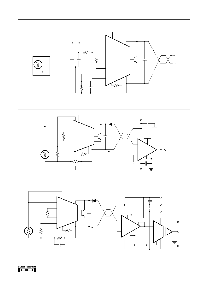
FIGURE 7. Input Bypassing Techniques.
FIGURE 8.
±
12V-Powered Transmitter/Receiver Loop.
FIGURE 9. Isolated Transmitter/Receiver Loop.
12
13
4
5
6
3
R
G
XTR103
7
9
8
R
G
R
G
I
R
I
R
V+
10
RTD
R
CM
R
LIN
R
Z
0.01µF
0.01µF
0.01µF
0.01µF
B
E
15
11
V
+
IN
V
IN
XTR103
7
0.01µF
12V
1µF
5
4
2
3
15
13
14
11
10
12
12
13
8
9
10
R
LIN
R
G
R
Z
138
5
6
3
4
1.5k
0.01µF
I
O
= 4-20mA
1µF
V
O
= 0 to 5V
RCV420
16
+12V
Pt100
11
1N4148
448
100°C to
600°C
1100
15
E
B
R
G
R
G
V
+
IN
I
R
I
R
V+
I
O
V
IN