
FEATURES
D
EASY-TO-DESIGN INPUT/OUTPUT RANGES:
0mA-20mA, 4mA-20mA, 5mA-25mA
AND VOLTAGE OUTPUTS
D
NONLINEARITY: 0.002%
D
LOW OFFSET DRIFT: 1
µ
V/
5
C
D
ACCURACY: 0.015%
D
SINGLE-SUPPLY OPERATION
D
WIDE SUPPLY RANGE: 7V TO 44V
D
OUTPUT ERROR FLAG (EF)
D
OUTPUT DISABLE (OD)
D
ADJUSTABLE VOLTAGE REGULATOR:
3V TO 15V
APPLICATIONS
D
UNIVERSAL VOLTAGE-CONTROLLED
CURRENT SOURCE
D
CURRENT OR VOLTAGE OUTPUT FOR
3-WIRE SENSOR SYSTEMS
D
PLC OUTPUT PROGRAMMABLE DRIVER
D
CURRENT-MODE SENSOR EXCITATION
DESCRIPTION
The XTR111 is a precision voltage-to-current converter
designed for the standard 0mA-20mA or 4mA-20mA
analog signals, and can source up to 36mA. The ratio
between input voltage and output current is set by the
single resistor R
SET
. The circuit can also be modified for
voltage output.
An external P-MOSFET transistor ensures high output
resistance and a broad compliance voltage range
extending from 2V below the supply voltage, V
VSP
, to
voltages well below GND.
The adjustable 3V to 15V sub-regulator output provides
the supply voltage for additional circuitry.
The XTR111 is available in a DFN surface-mount package.
3V
REGF
Regulator
Out
Signal
Input
REGS
24V
I-Mirror
VSP
1
9
8
2
3
G
S
D
VG
IS
Output Disable
Output Failure
0mA to 20mA
4mA to 20mA
OD
EF
VIN
6
4
5
R
SET
I
SET
SET
7
10
GND
I
OUT
= 10
(
)
V
VIN
R
SET
I
OUT
= 10
∑
I
SET
Load
I
OUT
(
±
Load Ground)
XTR111
XTR111
SBOS375 - NOVEMBER 2006
Precision Voltage-to-Current
Converter/Transmitter
XRT11
1
PRODUCTION DATA information is current as of publication date. Products
conform to specifications per the terms of Texas Instruments standard warranty.
Production processing does not necessarily include testing of all parameters.
www.ti.com
Copyright
2006, Texas Instruments Incorporated
Please be aware that an important notice concerning availability, standard warranty, and use in critical applications of Texas Instruments
semiconductor products and disclaimers thereto appears at the end of this data sheet.
All other trademarks are the property of their respective owners.
XTR111
SBOS375 - NOVEMBER 2006
www.ti.com
2
ABSOLUTE MAXIMUM RATINGS
(1)(2)
Power Supply Voltage, V
VSP
+44V
. . . . . . . . . . . . . . . . . . . . . . . . . .
Voltage at SET
(3)
-0.5V to +14V
. . . . . . . . . . . . . . . . . . . . . . . . . . . .
Voltage at IS
(3, 5)
(V
VSP
) - 5.5V to (V
VSP
) + 0.5V
. . . . . . . . . . . . . .
Voltage at REGS, REGF, VIN, OD, EF
-0.5V to (V
VSP
) + 0.5V
. .
Voltage at REGF, VG
-0.5V to (V
VSP
) + 0.5V
. . . . . . . . . . . . . . . . .
Current into any pin
(3, 4)
±
25mA
. . . . . . . . . . . . . . . . . . . . . . . . . . . . .
Output Short-Circuit Duration
(5)
:
VG
Continuous to common and V
VSP
. . . . . . . . . . . . . . . . . . . . .
REGF
Continuous to common and V
VSP
. . . . . . . . . . . . . . . . . . .
Operating Temperature Range
-55
∞
C to +125
∞
C
. . . . . . . . . . . . . . .
Storage Temperature Range
-65
∞
C to +150
∞
C
. . . . . . . . . . . . . . . . .
Electrostatic Discharge Rating (HBM)
2000V
. . . . . . . . . . . . . . . . .
(1) Stresses above these ratings may cause permanent damage.
Exposure to absolute maximum conditions for extended periods
may degrade device reliability. These are stress ratings only, and
functional operation of the device at these or any other conditions
beyond those specified is not supported.
(2) Refer to the Package Option Addendum at the end of this
document for lead temperature ratings.
(3) Input terminals are diode-clamped to the power-supply rails.
Input signals that can swing more than 0.5V beyond the supply
rails must be current limited.
(4) The IS pin can source up to the output current-limit under normal
operating conditions.
(5) See text in Application Section regarding safe voltage ranges
and currents.
This integrated circuit can be damaged by ESD. Texas
Instruments recommends that all integrated circuits be
handled with appropriate precautions. Failure to observe
proper handling and installation procedures can cause damage.
ESD damage can range from subtle performance degradation to
complete device failure. Precision integrated circuits may be more
susceptible to damage because very small parametric changes could
cause the device not to meet its published specifications.
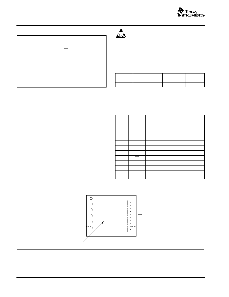
PACKAGE/ORDERING INFORMATION
(1)
PRODUCT
PACKAGE-LEAD
PACKAGE
DESIGNATOR
PACKAGE
MARKING
XTR111
DFN-10
DRC
BSV
(1) For the most current package and ordering information, see the
Package Option Addendum at the end of this document, or see
the TI web site at www.ti.com.
PIN DESCRIPTIONS
PIN
NAME
FUNCTION
1
VSP
Positive Supply
2
IS
Source Connection
3
VG
Gate Drive
4
REGS
Regulator Sense
5
REGF
Regulator Force
6
VIN
Input Voltage
7
SET
Transconductance Set
8
EF
Error Flag (Active Low)
9
OD
Output Disable (Active High)
10
GND
Negative Supply
Pad
Pad
Exposed Thermal Pad must be connected
to GND
PIN CONFIGURATIONS
TOP VIEW
DFN
VSP
IS
VG
REGS
REGF
GND
OD
EF
SET
VIN
1
2
3
4
5
10
9
8
7
6
DFN-10
Pad
Exposed
Thermal
Die Pad
on
Underside.
(Must be
connected
to GND)

XTR111
SBOS375 - NOVEMBER 2006
www.ti.com
3
ELECTRICAL CHARACTERISTICS
Boldface limits apply over the temperature range, T
A
= -40
∞
C to +85
∞
C.
All specifications at T
A
= +25
∞
C,
V
VSP = +24V, R
SET
= 2.0k
; REGF connected to REGS; OD = Low, External FET connected, unless otherwise noted.
XTR111
PARAMETER
CONDITION
MIN
TYP
MAX
UNITS
TRANSMITTER
Transfer Function
I
OUT
= 10
∑
V
VIN/RSET
Specified Output Current
I
OUT
Specified Performance
(1)
0.1
25
mA
Derated Performance
(2)
0 to 36
mA
Current Limit for Output Current
42
±
6
mA
Nonlinearity, IOUT/I
SET
(2, 3)
0.1 to 25mA
0.002
0.02
% of Span
0.1 to 36mA
0.004
% of Span
Offset Current
I
OS
I
OUT
= 4mA
(1)
0.002
0.02
% of Span
vs Temperature
0.0002
0.001
% of Span/
∞
C
vs Supply, V
VSP
8 to 40V Supply
0.0001
0.005
% of Span/V
Span Error, I
OUT
/I
SET
(2)
0.1mA to 25mA
0.015
0.1
% of Span
vs Temperature
(2)
(1)
5
ppm/
∞
C
vs Supply
(1)
0.0001
% of Span/V
Output Resistance
From Drain of Q
EXT
(4)
> 1
G
Output Leakage
OD = high
< 1
µ
A
Input Impedance (VIN)
2.4/30
G
/pF
Input Bias Current (VIN)
I
B
15
25
nA
Input Offset Voltage
(2)
V
OS
V
VIN
= 20mV
0.3
1.5
mV
vs Temperature
1
µ
V/
∞
C
Input Voltage Range
(5)
V
VIN
0 to 12
V
Noise, Referred to Input
(2)
0.1Hz to 10Hz; I
OUT
= 4mA
2.5
µ
V
PP
Dynamic Response
See Dynamic Performance Section
V-Regulator Output (REGF)
Voltage Reference
(2)
R
LOAD
= 5k
2.85
3.0
3.15
V
vs Temperature
(2)
30
ppm/
5
C
vs Supply
(2)
0.1
mV/V
Bias Current into REGS
(2)
0.8
µ
A
Load Regulation
0.6mA to 5mA
3
5
mV/mA
Supply Regulation
(2)
R
LOAD
= 5k
0.01
mV/V
Output Current
5
mA
Short-Circuit Output Current
21
mA
DIGITAL INPUT (OD)
V
IL
Low-Level Threshold
0.6
V
V
IH
High-Level Threshold
1.8
V
Internal Pull-up Current
V
OD
< 5.5V
4
µ
A
DIGITAL OUTPUT (EF)
I
OH
Leakage Current (Open Drain)
1
µ
A
V
OL
Low-Level Output Voltage
I
EF
= 2.2mA
0.8
V
I
OL
Current to 400mV Level
V
EF
= 400mV
2
mA
POWER SUPPLY
Specified Voltage Range
+8
+40
V
Operating Voltage
+7 to +44
V
Quiescent Current
(2)
I
Q
I
OUT
= 0mA
450
550
µ
A
TEMPERATURE RANGE
Specified Range
-40
+85
∞
C
Operating Range
-55
+125
∞
C
Package Thermal Impedance,
q
JA
DFN
70
∞
C/W
(1) Includes input amplifier, but excludes R
SET
tolerance.
(2) See Typical Characteristics.
(3) Span is the change in output current resulting from a full-scale change in input voltage.
(4) Within compliance range limited by (+V
VSP
- 2V) +V
DS
required for linear operation of Q
EXT
.
(5) See Application Information, Input Voltage section.
XTR111
SBOS375 - NOVEMBER 2006
www.ti.com
4
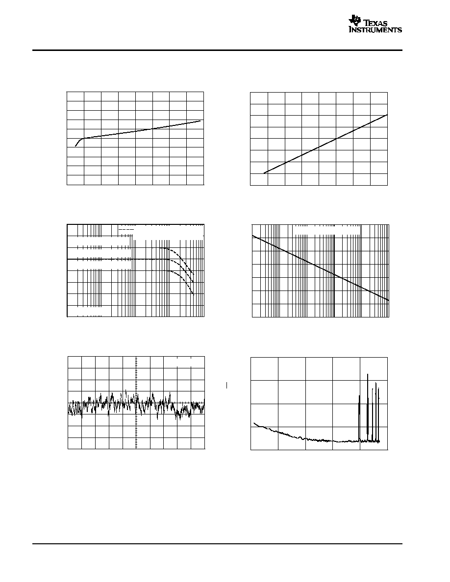
TYPICAL CHARACTERISTICS
At T
A
= +25
∞
C and V
VSP
= +24V, unless otherwise noted.
5
10
Supply Voltage (V)
QUIESCENT CURRENT vs SUPPLY VOLTAGE
45
550
530
510
490
470
450
430
410
390
370
350
Q
u
i
e
s
c
en
t
C
ur
r
e
nt
(
µ
A)
15
20
25
30
35
40
-
75
-
50
Temperature (
_
C)
QUIESCENT CURRENT vs TEMPERATURE
125
700
650
600
550
500
450
400
350
300
Q
u
i
e
s
c
en
t
C
ur
r
e
nt
(
µ
A)
-
25
0
25
50
75
100
1k
Frequency (Hz)
GAIN vs FREQUENCY
10M
40
30
20
10
0
-
10
-
20
-
30
-
40
Ga
i
n
(d
B
)
10k
100k
1M
R
SET
= 2k
, R
LOAD
= 2k
R
SET
= 2k
, R
LOAD
= 600
R
SET
= 2k
, R
LOAD
= 200
Gain = V
LOAD
/V
VIN
See Applications Information,
Dynamic Performance
10
Frequency (Hz)
POWER-SUPPLY REJECTION RATIO vs FREQUENCY
1M
140
120
100
80
60
40
20
0
PS
R
R
(
d
B
)
100
1k
10k
100k
R
SET
= 2k
, No Bypass Cap
0.1Hz to 10Hz NOISE, RTI
1
µ
V/
d
i
v
1s/div
I
OUT
= 4mA
1
Frequency (Hz)
100k
100
µ
10
µ
1
µ
100n
10n
IR
Noi
s
e
(
V
RM
S
/
Hz
)
INPUT-REFERRED NOISE SPECTRUM
I
OUT
= 2mA
10
100
1k
10k

XTR111
SBOS375 - NOVEMBER 2006
www.ti.com
5
TYPICAL CHARACTERISTICS
(continued)
At T
A
= +25
∞
C and V
VSP
= +24V, unless otherwise noted.
Nonlinearity (%)
NONLINEARITY DISTRIBUTION
Po
p
u
la
t
i
o
n
-
0.0
1
-
0.
00
9
-
0.
00
8
-
0.
00
7
-
0.
00
6
-
0.
00
5
-
0.
00
4
-
0.
00
3
-
0.
00
2
-
0.
00
1
0
0.001
0.002
0.003
0.004
0.005
0.006
0.007
0.008
0.009
0.
0
1
Gain Error (%)
GAIN ERROR DISTRIBUTION
Po
p
u
la
t
i
o
n
-
0.
1
-
0.0
9
-
0.0
8
-
0.0
7
-
0.0
6
-
0.0
5
-
0.0
4
-
0.0
3
-
0.0
2
-
0.0
1
0
0.
01
0.
02
0.
03
0.
04
0.
05
0.
06
0.
07
0.
08
0.
09
0.1
-
75
-
50
Temperature (
_
C)
NONLINEARITY vs TEMPERATURE
125
0.03
0.02
0.01
0
-
0.01
-
0.02
-
0.03
N
o
n
l
i
nea
r
i
t
y
(
%
)
-
25
0
25
50
75
100
0.1mA to 25mA
4mA to 20mA
Nonlinearity Drift (ppm/
_
C)
NONLINEARITY DRIFT DISTRIBUTION
(I
OUT
= 0.1mA to 25mA; T =
-
55
_
C to +125
_
C)
0
P
o
pu
l
a
t
i
on
0.5
1.0
1.5
2.0
2.5
3.0
3.5
4.0
4.5
5.0
-
75
-
50
Temperature (
_
C)
GAIN ERROR vs TEMPERATURE
125
0.15
0.10
0.05
0
-
0.05
-
0.10
-
0.15
G
a
i
n
E
rro
r
(
%
)
-
25
0
25
50
75
100
4mA to 20mA
0.1mA to 25mA
Gain Error Drift (ppm/
_
C)
GAIN ERROR DRIFT DISTRIBUTION
(I
OUT
= 0.1mA to 25mA; T =
-
55
_
C to +125
_
C)
-
10
P
opu
l
a
t
i
on
-
9
-
8
-
7
-
6
-
5
-
4
-
3
-
2
-
1
0

XTR111
SBOS375 - NOVEMBER 2006
www.ti.com
6
TYPICAL CHARACTERISTICS
(continued)
At T
A
= +25
∞
C and V
VSP
= +24V, unless otherwise noted.
4
I
OUT
(mA)
TYPICAL NONLINEARITY
(2pt Calibration at 4mA and 20mA)
20
0.0020
0.0015
0.0010
0.0005
0.000
-
0.0005
-
0.0010
-
0.0015
-
0.0020
N
o
n
lin
e
a
r
i
t
y
(
%
)
8
12
16
0
5
10
15
20
I
OUT
(mA)
TYPICAL NONLINEARITY
(2pt Calibration at 0.1mA and 25mA)
25
0.0020
0.0015
0.0010
0.0005
0.000
-
0.0005
-
0.0010
-
0.0015
-
0.0020
N
o
n
l
i
n
e
a
ri
t
y
(%
)
0
5
I
OUT
(mA)
TYPICAL NONLINEARITY
(2pt Calibration at 0.1mA and 36mA)
40
0.010
0.008
0.006
0.004
0.002
0.000
-
0.002
-
0.004
-
0.006
-
0.008
-
0.010
N
o
n
lin
e
a
r
i
t
y
(
%
)
10
15
20
25
30
35
Seven Typical Units Shown
-
75
-
50
Temperature (
_
C)
INPUT VOLTAGE RANGE LIMIT TO THE
POSITIVE SUPPLY vs TEMPERATURE
125
3.0
2.9
2.8
2.7
2.6
2.5
2.4
2.3
2.2
2.1
2.0
Inpu
t
V
ol
t
a
g
e
R
ange
L
i
mi
t
V
VS
P
-
V
VIN
(V
)
-
25
0
25
50
75
100
V
VSP
= 12V
0
5
Output Current (mA)
OUTPUT SWING OF THE VOLTAGE ON IS PIN (V
IS
)
vs OUTPUT CURRENT
40
3.0
2.5
2.0
1.5
1.0
0.5
0
V
VSP
-
V
IS
(V
)
10
15
20
25
30
35
-
75
-
50
Temperature (
_
C)
OUTPUT SWING OF THE VOLTAGE ON IS PIN (V
IS
)
vs TEMPERATURE
125
1.8
1.7
1.6
1.5
1.4
1.3
1.2
1.1
1.0
V
VSP
-
V
IS
(V
)
-
25
0
20mA
10mA
4mA
25
50
75
100

XTR111
SBOS375 - NOVEMBER 2006
www.ti.com
7
TYPICAL CHARACTERISTICS
(continued)
At T
A
= +25
∞
C and V
VSP
= +24V, unless otherwise noted.
Input Offset Voltage (mV)
INPUT OFFSET VOLTAGE DISTRIBUTION
P
o
pu
l
a
t
i
on
-
1
-
0.
9
-
0.
8
-
0.
7
-
0.
6
-
0.
5
-
0.
4
-
0.
3
-
0.
2
-
0.
1
0
0.
1
0.
2
0.
3
0.
4
0.
5
0.
6
0.
7
0.
8
0.
9
1
Mo
r
e
V
OS
Drift (
µ
V/
_
C)
INPUT OFFSET VOLTAGE DRIFT DISTRIBUTION
-
5
Po
p
u
l
a
t
i
o
n
-
4
-
3
-
2
-
1
0
1
2
3
4
5
6
0
Supply Voltage (V)
INPUT OFFSET VOLTAGE vs SUPPLY VOLTAGE
50
100
80
60
40
20
0
-
20
-
40
-
60
-
80
-
100
In
pu
t
O
ff
s
e
t
V
o
l
t
a
ge
(
µ
V)
10
20
30
40
-
75
-
50
Temperature (
_
C)
AMPLIFIER INPUT BIAS CURRENT vs TEMPERATURE
125
30
28
26
24
22
20
18
16
14
12
10
I
n
pu
t
B
i
a
s
C
ur
r
e
nt
(
n
A
)
-
25
0
25
50
75
100
Current Limit (mA)
OUTPUT CURRENT LIMIT DISTRIBUTION
P
opu
l
a
ti
o
n
36
37
38
39
40
41
42
43
44
45
46
47
48
49
50
51
52
53
54
55
56
-
75
-
50
Temperature (
_
C)
OUTPUT CURRENT LIMIT vs TEMPERATURE
125
50
49
48
47
46
45
44
43
42
41
40
C
u
r
r
e
n
t
L
im
it
(
m
A)
-
25
0
25
50
75
100

XTR111
SBOS375 - NOVEMBER 2006
www.ti.com
8
TYPICAL CHARACTERISTICS
(continued)
At T
A
= +25
∞
C and V
VSP
= +24V, unless otherwise noted.
Regulator Voltage (V)
REGULATOR VOLTAGE DISTRIBUTION
I
LOAD
= 0.6mA
P
opul
ati
o
n
2.
8
5
0
2.
8
6
5
2.
8
8
0
2.
8
9
5
2.
9
1
0
2.
9
2
5
2.
9
4
0
2.
9
5
5
2.
9
7
0
2.
9
8
5
3
3.
0
1
5
3.
0
3
0
3.
0
4
5
3.
0
6
0
3.
0
7
5
3.
0
9
0
3.
1
0
5
3.
1
2
0
3.
1
3
5
3.
1
5
0
Regulator Voltage Drift (ppm/
_
C)
REGULATOR VOLTAGE DRIFT DISTRIBUTION
0
P
opu
l
a
t
i
on
10
I
LOAD
= 0.6mA
20
30
40
50
60
70
80
M ore
V
REGS
Input Bias Current (
µ
A)
REGULATOR INPUT BIAS CURRENT DISTRIBUTION
(Current into REGS Pin)
Po
p
u
l
a
t
i
o
n
-
4.
0
-
3.
6
-
3.
2
-
2.
8
-
2.
4
-
2.
0
-
1.
6
-
1.
2
-
0.
8
-
0.
4
0
0.
4
0.
8
1.
2
1.
6
2.
0
2.
4
2.
8
3.
2
3.
6
4.
0
V
REGS
Input Bias Current Drift (nA/
_
C)
REGULATOR INPUT BIAS CURRENT
DRIFT DISTRIBUTION (Drift of Current into REGS Pin)
0
P
o
pul
a
t
i
o
n
0.5
1.0
1.5
2.0
2.5
3.0
3.5
4.0
4.5
5.0
0
5
Supply Voltage (V)
REGULATOR VOLTAGE vs SUPPLY VOLTAGE
50
3.05
3.04
3.03
3.02
3.01
3.00
2.99
2.98
2.97
2.96
2.95
R
egu
l
a
t
o
r
V
o
l
tage
(
V
)
10
15
20
25
30
35
40
45
I
LOAD
= 0.6mA
-
75
-
50
Temperature (
_
C)
REGULATOR VOLTAGE vs TEMPERATURE
125
3.05
3.04
3.03
3.02
3.01
3.00
2.99
2.98
2.97
2.96
2.95
R
egu
l
a
t
o
r
V
ol
t
age
(
V
)
-
25
0
25
50
75
100
I
LOAD
= 0.6mA

XTR111
SBOS375 - NOVEMBER 2006
www.ti.com
9
TYPICAL CHARACTERISTICS
(continued)
At T
A
= +25
∞
C and V
VSP
= +24V, unless otherwise noted.
STEP RESPONSE: V
FS
= 4V, R
SET
= 2k
, R
LD
= 600
(Rising Edge Depends on C
GATE
at VG Pin)
5V/div
5V/div
10
µ
s/div
Photo taken with C
GATE
= 130pF
STEP RESPONSE: V
FS
= 2.5V, R
SET
= 1.25k
, R
LD
= 600
(Rising Edge Depends on C
GATE
at VG Pin)
10V/div
2V/div
10
µ
s/div
Photo taken with C
GATE
= 130pF
REGULATOR LOAD TRANSIENT
(V
REG
Gain = 1V, V
REGF
= 3V, C
L
= 470nF
I
LOAD
= 3mA
±
0.3mA)
10mV/div
1V/div
40
µ
s/div
REGULATOR LOAD TRANSIENT
(V
REG
Gain = 4V, V
REGF
= 12V, C
L
= 470nF,
I
LOAD
= 3mA
±
0.3mA)
2V/div
10mV/div
40
µ
s/div
-
75
-
50
Temperature (
_
C)
MAXIMUM REGULATOR CURRENT vs TEMPERATURE
125
29
27
25
23
21
19
17
15
M
a
x
i
mum
R
egu
l
a
t
o
r
O
u
t
put
C
u
r
r
ent
(
m
A
)
-
25
0
25
50
75
100

XTR111
SBOS375 - NOVEMBER 2006
www.ti.com
10
APPLICATION INFORMATION
The XTR111 is a voltage-controlled current source capa-
ble of delivering currents from 0mA to 36mA. The primary
intent of the device is to source the commonly-used indus-
trial current ranges of 0mA-20mA or 4mA-20mA. The per-
formance is specified for a supply voltage of up to 40V. The
maximum supply voltage is 44V. The voltage-to-current ra-
tio is defined by an external resistor, R
SET
; therefore, the in-
put voltage range can be freely set in accordance with the
application requirement. The output current is cascoded
by an external P-Channel MOSFET transistor for large
voltage compliance extending below ground, and for easy
power dissipation. This arrangement ensures excellent
suppression of typical interference signals from the indus-
trial environment because of the extremely high output im-
pedance and wide voltage compliance.
An error detection circuit activates a logic output (error
flag) in case the output current cannot correctly flow. It indi-
cates a wire break, high load resistor, or loss of headroom
for the current output to the positive supply.
The output disable (OD) provided can be used during pow-
er-on, multiplexing and other conditions where the output
should present no current. It has an internal pull-up that
causes the XTR111 to come up in output disable mode un-
less the OD pin is tied low.
The onboard voltage regulator can be adjusted between
3V to 15V and delivers up to 5mA load current. It is in-
tended to supply signal conditioning and sensor excitation
in 3-wire sensor systems. Voltages above 3V can be set
by a resistive divider.
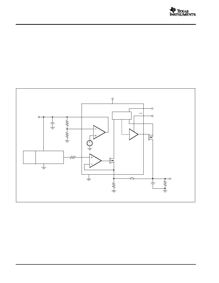
Figure 1 shows a basic connection for the XTR111. The in-
put voltage V
VIN
reappears across R
SET
and controls 1/10
of the output current. The I-Mirror has a precise current
gain of 10. This configuration leads to the transfer function:
I
OUT
= 10
∑
(V
VIN
/R
SET
)
The output of the voltage regulator can be set over the
range of 3V to 12V by selecting R
1
and R
2
using the follow-
ing equation.
V
REGF
= 3V
∑
(R
1
+ R
2
)/R
2
3V
REGF
REGS
5V
Signal
Source
(Sensor or
DAC, for
example)
V
VSP
= 24V Supply
I-Mirror
VSP
1
9
8
2
3
S
D
G
VG
IS
Q
EXT
P-Channel
MOSFET
(Pull Low for Normal Operation)
0mA or 4mA to 20mA
OD
EF
C
1
R
2
8.2k
VIN
6
4
5
R
SET
SET
7
10
GND
R
1
5.6k
V
OUT
Load
I
OUT
(
±
Load Ground)
I
OUT
= 10
(
)
V
VIN
R
SET
Figure 1. Basic Connection for 0mA to 20mA Related to 0V to 5V Signal Input. The Voltage Regulator is
Set to 5V Output.

XTR111
SBOS375 - NOVEMBER 2006
www.ti.com
11
EXPLANATION OF PIN FUNCTIONS
VIN: This input is a conventional, noninverting, high-
impedance input of the internal operational amplifier
(OPA). The internal circuitry is protected by clamp diodes
to supplies. An additional clamp connected to
approximately 18V protects internal circuitry. Place a small
resistor in series with the input to limit the current into the
protection if voltage can be present without the XTR111
being powered. Consider a resistor value equal to R
SET
for
bias current cancellation.
SET: The total resistance connected between this pin and
VIN reference sets the transconductance. Additional
series resistance can degrade accuracy and drift. The
voltage on this pin must not exceed 14V because this pin
is not protected to voltages above this level.
IS: This output pin is connected to the transistor source of
the external FET. The accuracy of the output current to IS
is achieved by dynamic error correction in the current
mirror. This pin should never be pulled more than 6.5V
below the positive supply. An internal clamp is provided to
protect the circuit, but it must be current-limited externally
to less than 25mA.
VG: The gate drive for the external FET is protected
against shorts to the supply and GND. The circuit is
clamped so that it will not drive more than 18V below the
positive supply. The external FET should be protected if its
gate could be externally pulled beyond its ratings.
REGF: The output of the regulator buffer can source up to
5mA current, but has very limited (less than 50
µ
A) sinking
capability. The maximum short-circuit current is in the
range of 15mA to 25mA, changing over temperature.
REGS: This pin is the sense input of the voltage regulator.
It is referenced to an internal 3V reference circuit. The input
bias current can be up to 2
µ
A. Avoid capacitive loading of
REGS that may compromise the loop stability of the
voltage regulator.
VSP: The supply voltage of up to a maximum of 44V allows
operation in harsh industrial environment and provides
headroom for easy protection against over-voltage. Use a
large enough bypass capacitor (> 100nF) and eventually
a damping inductor or a small resistor (5
) to decouple the
XTR111 supply from the noise typically found on the 24V
supplies.
EF: The active low error flag (logic output) is intended for
use with an external pull-up to logic-high for reliable
operation when this output is used. However, it has a weak
internal pull-up to 5V and can be left unconnected if not
used.
OD: This control input has a 4
µ
A internal pull-up disabling
the output. A pull-down or short to GND is required to
activate the output. Controlling OD reduces output glitches
during power-on and power-off. This logic input controls
the output. If not used, connect to GND.
The regulator is not affected by OD.

XTR111
SBOS375 - NOVEMBER 2006
www.ti.com
12
EXTERNAL MOSFET
The XTR 111 delivers the precise output current to the IS
pin. The voltage at this pin is normally 1.4V below V
VSP
. It
must not fall more than 5.5V below V
VSP
.
This output requires an external transistor (Q
EXT
) that
forms a cascode for the current output. The resistor must
be rated for the maximum possible voltage on V
OUT
and
must dissipate the power generated by the current and the
voltage across it.
The gate drive (VG) can drive from close to the positive
supply rail to 16V below the positive supply voltage (V
VSP
).
Most modern MOSFETs accept a maximum V
GS
of 20V. A
protection clamp is only required if a large drain gate ca-
pacitance can pulse the gate beyond the rating of the
MOSFET. Pulling the OD pin high disables the gate driver
and closes a switch connecting an internal 3k
resistor
from the VSP pin to the VG pin. This resistor discharges
the gate of the external FET and closes the channel; see
Figure 2.
Table 1 lists some example devices in SO-compatible
packages, but other devices can be used as well. Avoid ex-
ternal capacitance from IS. This capacitance could be
compensated by adding additional capacitance from VG
to IS; however, this compensation may slow the output
down.
The drain-to-source breakdown voltage should be se-
lected high enough for the application. Surge voltage
protection might be required for negative over-voltages.
For positive over-voltages, a clamp diode to the 24V sup-
ply is recommended, protecting the FET from reversing.
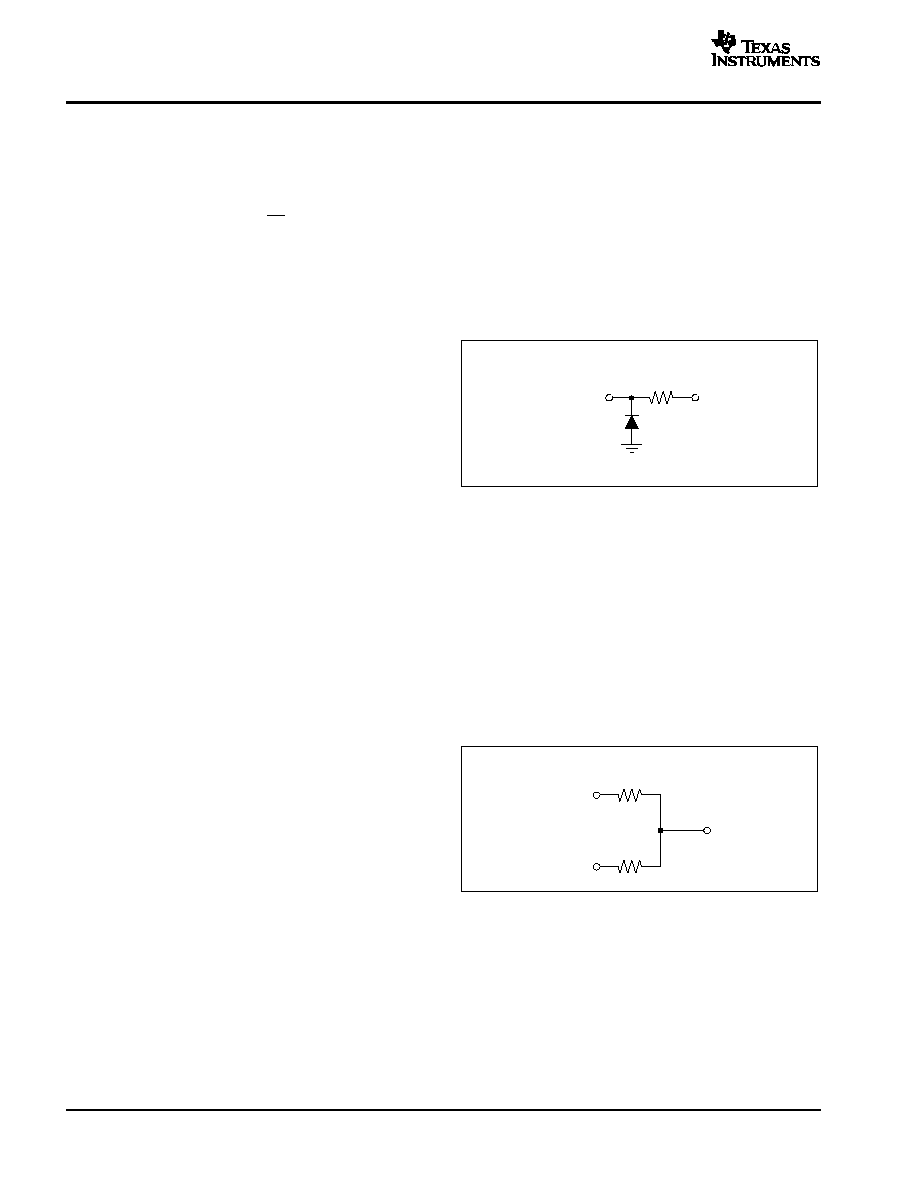
VSP
VG
OD
Switch
3k
16V
GND
Figure 2. Equivalent Circuit for Gate Drive and
Disable Switch
Table 1. P-Channel MOSFET (Examples)
(1)
MANUFACTURER
PART NO.
BREAKDOWN VGS
PACKAGE
C-GATE
Infineon
BSP170P
-60V
SOT-223
328pF
International Rectifier
IRFL9014
-60V
SOT-223
270pF
NEC
2SJ326-Z
-60V
Spec.
320pF
ON Semiconductor
NTF2955
-60V
SOT-223
492pF
Supertex Inc.
TP2510
-100V
TO-243AA
80pF
(1) Data from published product data sheet; not ensured.

XTR111
SBOS375 - NOVEMBER 2006
www.ti.com
13
DYNAMIC PERFORMANCE
The rise time of the output current is dominated by the gate
capacitance of the external FET.
The accuracy of the current mirror relies on the dynamic
matching of multiple individual current sources. Settling to
full resolution may require a complete cycle lasting around
100
µ
s. Figure 3 shows an example of the ripple generated
from the individual current source values that average to
the specified accuracy over the full cycle.
The output glitch magnitude depends on the mismatch of
the internal current sources. It is approximately
proportional to the output current level and scales directly
with the load resistor value. It will slightly differ from part to
part.
50
m
V
/
d
i
v
20
µ
s/div
500
External FET
No Filter
Figure 3. Output Noise without Filter into 500
500
C
F
10nF
External FET
Load Capacitor
50m
V
/
di
v
20
µ
s/div
Figure 4. Output with 10nF Parallel to 500
500
C
F
10nF
External FET
Typical Filter
R
F
10k
NOTE: Scale has been changed
from Figure 3 and Figure 4.
5m
V/
di
v
20
µ
s/div
Figure 5. Output with Additional Filter
XTR111
SBOS375 - NOVEMBER 2006
www.ti.com
14
OUTPUT ERROR FLAG AND DISABLE INPUT
The XTR111 has additional internal circuitry to detect an
error in the output current. In case the controlled output
current cannot flow due to a wire break, high load
resistance or the output voltage level approaching the
positive supply, the error flag (EF), an open drain logic
output, pulls low. When used, this digital output requires
external pull-up to logic high (the internal pull-up current is
2
µ
A).
The output disable (OD) is a logic input with approximately
4
µ
A of internal pull-up to 5V. The XTR111 comes up with
the output disabled until the OD pin is pulled low. Logic
high disables the output to zero output current. It can be
used for calibration, power-on and power-off glitch
reduction and for output multiplexing with other outputs
connected to the same terminal pin.
Power-on while the output is disabled (OD = high) cannot
fully suppress output glitching. While the supply voltage
passes through the range of 3V to 4V, internal circuits turn
on. Additional capacitance between pins VG and IS can
suppress the glitch. The smallest glitch energy appears
with the OD pin left open; for practical use, however, this
pin can be driven high through a 10k
resistor before the
24V supply is applied, if logic voltage is available earlier.
Alternatively, an open drain driver can control this pin using
the internal pull-up current. Pull-up to the internal regulator
tends to increase the energy because of the delay of the
regulator voltage increase, again depending on the supply
voltage rise time for the first few volts.
INPUT VOLTAGE
The input voltage range for a given output current span is
set by R
SET
according to the transfer function. Select a
precise and low drift resistor for best performance,
because resistor drift directly converts into drift of the
output current. Careful layout must also minimize any
series resistance with R
SET
and the VIN reference point.
The input voltage is referred to the grounding point of R
SET
.
Therefore, this point should not be distorted from other
currents. Assuming a 5V full-scale input signal for a 20mA
output current, R
SET
is 2.5k
. A resistance uncertainty of
just 2.5
already degrades the accuracy to below 0.1%.
The linear input voltage range extends from 0V to 12V, or
2.3V below the positive supply voltage (whichever is
smaller). The lowest rated supply voltage accomodates
an input voltage range of up to 5V. Potential clipping is not
detected by an error signal; therefore, safe design guard
banding is recommended.
Do not drive the input negative (referred to GND) more
than 300mV. Higher negative voltages turn on the internal
protection diodes. Insert a resistor in series with the input
if negative signals can occur eventually during power-on
or -off or during other transient conditions. Select a resistor
value limiting the possible current to 0.3mA. Higher
currents are non-destructive (see Absolute Maximum
Ratings), but they can produce output current glitches
unless in disable mode.
More protection against negative input signals is provided
using a standard diode and a 2.2k
resistor, as shown in
Figure 6.
VIN
1N4148
V-Signal
2.2k
Figure 6. Enhanced Protection Against Negative
Overload of V
IN
4mA-20mA OUTPUT
The XTR111 does not provide internal circuits to generate
4mA with 0V input signal. The most common way to shift
the input signal is a two resistor network connected to a
voltage reference and the signal source, as shown in
Figure 7. This arrangement allows easy adjustment for
over-and under-range. The example assumes a 5V
reference (V
REF
) that equals the full-scale signal voltage
and a signal span of 0V to 5V for 4mA to 20mA (I
MIN
to I
MAX
)
output.
VIN
1V to 5V
R
1
40k
Input Voltage
0V to 5V
Reference
Voltage
5V
R
2
10k
Figure 7. Resistive Divider for I
MIN
to I
MAX
Output
(4mA to 20mA) with 0 to V
FS
Signal Source
The voltage regulator output or a more precise reference
can be used as V
REF
. Observe the potential drift added by
the drift of the resistors and the voltage reference.

XTR111
SBOS375 - NOVEMBER 2006
www.ti.com
15
LEVEL SHIFT OF 0V INPUT AND
TRANSCONDUCTANCE TRIM
The XTR111 offers low offset voltage error at the input,
which normally does not require cancellation. If the signal
source cannot deliver 0V in a single-supply circuit, an
additional resistor from the SET pin to a positive reference
voltage or the regulator output (Figure 8) can shift the zero
level for the input (V
IN
) to a positive voltage. Therefore, the
signal source can drive this value within a positive voltage
range. The example shows a +100mV (102.04mV) offset
generated to the signal input. The larger this offset,
however, the more influence of its drift and inaccuracy is
seen in the output signal. The voltage at SET should not
be larger than 12V for linear operation
Transconductance (the input voltage to output current
ratio) is set by R
SET
. The desired resistor value may be
found by choosing a combination of two resistors.
VOLTAGE REGULATOR
The externally adjustable voltage regulator provides up to
5mA of current. It offers drive (REGF) and sense (REGS)
to allow external setting of the output voltage as shown in
Figure 9. The sense input (REGS) is referenced to 3.0V
representing the lowest adjustable voltage level. An
external resistor divider sets V
REGF
.
V
REGF
= V
REGS
∑
(R
1
+ R
2
)/R
2
Table
2 provides example values for the regulator
adjustment resistors.
Table 2. Examples for the Resistor Values Setting
the Regulator Voltage
V
REGF
(1)
R
1
R
2
3V
0
3.3V
3.3k
33k
5V
5.6k
8.2k
12.4V
27k
8.6k
(1) Values have been rounded.
R
SET
2k
VIN
SET
+100mV
Offset
120k
5V
Reference
I-V Amp
XTR111
Figure 8. Input Voltage Level Shift for 0mA
Output Current
3V
470nF
REGF
(a)
(b)
REGS
3V
3V
470nF
REGF
REGS
R
1
5.6k
REG
V
REG
R
2
8.2k
3V
470nF
REGF
REGS
R
1
5.6k
V
REG
V
SP
220
R
2
8.2k
1k
1k
3V
REGF
REGS
R
3
47k
5V
Source
(c)
(d)
Figure 9. Basic Connections of the Voltage Regulator
XTR111
SBOS375 - NOVEMBER 2006
www.ti.com
16
The voltage at REGF is limited by the supply voltage. If the
supply voltage drops close to the set voltage, the driver
output saturates and follows the supply with a voltage drop
of less than 1V (depending on load current and
temperature).
For good stability and transient response, use a load
capacitance of 470nF or larger. The bias current into the
sense input (REGS) is typically less than 1
µ
A. This current
should be considered when selecting high resistance
values for the voltage setting because it lowers the voltage
and produces additional temperature dependence.
The REGF output cannot sink current. In case of supply
voltage loss, the output is protected against the discharge
currents from load capacitors by internal protection
diodes; the peak current should not exceed 25mA.
If the voltage regulator output is not used, connect REGF
to REGS (the 3V mode) loaded with a 2.2nF capacitor.
Alternatively, overdrive the loop pulling REGS high (see
Figure 9d).
APPLICATION BLOCK DIAGRAMS
12-Bit Digital-to-Analog
Converter
DAC7551
Digital I/O
Current
Mirror
VSP
VG
IS
Q
1
3
S
D
G
2
8
9
EF
OD
R
S ET
2.5k
SET
6
7
10
VIN
GND
4
5
1
SW1
0mA to 20mA or
0V to 5V Output
Switch for current
or voltage output
R
3
2.5k
C
2
470nF
R
1
2k
REGF
REGS
3V
5V
R
2
3k
C
L O A D
R
LO AD
Figure 10. Current or Voltage Output (SW1) Using 0V to 5V Input from a 12-Bit Digital-to-Analog
Converter DAC7551

XTR111
SBOS375 - NOVEMBER 2006
www.ti.com
17
16-Bit Digital-to- Analog
Converter
DAC8551
Digital I/O
Current
Mirror
IS
2
8
9
EF
OD
R
SE T
2k
(1.995k
)
NOTE: Calculate R
SE T
for R
4
Parallel to R
S ET
.
SET
6
7
10
VIN
GND
4
5
0mA to 20mA output
for 10mV to 4096mV input
or a code of 160b to 65536b
R
3
2k
R
4
817.2k
R
1
2k
REGF
REGS
3V
R
2
3k
REF3040
4096mV
Voltage Reference
1
VSP
C
2
470nF
5V
C
LO AD
R
L OA D
Load
VG
Q
1
3
S
D
G
Figure 11. Precision Current Output with Signal from 16-Bit DAC. Input Offset Shifted (R4) by 10mV for
Zero Adjustment Range
16-Bit Digital-to- Analog
Converter
DAC8551
Digital I/O
Current
Mirror
IS
2
8
9
EF
OD
R
SE T
2k
(1.995k
)
NOTE: Calculate R
SE T
for R
4
Parallel to R
S ET
.
SET
6
7
10
VIN
GND
4
5
0mA to 20mA output
for 10mV to 4096mV input
or a code of 160b to 65536b
R
3
2k
R
4
817.2k
R
1
2k
REGF
REGS
3V
R
2
3k
REF3040
4096mV
Voltage Reference
1
VSP
C
2
470nF
5V
C
LO AD
R
L OA D
Load
VG
Q
1
3
S
D
G
Figure 12. 0V to 10V or 0mA to 20mA Output Selected by Jumper (SW1)

XTR111
SBOS375 - NOVEMBER 2006
www.ti.com
18
16-Bit Digital-to- Analog
Converter
DAC8551
Digital I/O
Current
Mirror
IS
2
8
9
EF
OD
R
SE T
2k
(1.995k
)
NOTE: Calculate R
SE T
for R
4
Parallel to R
S ET
.
SET
6
7
10
VIN
GND
4
5
0mA to 20mA output
for 10mV to 4096mV input
or a code of 160b to 65536b
R
3
2k
R
4
817.2k
R
1
2k
REGF
REGS
3V
R
2
3k
REF3040
4096mV
Voltage Reference
1
VSP
C
2
470nF
5V
C
LO AD
R
L OA D
Load
VG
Q
1
3
S
D
G
Figure 13. 2-Wire 4mA to 20mA Current Loop Driver with Adjustable Voltage Regulator
0V to 2V
Input
Current
Mirror
VG
IS
Q
1
3
2
8
9
EF
OD
1
VSP
R
SE T
50.251
R
4
150k
SET
GND
6
7
10
VIN
4
5
3V Supply
GI
R
3
25k
REGF
REGS
3V
GI
GI
R
5
10k
NOTE: Input voltage range is set by the four external resistors. Q
1
can be a FET or a PNP transistor. Internal GND reference is GI.
2-Wire
4mA to 20mA
Output
S
D
G
Figure 14. 2-Wire 4mA to 20mA Current Loop Driver for 0V to 2V Signal Input
XTR111
SBOS375 - NOVEMBER 2006
www.ti.com
19
C
2
470nF
REGS
NOTE: (1) Resistor R
4
can be calculated to protect Q
2
from overcurrent in fault conditions.
REGF
3V
R
3
1k
C
2
470nF
REGS
REGF
6V
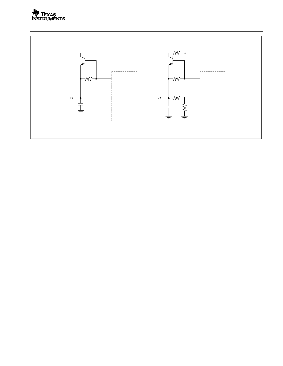
+24V
Q2
NPN
Q2
NPN
(a)
(b)
R
3
1k
R
4
(1)
100
R
1
10k
R
2
10k
Figure 15. Voltage Regulator Current Boost Using a Standard NPN Transistor
PACKAGE AND HEAT SINKING
The dominant portion of power dissipation for the current
output is in the external FET.
The XTR111 only generates heat from the supply voltage
with the quiescent current, the internal signal current that
is 1/10 of the output current and the current and internal
voltage drop of the regulator.
The exposed thermal pad on the bottom of the XTR111
package allows excellent heat dissipation of the device
into the printed circuit board (PCB).
THERMAL PAD
The thermal pad must be connected to the same voltage
potential as the device GND pin.
Packages with an exposed thermal pad are specifically
designed to provide excellent power dissipation, but board
layout greatly influences overall heat dissipation. The
thermal resistance from junction-to-ambient (T
JA
) is
specified for the packages with the exposed thermal pad
soldered to a normalized PCB, as described in Technical
Brief SLMA002, PowerPAD Thermally-Enhanced
Package. See also EIA/JEDEC Specifications JESD51-0
to 7, QFN/SON PCB Attachment (SLUA271), and Quad
Flatpack No-Lead Logic Packages (SCBA017). These
documents are available for download at www.ti.com.
NOTE: All thermal models have an accuracy 20%.
Component population, layout of traces, layers, and air
flow strongly influence heat dissipation. Worst-case load
conditions should be tested in the real environment to
ensure proper thermal conditions. Minimize thermal stress
for proper long-term operation with a junction temperature
well below +125
∞
C.
LAYOUT GUIDELINES
The leadframe die pad should be soldered to a thermal pad
on the PCB. A mechanical data sheet showing an example
layout is attached at the end of this data sheet.
Refinements to this layout may be required based on
assembly process requirements. Mechanical drawings
located at the end of this data sheet list the physical
dimensions for the package and pad. The five holes in the
landing pattern are optional, and are intended for use with
thermal vias that connect the leadframe die pad to the
heatsink area on the PCB.
Soldering the exposed pad significantly improves
board-level reliability during temperature cycling, key
push, package shear, and similar board-level tests. Even
with applications that have low-power dissipation, the
exposed pad must be soldered to the PCB to provide
structural integrity and long-term reliability.

PACKAGING INFORMATION
Orderable Device
Status
(1)
Package
Type
Package
Drawing
Pins Package
Qty
Eco Plan
(2)
Lead/Ball Finish
MSL Peak Temp
(3)
XTR111AIDRCR
ACTIVE
SON
DRC
10
3000 Green (RoHS &
no Sb/Br)
CU NIPDAU
Level-2-260C-1 YEAR
XTR111AIDRCT
ACTIVE
SON
DRC
10
250
Green (RoHS &
no Sb/Br)
CU NIPDAU
Level-2-260C-1 YEAR
(1)
The marketing status values are defined as follows:
ACTIVE: Product device recommended for new designs.
LIFEBUY: TI has announced that the device will be discontinued, and a lifetime-buy period is in effect.
NRND: Not recommended for new designs. Device is in production to support existing customers, but TI does not recommend using this part in
a new design.
PREVIEW: Device has been announced but is not in production. Samples may or may not be available.
OBSOLETE: TI has discontinued the production of the device.
(2)
Eco Plan - The planned eco-friendly classification: Pb-Free (RoHS), Pb-Free (RoHS Exempt), or Green (RoHS & no Sb/Br) - please check
http://www.ti.com/productcontent
for the latest availability information and additional product content details.
TBD: The Pb-Free/Green conversion plan has not been defined.
Pb-Free (RoHS): TI's terms "Lead-Free" or "Pb-Free" mean semiconductor products that are compatible with the current RoHS requirements
for all 6 substances, including the requirement that lead not exceed 0.1% by weight in homogeneous materials. Where designed to be soldered
at high temperatures, TI Pb-Free products are suitable for use in specified lead-free processes.
Pb-Free (RoHS Exempt): This component has a RoHS exemption for either 1) lead-based flip-chip solder bumps used between the die and
package, or 2) lead-based die adhesive used between the die and leadframe. The component is otherwise considered Pb-Free (RoHS
compatible) as defined above.
Green (RoHS & no Sb/Br): TI defines "Green" to mean Pb-Free (RoHS compatible), and free of Bromine (Br) and Antimony (Sb) based flame
retardants (Br or Sb do not exceed 0.1% by weight in homogeneous material)
(3)
MSL, Peak Temp. -- The Moisture Sensitivity Level rating according to the JEDEC industry standard classifications, and peak solder
temperature.
Important Information and Disclaimer:The information provided on this page represents TI's knowledge and belief as of the date that it is
provided. TI bases its knowledge and belief on information provided by third parties, and makes no representation or warranty as to the
accuracy of such information. Efforts are underway to better integrate information from third parties. TI has taken and continues to take
reasonable steps to provide representative and accurate information but may not have conducted destructive testing or chemical analysis on
incoming materials and chemicals. TI and TI suppliers consider certain information to be proprietary, and thus CAS numbers and other limited
information may not be available for release.
In no event shall TI's liability arising out of such information exceed the total purchase price of the TI part(s) at issue in this document sold by TI
to Customer on an annual basis.
PACKAGE OPTION ADDENDUM
www.ti.com
16-Nov-2006
Addendum-Page 1


IMPORTANT NOTICE
Texas Instruments Incorporated and its subsidiaries (TI) reserve the right to make corrections, modifications,
enhancements, improvements, and other changes to its products and services at any time and to discontinue
any product or service without notice. Customers should obtain the latest relevant information before placing
orders and should verify that such information is current and complete. All products are sold subject to TI's terms
and conditions of sale supplied at the time of order acknowledgment.
TI warrants performance of its hardware products to the specifications applicable at the time of sale in
accordance with TI's standard warranty. Testing and other quality control techniques are used to the extent TI
deems necessary to support this warranty. Except where mandated by government requirements, testing of all
parameters of each product is not necessarily performed.
TI assumes no liability for applications assistance or customer product design. Customers are responsible for
their products and applications using TI components. To minimize the risks associated with customer products
and applications, customers should provide adequate design and operating safeguards.
TI does not warrant or represent that any license, either express or implied, is granted under any TI patent right,
copyright, mask work right, or other TI intellectual property right relating to any combination, machine, or process
in which TI products or services are used. Information published by TI regarding third-party products or services
does not constitute a license from TI to use such products or services or a warranty or endorsement thereof.
Use of such information may require a license from a third party under the patents or other intellectual property
of the third party, or a license from TI under the patents or other intellectual property of TI.
Reproduction of information in TI data books or data sheets is permissible only if reproduction is without
alteration and is accompanied by all associated warranties, conditions, limitations, and notices. Reproduction
of this information with alteration is an unfair and deceptive business practice. TI is not responsible or liable for
such altered documentation.
Resale of TI products or services with statements different from or beyond the parameters stated by TI for that
product or service voids all express and any implied warranties for the associated TI product or service and
is an unfair and deceptive business practice. TI is not responsible or liable for any such statements.
Following are URLs where you can obtain information on other Texas Instruments products and application
solutions:
Products
Applications
Amplifiers
amplifier.ti.com
Audio
www.ti.com/audio
Data Converters
dataconverter.ti.com
Automotive
www.ti.com/automotive
DSP
dsp.ti.com
Broadband
www.ti.com/broadband
Interface
interface.ti.com
Digital Control
www.ti.com/digitalcontrol
Logic
logic.ti.com
Military
www.ti.com/military
Power Mgmt
power.ti.com
Optical Networking
www.ti.com/opticalnetwork
Microcontrollers
microcontroller.ti.com
Security
www.ti.com/security
Low Power Wireless www.ti.com/lpw
Telephony
www.ti.com/telephony
Video & Imaging
www.ti.com/video
Wireless
www.ti.com/wireless
Mailing Address:
Texas Instruments
Post Office Box 655303 Dallas, Texas 75265
Copyright
2006, Texas Instruments Incorporated