
FEATURES
D
USER-SELECTABLE: Voltage or Current
Output
D
+40V SUPPLY VOLTAGE
D
V
OUT
:
±
10V (up to
±
17.5V at
±
20V supply)
D
I
OUT
:
±
20mA (linear up to
±
24mA)
D
SHORT- OR OPEN-CIRCUIT FAULT
INDICATOR PIN
D
NO CURRENT SHUNT REQUIRED
D
OUTPUT DISABLE FOR SINGLE INPUT MODE
D
THERMAL PROTECTION
D
OVER-CURRENT PROTECTION
D
SEPARATE DRIVER AND RECEIVER
CHANNELS
D
DESIGNED FOR TESTABILITY
IA
Current Copy
OPA
R
GAIN
RG
1
RG
2
I
COPY
C
C
I
DRV
I
IA
IA
IN+
IA
IN
-
Load
DRV
IA
OUT
V
IN
SET
I
MON
V
-
DGND
V+
XTR300
Digital
Control
OD
M2
M1
Error
Flags
EF
CM
EF
LD
EF
OT
(Optional)
Input Signal
V
REF
R
IA
1k
R
SET
GND1
GND3
R
OS
R
IMON
1k
GND2
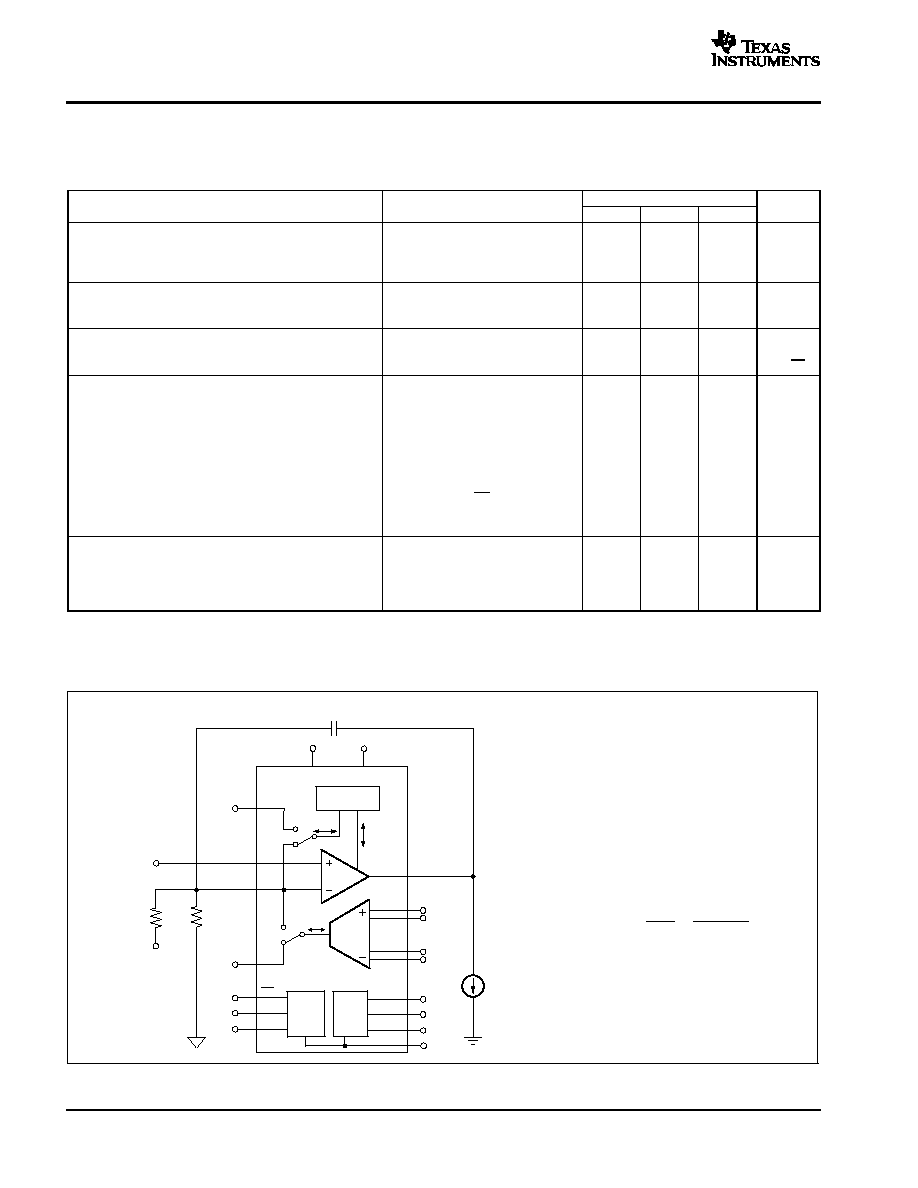
Figure 1. XTR300 Basic Diagram
APPLICATIONS
D
PLC OUTPUT PROGRAMMABLE DRIVER
D
INDUSTRIAL CROSS-CONNECTORS
D
INDUSTRIAL HIGH-VOLTAGE I/O
D
3-WIRE-SENSOR CURRENT OR VOLTAGE
OUTPUT
D
±
10V 2- AND 4-WIRE VOLTAGE OUTPUT
Patents Pending
DESCRIPTION
The XTR300 is a complete output driver for industrial and
process control applications. The output can be configured
as current or voltage by the digital I/V select pin. No
external shunt resistor is required. Only external
gain-setting resistors and a loop compensation capacitor
are required.
The separate driver and receiver channels provide
flexibility. The Instrumentation Amplifier (IA) can be used
for remote voltage sense or as a high-voltage, high-
impedance measurement channel. In voltage output
mode, a copy of the output current is provided, allowing
calculation of load resistance.
The digital output selection capability, together with the
error flags and monitor pins, make remote configuration
and troubleshooting possible. Fault conditions on the
output and on the IA input as well as over-temperature
conditions are indicated by the error flags. The monitoring
pins provide continuous feedback about load power or
impedance. For additional protection, the maximum output
current is limited and thermal protection is provided.
Digital communication like HART
can be modulated onto
the input signal. The receive signal applied to the output
can be detected at the monitor pins in both current and
voltage output modes. In addition to HART
communication, the device offers system or sensor
configuration through the signal connector.
The XTR300 is specified over the -40
∞
C to +85
∞
C
industrial temperature range and for supply voltage up to
40V.
XTR300
SBOS336B - JUNE 2005 - REVISED MARCH 2006
Industrial Analog Current/Voltage
OUTPUT DRIVER
PRODUCTION DATA information is current as of publication date. Products
conform to specifications per the terms of Texas Instruments standard warranty.
Production processing does not necessarily include testing of all parameters.
www.ti.com
Copyright
2005-2006, Texas Instruments Incorporated
Please be aware that an important notice concerning availability, standard warranty, and use in critical applications of Texas Instruments
semiconductor products and disclaimers thereto appears at the end of this data sheet.
HART is a registered trademark of the HART Communication Foundation.
All other trademarks are the property of their respective owners.

XTR300
SBOS336B - JUNE 2005 - REVISED MARCH 2006
www.ti.com
2
ABSOLUTE MAXIMUM RATINGS
(1)
Supply Voltage
+44V
. . . . . . . . . . . . . . . . . . . . . . . . . . . . . . . . . . . . .
Signal Input Terminals
Voltage
(2)
(V-) - 0.5V to (V+) + 0.5V
. . . . . . . . . . . . . . . . . . . . . .
Current
(2)
±
25mA
. . . . . . . . . . . . . . . . . . . . . . . . . . . . . . . . . . . . . .
DGND
±
25mA
. . . . . . . . . . . . . . . . . . . . . . . . . . . . . . . . . . . . . . . . . . .
Output Short Circuit
(3)
Continuous
. . . . . . . . . . . . . . . . . . . . . . . . . .
Operating Temperature
-55
∞
C to +125
∞
C
. . . . . . . . . . . . . . . . . . . . .
Storage Temperature
-55
∞
C to +125
∞
C
. . . . . . . . . . . . . . . . . . . . . . .
Junction Temperature
+150
∞
C
. . . . . . . . . . . . . . . . . . . . . . . . . . . . . . .
ESD Rating
Human Body Model
2000V
. . . . . . . . . . . . . . . . . . . . . . . . . . . . .
Charged Device Model
1000V
. . . . . . . . . . . . . . . . . . . . . . . . . . .
(1) Stresses above these ratings may cause permanent damage.
Exposure to absolute maximum conditions for extended periods
may degrade device reliability. These are stress ratings only, and
functional operation of the device at these or any other conditions
beyond those specified is not supported.
(2) Input terminals are diode-clamped to the power-supply rails.
Input signals that can swing more than 0.5V beyond the supply
rails should be current limited.
(3) See the Driver Output Disable section in Application Information
section for thermal protection.
PIN CONFIGURATION
Top View
QFN
M2
M1
V
IN
SET
I
MON
Pad
V+
NC
DRV
NC
V
-
1
2
3
4
5
15
14
13
12
11
IA
OU
T
IA
IN
-
IA
IN
+
RG
1
RG
2
OD
EF
OT
EF
LD
EF
CM
DG
N
D
Exposed
Thermal
Die Pad
on
Underside.
(Must be
connected
to V
-
)
6
7
8
9
10
20
19
18
17
16
This integrated circuit can be damaged by ESD. Texas
Instruments recommends that all integrated circuits be
handled with appropriate precautions. Failure to observe
proper handling and installation procedures can cause damage.
ESD damage can range from subtle performance degradation to
complete device failure. Precision integrated circuits may be more
susceptible to damage because very small parametric changes could
cause the device not to meet its published specifications.
ORDERING INFORMATION
(1)
PRODUCT
PACKAGE-LEAD
PACKAGE
DESIGNATOR
PACKAGE
MARKING
XTR300
QFN-20
(5mm x 5mm)
RGW
XTR300
(1) For the most current package and ordering information, see the
Package Option Addendum at the end of this document, or see
the TI web site at www.ti.com.
PIN ASSIGNMENTS
PIN
NAME
FUNCTION
1
M2
Mode Input
2
M1
Mode Input
3
V
IN
Noninverting Signal Input
4
SET
Input for Gain Setting; Inverting Input
5
I
MON
Current Monitor Output
6
IA
OUT
Instrumentation Amplifier Signal Output
7
IA
IN-
Instrumentation Amplifier Inverting Input
8
IA
IN+
Instrumentation Amplifier Noninverting Input
9
RG1
Instrumentation Amplifier Gain Resistor
10
RG2
Instrumentation Amplifier Gain Resistor
11
V-
Negative Power Supply
12
NC
No Internal Connection
13
DRV
Operational Amplifier Output
14
NC
No Internal Connection
15
V+
Positive Power Supply
16
DGND
Ground for Digital I/O
17
EF
CM
Error Flag for Common-Mode Over-Range,
Active Low
18
EF
LD
Error Flag for Load Error, Active Low
19
EF
OT
Error Flag for Over Temperature, Active Low
20
OD
Output Disable, Disabled Low
Pad
Pad
Exposed thermal pad must be connected to V-

XTR300
SBOS336B - JUNE 2005 - REVISED MARCH 2006
www.ti.com
3
ELECTRICAL CHARACTERISTICS: VOLTAGE OUTPUT MODE
Boldface limits apply over the temperature range, T
A
= -40
∞
C to +85
∞
C.
All specifications at T
A
= +25
∞
C, V
S
=
±
20V, R
LOAD
= 800
, R
SET
= 2k
, R
OS
= 2k
, V
REF
= 4V, R
GAIN
= 10k
, Input Signal Span 0V to 4V, and C
C
= 100pF, unless
otherwise noted.
XTR300
PARAMETER
CONDITION
MIN
TYP
MAX
UNITS
OFFSET VOLTAGE
Offset Voltage, RTI
V
OS
±
0.4
±
1.9
mV
vs Temperature
dV
OS/dT
±
1.6
±
6
µ
V/
∞
C
vs Power Supply
PSRR
V
S
=
±
5V to
±
22V
±
0.2
±
10
µ
V/V
INPUT VOLTAGE RANGE
Nominal Setup for
±
10V Output
See Figure 2
Input Voltage For Linear Operation
(V-) + 3V
(V+) - 3V
V
NOISE
Voltage Noise, f = 0.1Hz to 10Hz, RTI
3
µ
V
PP
Voltage Noise Density, f = 1kHz, RTI
e
n
40
nV/
Hz
OUTPUT
Voltage Output Swing from Rail
I
DRV
15mA
(V-) +3V
(V+) - 3
V
Gain Nonlinearity
±
0.01
±
0.1
%FS
vs Temperature
±
0.1
±
1
ppm/
∞
C
Gain Error
I
B
±
0.04
±
0.1
%FS
vs Temperature
±
0.2
±
1
ppm/
∞
C
Output Impedance, dV
DRV
/dI
DRV
7
m
Output Leakage Current While Output Disabled
Pin OD = L
(1)
30
nA
Short-Circuit Current
I
SC
±
15
±
20
±
24
mA
Capacitive Load Drive
C
LOAD
C
C
= 10nF, R
C
= 15
(2)
1
µ
F
Rejection of Voltage Difference between GND1 and GND2, RTO
130
dB
FREQUENCY RESPONSE
Bandwidth
-3dB
G = 5
300
kHz
Slew Rate
(2)
SR
1
V/
µ
s
SR
C
C
= 10nF, C
L
= 1
µ
F, R
C
= 15
0.015
V/
µ
s
Settling Time
(2)(3)
, 0.1%, Small Signal
V
DRV
=
±
1V
8
µ
s
Overload Recovery Time
50% Overdrive
12
µ
s
(1) Output leakage includes input bias current of INA.
(2) Refer to Driving Capacitive Loads section in Application Information.
(3) 8
µ
s plus number of chopping periods. See Application Information section, Internal Current Sources and Settling Time.
IA
Cu rrent C opy
OPA
R
GAIN
V
OUT
=
(
)
Transfer Function:
+
R
G
2
V
IN
R
SET
V
IN
-
V
REF
R
OS
R G
1
R G
2
I
COPY
C
C
I
DRV
I
IA
IA
IN+
IA
IN
-
Load
D RV
IA
OUT
V
IN
S ET
I
MON
V
-
D GN D
V +
X TR3 00
D igital
C ontro l
OD
M 2
M 1
H
L
L
E rr or
Flags
EF
CM
E F
LD
EF
OT
Input Sig nal
V
IN
= 0V to 4.0V
V
REF
= 4.0V
R
SET
GND 1
V
GND
GN D 2
R
OS
R
IMON
1k
GND 3
Figure 2. Standard Circuit for Voltage Output Mode
XTR300
SBOS336B - JUNE 2005 - REVISED MARCH 2006
www.ti.com
4
ELECTRICAL CHARACTERISTICS: CURRENT OUTPUT MODE
Boldface limits apply over the temperature range, T
A
= -40
∞
C to +85
∞
C.
All specifications at T
A
= +25
∞
C, V
S
=
±
20V, R
LOAD
= 800
, R
SET
= 2k
, R
OS
= 2k
, V
REF
= 4V, Input Signal Span 0 to 4V, and C
C
= 100pF, unless otherwise
noted.
XTR300
PARAMETER
CONDITION
MIN
TYP
MAX
UNITS
OFFSET VOLTAGE
Input Offset Voltage
V
OS
Output Current < 1
µ
A
±
0.4
±
1.8
mV
vs Temperature
dV
OS
/dT
±
1.5
±
6
µ
V/
∞
C
vs Power Supply
PSRR
V
S
=
±
5V to
±
22V
±
0.2
±
10
µ
V/V
INPUT VOLTAGE RANGE
Nominal Setup for
±
20V Output
See Figure 3
Maximum Input Voltage For Linear Operation
(V-) + 3
(V+) - 3
V
NOISE
Voltage Noise, f = 0.1Hz to 10Hz, RTI
3
µ
V
PP
Voltage Noise Density, f = 1kHz, RTI
in
33
nV/
Hz
OUTPUT
Compliance Voltage Swing from Rail
I
DRV
=
±
24mA
(V-) +3
(V+) - 3
V
Output Conductance, (dI
DRV
/dV
DRV
)
dV
DRV
=
±
15V, dI
DRV
=
±
24mA
0.7
µ
A/V
Transconductance
See Transfer Function
Gain Error
I
DRV
=
±
24mA
±
0.04
±
0.12
%FS
vs Temperature
I
DRV
=
±
24mA
±
3.6
±
10
ppm/
∞
C
Linearity Error
I
B
I
DRV
=
±
24mA
±
0.01
±
0.1
%FS
vs Temperature
I
DRV
=
±
24mA
±
1.5
±
6
ppm/
∞
C
Output Leakage Current While Output Disabled
Pin OD = L
0.6
nA
Short-Circuit Current
I
SC
±
24.5
±
32
±
38.5
mA
Capacitive Load Drive
(1)(2)
C
LOAD
1
µ
F
FREQUENCY RESPONSE
Bandwidth
-3dB
160
kHz
Slew Rate
(2)
SR
1.3
mA/
µ
s
Settling Time
(2)(3)
, 0.1%, Small Signal
I
DRV
=
±
2mA
8
µ
s
Overload Recovery Time
C
LOAD
= 0, 50% Overdrive
1
µ
s
(1) Refer to Driving Capacitive Loads section in Application Information.
(2) With capacitive load, the slew rate can be limited by the short circuit current and the load error flag can trigger during slewing.
(3) 8
µ
s plus number of chopping periods. See Application Information section, Internal Current Sources and Settling Time.
IA
Current Copy
OPA
RG
1
RG
2
I
COPY
C
C
I
DRV
I
IA
IA
IN+
IA
IN
-
DRV
IA
O UT
V
IN
SET
I
MON
V
-
DGND
V+
XTR300
Digital
Control
OD
M2
H
L
H
M1
Error
Flags
EF
CM
I
O UT
EF
LD
EF
OT
Input Signal
V
IN
= 0V to 4.0V
V
REF
= 4.0V
R
SET
GND1
GND2
R
OS
I
OUT
= 10
(
)
Transfer Function:
+
V
IN
R
SET
V
IN
-
V
REF
R
OS
Figure 3. Standard Circuit for Current Output Mode

XTR300
SBOS336B - JUNE 2005 - REVISED MARCH 2006
www.ti.com
5
ELECTRICAL CHARACTERISTICS: OPERATIONAL AMPLIFIER (OPA)
Boldface limits apply over the temperature range, T
A
= -40
∞
C to +85
∞
C.
All specifications at T
A
= +25
∞
C, V
S
=
±
20V, R
LOAD
= 800
, unless otherwise noted.
XTR300
PARAMETER
CONDITION
MIN
TYP
MAX
UNITS
OFFSET VOLTAGE
Offset Voltage, RTI
V
OS
I
DRV
= 0A
±
0.4
±
1.8
mV
Drift
dV
OS
/dT
±
1.5
µ
V/
∞
C
vs Power Supply
PSRR
V
S
=
±
5V to
±
22V
±
0.2
±
5
µ
V/V
INPUT VOLTAGE RANGE
Common-Mode Voltage Range
V
CM
(V-) + 3
(V+) - 3
V
Common-Mode Rejection Ratio
CMRR
(V-) + 3V < V
CM
< (V+) - 3V
100
126
dB
INPUT BIAS CURRENT
Input Bias Current
I
B
±
20
±
35
nA
Input Offset Current
I
OS
±
0.3
±
10
nA
INPUT IMPEDANCE
Differential
10
8
|| 5
|| pF
Common-Mode
10
8
|| 5
|| pF
OPEN-LOOP GAIN
Open-Loop Voltage Gain
A
OL
(V-) + 3V < V
DRV
< (V+) - 3V , I
DRV
=
±
24mA
100
126
dB
OUTPUT
Voltage Output Swing from Rail
I
DRV
=
±
24mA
(V-) + 3
(V+) - 3
V
Short-Circuit Current
I
LIMIT
M2 = High
±
25.5
±
32
±
38.5
mA
I
LIMIT
M2 = Low
±
16
±
20
±
24
mA
Output Leakage Current While Output Disabled
I
LEAK_DRV
Pin OD = L
10
pA
FREQUENCY RESPONSE
Gain-Bandwidth Product
GBW
G = 1
2
MHz
Slew Rate
SR
1
V/
µ
s

XTR300
SBOS336B - JUNE 2005 - REVISED MARCH 2006
www.ti.com
6
ELECTRICAL CHARACTERISTICS: INSTRUMENTATION AMPLIFIER (IA)
Boldface limits apply over the temperature range, T
A
= -40
∞
C to +85
∞
C.
All specifications at T
A
= +25
∞
C, V
S
=
±
20V, R
IA
= 2k
, and R
GAIN
= 2k
, unless otherwise noted. See Figure 4.
XTR300
PARAMETER
CONDITION
MIN
TYP
MAX
UNITS
OFFSET VOLTAGE
Offset Voltage, RTI
VOS
IDRV = 0A
±
0.7
±
2.7
mV
vs Temperature
dVOS/dT
±
2.4
±
10
µ
V/
∞
C
vs Power Supply
PSRR
VS =
±
5V to
±
22V
±
0.8
±
10
µ
V/V
INPUT VOLTAGE RANGE
Common-Mode Voltage Range
VCM
(V-) + 3
(V+) - 3
V
Common-Mode Rejection Ratio
CMRR
RTI
100
130
dB
INPUT BIAS CURRENT
Input Bias Current
IB
±
20
±
35
nA
Input Offset Current
IOS
±
1
±
10
nA
INPUT IMPEDANCE
Differential
108 || 5
|| pF
Common-Mode
108 || 5
|| pF
TRANSCONDUCTANCE (Gain)
IA
OUT
= 2 (IA
IN+
- IA
IN-
)/R
GAIN
Transconductance Error
IA
OUT
=
±
2.4mA, (V-) + 3V < V
IAOUT
< (V+) - 3V
±
0.04
±
0.1
%FS
vs Temperature
±
0.2
ppm/
∞
C
Linearity Error
(V-) + 3V < V
IAOUT
< (V+) - 3V
±
0.01
±
0.1
%FS
Input Bias Current to G1, G2
±
20
nA
Input Offset Current to G1, G2
(1)
±
1
nA
OUTPUT
Output Swing to the Rail
IA
OUT
=
±
2.4mA
(V-) + 3
(V+) - 3
V
Output Impedance
IA
OUT
=
±
2.4mA
600
M
Short-Circuit Current
I
LIMIT
M2 = High
±
7.2
mA
I
LIMIT
M2 = Low
±
4.5
mA
FREQUENCY RESPONSE
Gain-Bandwidth Product
GBW
G = 1, R
GAIN
= 10k
, R
IA
= 5k
1
MHz
Slew Rate
SR
G = 1, R
GAIN
= 10k
, R
IA
= 5k
1
V/
µ
s
Settling Time
(2)
, 0.1%
IAOUT
=
±
40
µ
A, R
GAIN
= 10k
, R
IA
= 5k
,
C
L
= 100pF
6
µ
s
Overload Recovery Time, 50%
R
GAIN
= 10k
, R
IA
= 15k
, C
L
= 100pF
10
µ
s
(1)
See Typical Characteristics curve.
(2)
6
µ
s plus number of chopping periods. See Application Information section, Internal Current Sources and Settling Time.
ELECTRICAL CHARACTERISTICS: CURRENT MONITOR
Boldface limits apply over the temperature range, T
A
= -40
∞
C to +85
∞
C.
All specifications at T
A
= +25
∞
C, V
S
=
±
20V, unless otherwise noted. See Figure 4.
XTR300
PARAMETER
CONDITION
MIN
TYP
MAX
UNITS
OUTPUT
Offset Current
I
OS
I
DRV
= 0A
±
30
±
100
nA
vs Temperature
dI
OS
/dT
±
0.06
nA/
∞
C
vs Power Supply
PSRR
V
S
=
±
5V to
±
22V
±
0.1
±
10
nA/V
Monitor Output Swing to the Rail
I
MON
=
±
2.4mA
(V-) + 3
(V+) - 3
V
Monitor Output Impedance
I
MON
=
±
2.4mA
200
M
MONITOR CURRENT GAIN
I
MON
= I
DRV/10
Current Gain Error
I
DRV
=
±
24mA
±
0.04
±
0.12
%FS
vs Temperature
I
DRV
=
±
24mA
±
3.6
ppm/
∞
C
Linearity Error
I
DRV
=
±
24mA
±
0.01
±
0.1
%FS
vs Temperature
I
DRV
=
±
24mA
±
1.5
ppm/
∞
C

XTR300
SBOS336B - JUNE 2005 - REVISED MARCH 2006
www.ti.com
7
ELECTRICAL CHARACTERISTICS
Boldface limits apply over the temperature range, T
A
= -40
∞
C to +85
∞
C.
All specifications at T
A
= +25
∞
C, V
S
=
±
20V, unless otherwise noted. See Figure 4.
XTR300
PARAMETER
CONDITION
MIN
TYP
MAX
UNITS
POWER SUPPLY
Specified Voltage Range
V
S
±
5
±
20
V
Operating Voltage Range
±
5
±
22
V
Quiescent Current
I
Q
I
DRV
= IA
OUT
= 0A
1.8
2.3
mA
Over Temperature
2.8
mA
TEMPERATURE RANGE
Specified Temperature Range
-40
+85
∞
C
Operating Temperature Range
-55
+125
(1)
∞
C
Storage Temperature Range
-55
+125
∞
C
Thermal Resistance
Junction-to-Case
q
JC
6
∞
C/W
Junction-to-Ambient
q
JA
38
∞
C/W
THERMAL FLAG (EF
OT
) Output
Alarm (EF
OT
pin LOW)
140
∞
C
Return to Normal Operation (EF
OT
pin HIGH)
125
∞
C
DIGITAL INPUTS (M1, M2, OD)
V
IL
Low-Level Input Voltage
0.8
V
V
IH
High-Level Input Voltage
1.4
V
Input Current
±
1
µ
A
DIGITAL OUTPUTS (EF
LD
, EF
CM
, EF
OT
)
I
OH
High-Level Leakage Current (Open-Drain)
-1.2
µ
A
V
OL
Low-Level Output Voltage
I
OL
= 5mA
0.8
V
V
OL
Low-Level Output Voltage
I
OL
= 2.8mA
0.4
V
DIGITAL GROUND PIN
(V-)
DGND
(V+) - 7V
Current Input
M1 = M2 = L, OD = H, All Digital Outputs H
-25
µ
A
(1) EF
OT
not connected with OD.
IA
Current Copy
OPA
R
GAIN
RG
1
RG
2
I
COPY
I
DRV
I
IA
IA
IN+
IA
IN
-
Feedback
Network
DRV
IA
OUT
V
IN
SET
I
MON
V
-
DGND
V+
XTR300
Digital
Control
OD
M2
M1
H
Error
Flags
EF
CM
EF
LD
EF
OT
Input Signal
R
IA
GND3
GND3
GND1
R
SET
Figure 4. Standard Circuit for Current Output Mode

XTR300
SBOS336B - JUNE 2005 - REVISED MARCH 2006
www.ti.com
8
TYPICAL CHARACTERISTICS
At T
A
= +25
∞
C and V+ =
±
20V, unless otherwise noted.
-
50
-
25
Temperature (
_
C)
125
3.0
2.5
2.0
1.5
1.0
0.5
0
I
Q
(m
A
)
QUIESCENT CURRENT vs TEMPERATURE
0
25
50
75
100
10
15
Total Supply Voltage (V)
45
1.90
1.88
1.86
1.84
1.82
1.80
1.78
1.76
1.74
1.72
1.70
I
Q
(m
A
)
QUIESCENT CURRENT vs SUPPLY VOLTAGE
20
25
30
35
40
-
50
-
25
Temperature (
_
C)
125
0
-
5
-
10
-
15
-
20
-
25
-
30
I
B
(n
A
)
INPUT BIAS CURRENT vs TEMPERATURE
(V
IN
, SET, IA
IN+
, IA
IN
-
, RG1, RG2)
0
25
50
75
100
-
50
-
25
Temperature (
_
C)
125
2.2
2.0
1.8
1.6
1.4
1.2
1.0
V
S
-
V
OU
T
(V
)
OPA OUTPUT SWING TO RAIL vs TEMPERATURE
0
25
50
75
100
I
DRV
= +10mA
I
DRV
=
-
24mA
I
DRV
=
-
10mA
I
DRV
= +24mA
I
DRV
= +20mA
I
DRV
=
-
20mA
0.001
Frequency (Hz)
10M
180
160
140
120
100
80
60
40
20
0
-
20
Ga
i
n
(d
B
)
0
-
20
-
40
-
60
-
80
-
100
-
120
-
140
-
160
-
180
-
200
Ph
a
s
e
(
_
)
OPA GAIN AND PHASE vs FREQUENCY
0.1
0.01
10
1k
100k
1
100
10k
1M
Gain
Phase
1
Frequency (Hz)
10M
80
60
40
20
0
-
20
-
40
0
-
45
-
90
-
135
-
180
-
225
-
270
Ga
i
n
(
d
B
)
Ph
a
s
e
(
_
)
IA GAIN AND PHASE
vs FREQUENCY
10
100
1k
10k
100k
1M
R
GAIN
= 10k
R
IA
= 500k
R
IA
= 50k
R
IA
= 10k
R
IA
= 5k
R
IA
= 1k
Gain
Phase

XTR300
SBOS336B - JUNE 2005 - REVISED MARCH 2006
www.ti.com
9
TYPICAL CHARACTERISTICS
(continued)
At T
A
= +25
∞
C and V+ =
±
20V, unless otherwise noted.
1
PSRR
-
Frequency (Hz)
100k
160
140
120
100
80
60
40
20
0
CM
RR,
P
S
RR
(
d
B
)
OPA CMRR AND PSRR vs FREQUENCY
10
100
1k
10k
CMRR
PSRR+
1
PSRR
-
Frequency (Hz)
100k
140
120
100
80
60
40
20
0
CM
RR,
P
S
RR
(
d
B
)
IA CMRR AND PSRR vs FREQUENCY
10
100
1k
10k
CMRR
PSRR+
SMALL-SIGNAL STEP RESPONSE
CURRENT MODE
100
mV
/d
i
v
200
µ
s/div
I
OUT
=
±
200
µ
A
G = 8
C
L
= 100nF || R
L
= 800
C
C
= 4.7nF
R
SET
= 1k
R
G
= 10k
See Figure 3
LARGE-SIGNAL STEP RESPONSE
CURRENT MODE
10
V
/
di
v
200
µ
s/div
I
OUT
=
±
20mA
G = 8
C
L
= 100nF || R
L
= 800
C
C
= 4.7nF
R
SET
= 1k
R
G
= 10k
See Figure 3
SMALL-SIGNAL STEP RESPONSE
VOLTAGE MODE
50m
V
/
di
v
200
µ
s/div
G = 5
C
L
= 100nF || R
L
= 800
C
C
= 4.7nF
R
SET
= 1k
R
G
= 10k
See Figure 2
LARGE-SIGNAL STEP RESPONSE
VOLTAGE MODE
5V
/
d
i
v
200
µ
s/div
G = 5
C
L
= 100nF || R
L
= 800
C
C
= 4.7nF
R
SET
= 1k
R
G
= 10k
See Figure 2

XTR300
SBOS336B - JUNE 2005 - REVISED MARCH 2006
www.ti.com
10
TYPICAL CHARACTERISTICS
(continued)
At T
A
= +25
∞
C and V+ =
±
20V, unless otherwise noted.
1
G = 5
Frequency (Hz)
100k
1M
100k
10k
1k
100
10
1
No
i
s
e
(
n
V
/
Hz
)
INPUT-REFERRED NOISE SPECTRUM
VOLTAGE OUTPUT MODE
10
100
1k
10k
INPUT-REFERRED 0.1Hz to 10Hz NOISE
VOLTAGE OUTPUT MODE
1
µ
V/
d
i
v
1s/div
1
G = 10
Frequency (Hz)
100k
1M
100k
10k
1k
100
10
1
In
p
u
t
-
Re
fe
r
r
e
d
No
i
s
e
(
n
V
/
Hz
)
INPUT-REFERRED NOISE SPECTRUM
CURRENT OUTPUT MODE
10
100
1k
10k
INPUT-REFERRED 0.1Hz to 10Hz NOISE
CURRENT OUTPUT MODE
1
µ
V/
d
i
v
1s/div
1
G = 20
Frequency (Hz)
100k
1M
100k
10k
1k
100
10
1
I
nput
-
R
e
f
er
r
e
d
N
oi
s
e
(
n
V
/
Hz
)
IA INPUT-REFERRED NOISE SPECTRUM
10
100
1k
10k
IA INPUT-REFERRED 0.1Hz to 10Hz NOISE
1
µ
V/
d
i
v
1s/div

XTR300
SBOS336B - JUNE 2005 - REVISED MARCH 2006
www.ti.com
11
TYPICAL CHARACTERISTICS
(continued)
At T
A
= +25
∞
C and V+ =
±
20V, unless otherwise noted.
OPA OFFSET VOLTAGE DISTRIBUTION
P
e
r
c
e
n
to
fP
o
p
u
l
a
t
i
o
n(
%
)
Offset Voltage (mV)
18
16
14
12
10
8
6
4
2
0
-
2.
0
-
1.
6
-
1.
2
-
0.
8
-
0.
4
0
0.4
0.8
1.2
1.6
2.0
IA OFFSET VOLTAGE DISTRIBUTION
P
e
r
c
e
n
t
o
f
P
o
pul
ati
o
n
(
%
)
Offset Voltage (mV)
30
25
20
15
10
5
0
-
3.
0
-
2.
4
-
1.
8
-
1.
2
-
0.
6
0
0.
6
1.
2
1.
8
2.
4
3.
0
OPA OFFSET VOLTAGE DRIFT DISTRIBUTION
P
e
r
c
ent
of
P
opu
l
a
ti
on
(
%
)
Offset Voltage Drift (
µ
V/
_
C)
60
50
40
30
20
10
0
-
10
-
8
-
6
-
4
-
2
0
2
4
6
8
10
IA OFFSET VOLTAGE DRIFT DISTRIBUTION
P
e
r
c
en
t
o
f
P
o
pul
ati
o
n
(
%
)
Offset Voltage Drift (
µ
V/
_
C)
40
35
30
25
20
15
10
5
0
-
10
-
8
-
6
-
4
-
2
0
2
4
6
8
10
VOLTAGE MODE GAIN ERROR DISTRIBUTION
P
e
r
c
en
t
o
f
P
o
pul
a
t
i
o
n
(
%
)
Gain Error (ppm)
40
35
30
25
20
15
10
5
0
-
10
00
-
80
0
-
60
0
-
40
0
-
20
0
0
20
0
40
0
60
0
80
0
100
0
CURRENT MODE GAIN ERROR DISTRIBUTION
P
e
r
c
en
t
o
f
P
o
pul
a
t
i
o
n
(
%
)
Gain Error (ppm)
30
25
20
15
10
5
0
-
10
00
-
80
0
-
60
0
-
40
0
-
20
0
0
20
0
40
0
60
0
80
0
100
0
XTR300
SBOS336B - JUNE 2005 - REVISED MARCH 2006
www.ti.com
12
TYPICAL CHARACTERISTICS
(continued)
At T
A
= +25
∞
C and V+ =
±
20V, unless otherwise noted.
VOLTAGE MODE NONLINEARITY DISTRIBUTION
P
e
r
c
ent
of
P
opu
l
a
t
i
on
(
%
)
Nonlinearity (ppm)
60
50
40
30
20
10
0
-
100
0
-
80
0
-
60
0
-
40
0
-
20
0
0
200
400
600
800
1
000
CURRENT MODE NONLINEARITY DISTRIBUTION
P
e
r
c
ent
of
P
opul
a
t
i
o
n
(
%
)
Nonlinearity (ppm)
60
50
40
30
20
10
0
-
10
0
0
-
80
0
-
60
0
-
40
0
-
20
0
0
200
400
600
800
1000
VOLTAGE MODE GAIN
ERROR DRIFT DISTRIBUTION
P
e
r
c
en
t
o
f
P
op
ul
a
t
i
o
n
(
%
)
Gain Error Drift (ppm/
_
C)
70
60
50
40
30
20
10
0
-
1.
0
-
0.
8
-
0.
6
-
0.
4
-
0.
2
0
0.
2
0.
4
0.
6
0.
8
1.
0
CURRENT MODE GAIN
ERROR DRIFT DISTRIBUTION
P
e
r
c
en
t
o
f
P
op
ul
a
t
i
o
n
(
%
)
Gain Error Drift (ppm/
_
C)
60
50
40
30
20
10
0
-
10
-
8
-
6
-
4
-
2
0
2
4
6
8
10
VOLTAGE MODE
NONLINEARITY DRIFT DISTRIBUTION
P
e
r
c
e
n
to
fP
o
p
u
l
a
t
i
o
n(
%
)
Nonlinearity Drift (ppm/
_
C)
80
70
60
50
40
30
20
10
0
-
1.
0
-
0.
8
-
0.
6
-
0.
4
-
0.
2
0
0.2
0.4
0.6
0.8
1.0
CURRENT MODE
NONLINEARITY DRIFT DISTRIBUTION
P
e
r
c
ent
of
P
o
p
u
l
a
ti
o
n
(
%
)
Nonlinearity Drift (ppm/
_
C)
100
90
80
70
60
50
40
30
20
10
0
-
10
-
8
-
6
-
4
-
2
0
2
4
6
8
10

XTR300
SBOS336B - JUNE 2005 - REVISED MARCH 2006
www.ti.com
13
TYPICAL CHARACTERISTICS
(continued)
At T
A
= +25
∞
C and V+ =
±
20V, unless otherwise noted.
-
50
-
25
Temperature (
_
C)
125
36
34
32
30
28
26
24
22
20
18
16
I
LI
M
I
T
(m
A
)
POSITIVE CURRENT LIMIT vs TEMPERATURE
0
Voltage Mode
25
50
75
100
Current Mode
-
50
-
25
Temperature (
_
C)
125
-
16
-
18
-
20
-
22
-
24
-
26
-
28
-
30
-
32
-
34
-
36
I
LI
M
I
T
(m
A
)
NEGATIVE CURRENT LIMIT vs TEMPERATURE
0
Current Mode
25
50
75
100
Voltage Mode
-
24
-
20
Output Current (mA)
24
0.025
0
-
0.025
-
0.050
-
0.075
-
0.10
N
o
n
lin
e
a
r
i
t
y
(
%
)
NONLINEARITY vs OUTPUT CURRENT
(
±
24mA End Point Calibration)
-
16
-
12
-
8
-
4
0
4
8
12
16
20
-
55
_
C
+25
_
C
+85
_
C
+125
_
C
-
24
-
20
Output Current (mA)
24
NONLINEARITY vs OUTPUT CURRENT
(
±
20mA End Point Calibration)
-
16
-
12
-
8
-
4
0
4
8
12
16
20
-
55
_
C
+25
_
C
+85
_
C
+125
_
C
0.025
0
-
0.025
-
0.050
-
0.075
-
0.10
N
o
n
lin
e
a
r
it
y
(
%
)

XTR300
SBOS336B - JUNE 2005 - REVISED MARCH 2006
www.ti.com
14
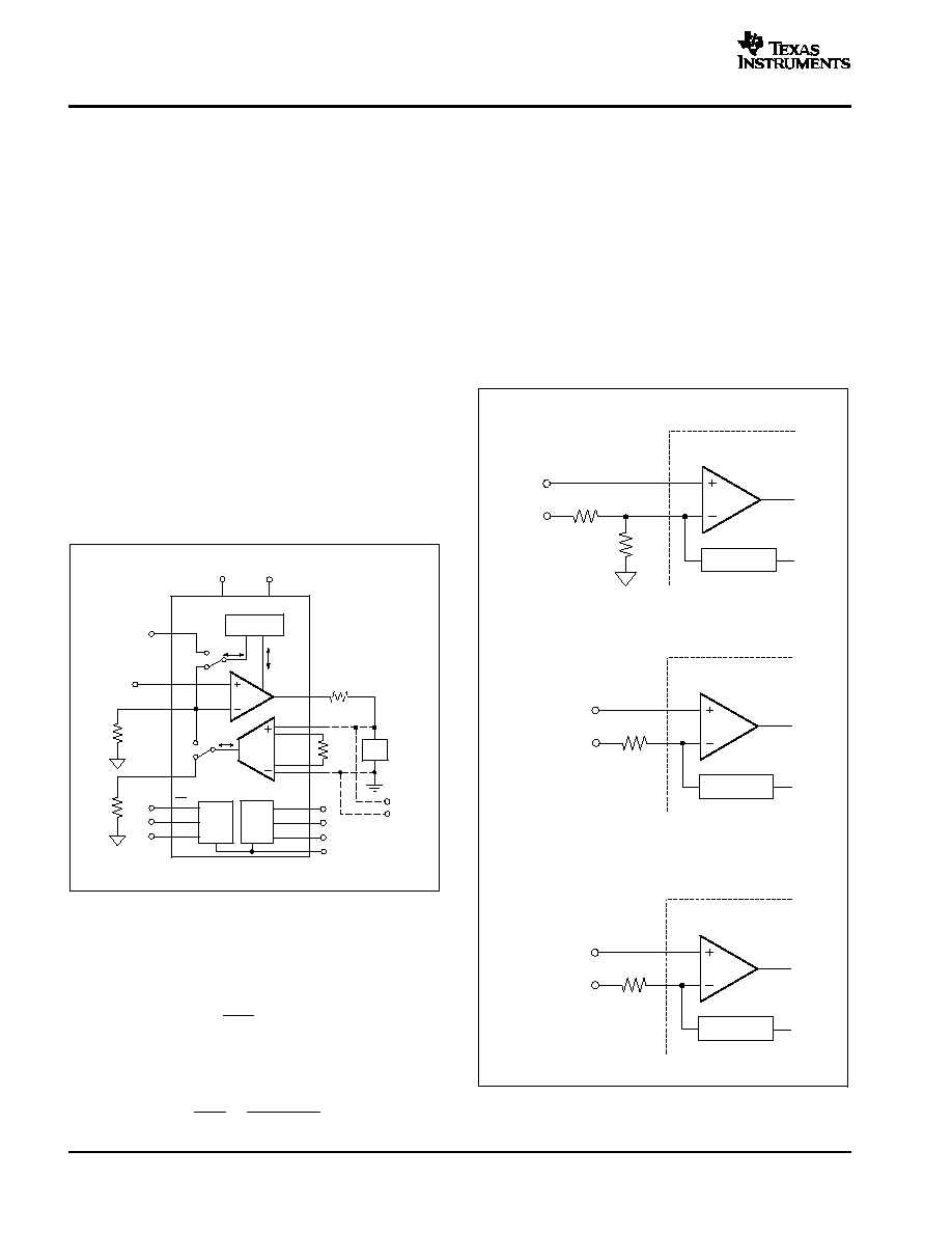
APPLICATION INFORMATION
Figure 5. Standard Circuit Configuration
D
Recommended bypassing: 100nF or more for
supply bypassing at each supply.
D
R
IMON
can be in the k
-range or short-circuited if not
used. Do not leave this current output
unconnected--it would saturate the internal current
source. The current at this I
MON
output is I
DRV
/10.
Therefore, V
IMON
= R
IMON
(I
DRV
/10).
D
R
3
is not required but can match R
SET
(or R
SET
||R
OS
)
to compensate for the bias current.
D
R
IA
can be short-circuited if not used. Do not leave
this current output unconnected. R
GAIN
is selected to
10k
to match the output of 10V with 20mA for the
equal input signal.
D
R
C
ensures stability for unknown load conditions
and limits the current into the internal protection
diodes. C
4
helps protect the device. Over-voltage
clamp diodes (standard 1N4002) might be
necessary to protect the output.
D
R
6
, R
7
, and C
5
protect the IA.
D
R
LOAD
and C
LOAD
represent the load resistance and
load capacitance.
D
R
SET
defines the transfer gain. It can be split to allow
a signal offset and, therefore, allow a 5V single-
supply digital-to-analog converter (DAC) to control a
±
10V or
±
20mA output signal.
The XTR300 can be used with asymmetric supply voltages;
however, the minimum negative supply voltage should be
equal to or more negative than -3V (typically -5V). This sup-
ply value ensures proper control of 0V and 0mA with wire re-
sistance, ground offsets, and noise added to the output. For
positive output signals, the current requirement from this
negative voltage source is less than 5mA.
GND1 through GND4 must be selected to fulfill speci-
fied operating ranges. DGND must be in the range of
(V-)
DGND
(V+) -7V.
The following information should be considered during XTR300 circuit configuration:
S-IN
IA-O
SG
OS
I-MON
IA
Current Copy
OPA
R
GAIN
10k
RG
1
RG
2
I
COPY
I
DRV
I
IA
IA
IN+
IA
IN
-
DRV
IA
OUT
V
IN
C
C
47nF
C
2
100nF
C
3
100nF
R
3
1k
R
IA
1k
NOTE: (1) See the Electrical Characteristics and Digital Input and Output section for operating limits of DGND.
(2) Connect thermal pad to V
-
.
R
OS
2k
SET
I
MON
V
-
Thermal
Pad
DGND
(1)
(2)
V+
V
-
GND
V+
XTR300
Digital
Control
OD
M2
M1
Error
Flags
EF
CM
EF
LD
EF
OT
R
SET
GND1
GND3
GND4
R
IMON
1k
R
C
15
C
4
100nF
C
5
10nF
C
LOAD
External Load
Logic Supply
(+2.7V to +5V)
Pull-up Resistors
(10k
)
R
LOAD
R
6
2.2k
R
7
2.2k
GND1
GND1
GND2

XTR300
SBOS336B - JUNE 2005 - REVISED MARCH 2006
www.ti.com
15
Built on a robust high-voltage BI-CMOS process, the
XTR300 is designed to interface the 5V or 3V supply do-
main used for processors, signal converters, and amplifi-
ers to the high-voltage and high-current industrial signal
environment. It is specified for up to
±
20V supply, but can
also be powered asymmetrically (for example, +24V and
-5V). It is designed to allow insertion of external circuit
protection elements and drive large capacitive loads.
FUNCTIONAL FEATURES
The XTR300 provides two basic functional blocks: an in-
strumentation amplifier (IA) and a driver that is a unique
operational amplifier (OPA) for current or voltage output.
This combination represents an analog output stage which
can be digitally configured to provide either current or volt-
age output to the same terminal pin. Alternatively, it can be
configured for independent measurment channels.
Three open collector error signals are provided to indicate
output related errors such as over-current or open-load
(EF
LD
) or exceeding the common-mode input range at the
IA inputs (EF
CM
). An over-temperature flag (EF
OT
) can be
used to control output disable to protect the circuit. The
monitor outputs (I
MON
and IA
OUT
) and the error flags offer
optimal testability during operation and configuration. The
I
MON
output represents the current flowing into the load in
voltage output mode, while the IA
OUT
represents the volt-
age across the connectors in current output mode. Both
monitor outputs can be connected together when used in
current or voltage output mode because the monitor sig-
nals are multiplexed accordingly.
VOLTAGE OUTPUT MODE
In voltage output mode (M1 and M2 are connected low or
left unconnected), the feedback loop through the IA pro-
vides high impedance remote sensing of the voltage at the
destination, compensating the resistance of a protection
circuit, switches, wiring, and connector resistance. The
output of the IA is a current that is proportional to the input
voltage. This current is internally routed to the OPA sum-
ming junction through a multiplexer, as shown in Figure 6.
A 1:10 copy of the output current of the OPA can be moni-
tored at the I
MON
pin. This output current and the known
output voltage can be used to calculate the load resistance
or load power.
During an output short-circuit or an over-current condition
the XTR300 output current is limited and EF
LD
(load error,
active low) flag is activated.
IA
Current Copy
OPA
R
GAIN
RG
1
RG
2
I
COPY
C
C
I
DRV
I
IA
IA
IN+
IA
IN
-
Load
GN D2
DRV
IA
OUT
V
IN
SET
I
MON
V
-
DGND
V +
XTR300
Digital
Control
OD
M2
M1
L
L
Error
Flags
EF
CM
EF
LD
EF
OT
Input Signal
R
SET
R
IMON
GND1
GND 3
Figure 6. Simplified Voltage Output Mode
Configuration
Applications not requiring the remote sense feature can
use the OPA in stand-alone operation (M1 = high). In this
case, the IA is available as a separate input channel.
The IA gain can be set by two resistors, R
GAIN
and R
SET
:
V
OUT
+
R
GAIN
2R
SET
V
IN
or when adding an offset, V
REF
, to get bidirectional output
with a single-ended input:
V
OUT
+
R
GAIN
2
V
IN
R
SET
)
V
IN
*
V
REF
R
OS
The R
SET
resistor is also used in current output mode.
Therefore, it is useful to define R
SET
for the current mode,
then set the ratio between current and voltage span with
R
GAIN
.
(1)
(2)
XTR300
SBOS336B - JUNE 2005 - REVISED MARCH 2006
www.ti.com
16
CURRENT OUTPUT MODE
The XTR300 does not require a shunt resistor for current
control because it uses a precise current mirror arrange-
ment.
In current output mode (M1 connected low, or left uncon-
nected and M2 connected high) a precise copy of 1/10th
of the output is internally routed back to the summing junc-
tion of the OPA through a multiplexer, closing the control
loop for the output current.
The OPA driver can deliver more than
±
24mA within a wide
output voltage range. An open-output condition or high-im-
pedance load that prevents the flow of the required current
activates the EF
LD
flag.
While in current output mode, a current (I
IA
) that is propor-
tional to the voltage at the IA input is routed to IA
OUT
and
can be used to monitor the load voltage. A resistor con-
verts this current into voltage. This arrangement makes
level shifting easy.
Alternatively, the IA can be used as an independent moni-
toring channel. If this output is not used, connect it to GND
to maintain proper function of the monitor stage, as shown
in Figure 7.
IA
Current Copy
OPA
R
GAIN
RG
1
RG
2
I
COPY
I
DRV
I
IA
IA
IN+
IA
IN
-
Load
GND2
DRV
IA
OUT
V
IN
SET
I
MON
V
-
DGND
V+
XTR300
Digital
Control
OD
M2
M1
H
L
Error
Flags
EF
CM
EF
LD
EF
OT
Input Signal
R
IA
R
SET
GND3
GND1
Figure 7. Simplified Current Output Mode
Configuration
The transconductance (gain) can be set by the resistor,
R
SET
, according to the equation:
I
OUT
+
10
R
SET
V
IN
or when adding an offset V
REF
to get bidirectional output
with a single-ended input:
I
OUT
+
10
V
IN
R
SET
)
V
IN
*
V
REF
R
OS
INPUT SIGNAL CONNECTION
It is possible to drive the XTR300 with a unidirectional input
signal and still get a bidirectional output by adding an addi-
tional resistor, R
OS
, and an offset voltage signal, V
REF
. It
can be a mid-point voltage or a signal to shift the output
voltage to a desired value.
This design is illustrated in Figure 8a, Figure 8b, and
Figure 8c. As with a normal operational amplifier, there are
several options for offset-shift circuits. The input can be
connected for inverting or noninverting gain. Unlike many
op amp input circuits, however, this configuration uses cur-
rent feedback, which removes the voltage relationship be-
tween the noninverting input and output potential because
there is no feedback resistor.
V
IN
(
±
V
MIDSCALE
)
V
MIDSCALE
R
SET
1k
XTR300
OPA
I-Feedback
V
IN
(
±
V
OFFSET
)
V
REF
R
SET
1k
XTR300
OPA
I-Feedback
a) Noninverting Input
b) Noninverting Input
c) Inverting Input (V
REF
= V
OFFSET
)
V
IN
(0 to V
OFFSET
)
V
REF
R
OS
2k
R
SET
2k
XTR300
OPA
I-Feedback
Figure 8. Circuit Options for Op Amp Output
Level-Shifting
(3)
(4)

XTR300
SBOS336B - JUNE 2005 - REVISED MARCH 2006
www.ti.com
17
The input bias current effect on the offset voltage can be
reduced by connecting a resistor in series with the positive
input that matches the approximate resistance at the neg-
ative input. This resistor placed close to the input pin acts
as a damping element and makes the design less sensitive
to RF noise. See R
3
in Figure 5.
EXTERNALLY-CONFIGURED MODE:
OPA AND IA
It is possible to use the precision of the operational amplifi-
er (OPA) and instrumentation amplifier (IA) independently
from each other by configuring the digital control pins (M1
high). In this mode, the IA output current is routed to IA
OUT
and the copy of the OPA output current is routed to I
MON
,
as shown in Figure 4.
This mode allows external configuration of the analog sig-
nal routing and feedback loop.
The current output IA has high input impedance, low offset
voltage and drift, and very high common-mode rejection
ratio. An external resistor (R
IA
) can be used to convert the
output current of the IA (I
IA
) to an output voltage. The gain
is given by:
I
IA
+
2
R
GAIN
V
IN
or V
IA
+
2R
IA
R
GAIN
V
IN
The OPA provides low drift and high voltage output swing
that can be used like a common operational amplifier by
connecting a feedback network around it. In this mode, the
copy of the output current is available at the I
MON
pin (it in-
cludes the current into the feedback network). It provides
an output current limit for protection, which can be set be-
tween two ranges by M2. The error flag indicates an over-
current condition, as well as indicating driving the output
into the supply rails.
Alternatively, the feedback can be closed through the I
MON
pin to create a precise voltage-to-current converter.
DRIVER OUTPUT DISABLE
The OPA output (DRV) can be switched to a high-imped-
ance mode by driving the OD control pin low. This input can
be connected to the over-temperature flag, EF
OT
, and a
pull-up resistor to protect the IC from over-temperature by
disconnecting the load.
The output disable mode can be used to sense and mea-
sure the voltage at the IA input pins without loading from
the DRV output. This mode allows testing of any voltage
present at the I/O connector. However, consider the bias
current of the IA input pins.
The digital control inputs, M1 and M2, set the four opera-
tion modes of the XTR300 as shown in Table 1. When M1
is asserted low, M2 determines voltage or current mode
and the corresponding appropriate current limit (I
SC
) set-
ting. When M1 is high, the internal feedback connections
are opened; IA
OUT
and I
MON
are both connected to the out-
put pins; and M2 only determines the current limit (I
SC
) set-
ting.
SUMMARY OF CONFIGURATION MODES
(1)
M1
M2
MODE
DESCRIPTION
L
L
V
OUT
Voltage Output Mode, I
SC
= 20mA
L
H
I
OUT
Current Output Mode, I
SC
= 32mA
H
L
Ext
IA and I
MON
on ext. pins, I
SC
= 20mA
H
H
Ext
IA and I
MON
on ext. pins, I
SC
= 32mA
(1) OD is a control pin independent of M1 or M2. See the Driver
Output Disable section.
Table 1. Mode Configuration
M1 and M2 are pulled low internally with 1
µ
A. Terminate
these two pins to avoid noise coupling.
Output disable (OD) is internally pulled high with approxi-
mately 1
µ
A.
DRIVING CAPACITIVE LOADS AND LOOP
COMPENSATION
For normal operation, the driver OPA and the IA are con-
nected in a closed loop for voltage output. In current output
mode, the current copy closes the loop directly.
In current output mode, loop compensation is not critical,
even for large capacitive loads. However, in voltage output
mode, the capacitive load, together with the source imped-
ance and the impedance of the protection circuit, gener-
ates additional phase lag. The IA input might also be pro-
tected by a low-pass filter that influences phase in the
closed loop.
The loop compensation low-pass filter consists of C
C
and
the parallel resistance of R
OS
and R
SET
. For loop stability
with large capacitive load, the external phase shift has to
be added to the OPA phase. With C
C
, the voltage gain of
the OPA has to approach zero at the frequency where the
total phase approaches 180
∞
+ 135
∞
.
The best stability for large capacitive loads is provided by
adding a small resistor, R
C
(15
). See the Output Protec-
tion section.
An empirical method of evaluation is using a square wave
input signal and observing the settling after transients. Use
small signal amplitudes only--steep signal edges cause
excessive current to flow into the capacitive load and may
activate the current limit, which hides or prevents oscilla-
tion. A small-signal oscillation can be hidden from large ca-
pacitive loads, but observing the I
MON
output on an ap-
propriate resistor (use a similar value like R
SET
||R
OS
) would
indicate stability issues. Note that noise pulses at I
MON
dur-
(5)

XTR300
SBOS336B - JUNE 2005 - REVISED MARCH 2006
www.ti.com
18
ing overload (EF
LD
active) are normal and are caused by
cycling of the current mirror.
The voltage output mode includes the IA in the loop. An
additional low-pass filter in the input reverses the phase
and therefore increases the signal bandwidth of the loop,
but also increases the delay. Again, loop stability has to be
observed. Overloading the IA disconnects the closed loop
and the output voltage rails.
INTERNAL CURRENT SOURCES,
SWITCHING NOISE, AND SETTLING TIME
The accuracy of the current output mode and the DC per-
formance of the IA rely on dynamically-matched current
mirrors.
Identical current sources are rotated to average out mis-
match errors. It can take several clock cycles of the internal
100kHz ocsillator (or a submultiple of that frequency) to
reach full accuracy. This may dominate the settling time to
the 0.1% accuracy level and can be as much as 100
µ
s in
current output mode or 40
µ
s in voltage output mode.
A small portion of the switching glitches appear at the DRV
output, and also at the I
MON
and IA
MON
outputs. The stan-
dard circuit configuration, with R
C
, C
4
, and C
C
, which are
required for loop compensation and output protection, also
helps reduce the noise to negligible levels at the signal out-
put. If necessary, the monitor outputs can be filtered with
a shunt capacitor.
IA STRUCTURE, VOLTAGE MONITOR
The instrumentation amplifier has high-impedance NPN
transistor inputs that do not load the output signal, which
is especially important in current output mode. The output
signal is a controlled current that is multiplexed either to
the SET pin (to close the voltage output loop) or to IA
OUT
(for external access).
The principal circuit is shown in Figure 9. The two input
buffer amplifiers reproduce the input difference voltage
across R
GAIN
. The resulting current through this resistor is
bidirectionally mirrored to the output. That mirroring results
in the ideal transfer function of:
I
IA
+
IA
OUT
+
2 (IA
IN
)
*
IA
IN
*
) R
GAIN
The accuracy and drift of R
GAIN
defines the accuracy of the
voltage to current conversion. The high accuracy and sta-
bility of the current mirrors result from a cycling chopper
technique.
Current Mirror
Current Mirror
Current Mirror
Current Mirror
IA
IN+
IA
IN
-
R
GAIN
I
R
I
R
I
R
I
R
2I
R
2I
R
2I
R
2I
R
A1
A2
I
IA
Figure 9. IA Block Diagram
The output current, IA
OUT
, of the instrumentation amplifier
is limited to protect the internal circuitry. This current limit
has two settings controlled by the state of M2 (see Electri-
cal Characteristics, Short-Circuit Current specification).
Note that if R
SET
is too small, the current output limitation
of the instrumentation amplifier can disrupt the closed loop
of the XTR300 in voltage output mode. With M2 = low, the
nominal R
GAIN
of 10k
allows an input voltage of 20V
PP
,
which produces an output current of 4mA
PP
. When using
lower resistors for R
GAIN
that can allow higher currents, the
IA output current limitation must be taken into account.
CURRENT MONITOR
In current output mode (M2 = high), the XTR300 provides
high output impedance. A precision current mirror gener-
ates an exact 1/10th copy of the output current and this cur-
rent is either routed to the summing junction of the OPA to
close the feedback loop (in the current output mode) or to
the I
MON
pin for output current monitoring in other operating
modes.
(6)

XTR300
SBOS336B - JUNE 2005 - REVISED MARCH 2006
www.ti.com
19
The high accuracy and stability of this current split results
from a cycling chopper technique. This design eliminates
the need for a precise shunt resistor or a precise shunt-
voltage measurement, which would require high common-
mode rejection performance.
During a saturation condition of the DRV output (the error
flag is active), the monitor output (I
MON
) shows a current
peak because the loop opens. Glitches from the current
mirror chopper appear during this time in the monitor sig-
nal. This part of the signal cannot be used for measure-
ment.
ERROR FLAGS
The XTR300 is designed for testability of its proper func-
tion and allows observation of the conditions at the load
connection without disrupting service.
If the output signal is not in accordance to the transfer func-
tion, an error flag is activated (limited by the dynamic re-
sponse capabilities). These error flags are in addition to
the monitor outputs, I
MON
and IA
OUT
, which allow the mo-
mentary output current (in voltage mode) or output voltage
(in current mode) to be read back.
This combination of error flag and monitor signal allows
easy observation of the XTR300 for function and working
condition, providing the basis for not only remote control,
but also for remote diagnosis.
All error flags of the XTR300 have open collector outputs
with a weak pull-up of approximately 1
µ
A to an internal 5V.
External pull-up resistors to the logic voltage are required
when driving 3V or 5V logic.
The output sink current should not exceed 5mA. This is just
enough to directly drive optical-couplers, but a current-lim-
iting resistor is required.
There are three error flags:
D
IA Common-Mode Over-Range (EF
CM
)--goes low
as soon as the inputs of the IA reach the limits of the
linear operation for the input voltage.
This flag shows noise from the saturated current
mirrors which can be filtered with a capacitor to GND.
D
Load Error (EF
LD
)--indicates fault conditions driving
voltage or current into the load. In voltage output mode
it monitors the voltage limits of the output swing and
the current limit condition caused from short or low
load resistance. In current output mode it indicates a
saturation into the supply rails from a high load
resistance or open load.
D
Over-Temperature Flag (EF
OT
)--is a digital output
that goes low if the chip temperature reaches a
temperature of +140
∞
C and resets as soon as it cools
down to +125
∞
C. It does not automatically shut down
the output; it allows the user system to take action on
the situation. If desired, this output can be connected
to output disable (OD) which disables the output and
therefore removes the source of power. This
connection acts like an automatic shut down, but
requires an external pull-up resistor to safely override
the internal current sources. The IA channel is not
affected, which allows continuous observation of the
voltage at the output.
DIGITAL COMMUNICATION: HART
The bandwidth and drive capability of the XTR300 are
sufficient to transmit communication signals such as
HART. The combination of current monitor and voltage
sense with the IA circuit enables communication signal
transmission from the signal output connector to the
monitor pins in both current or voltage output mode. In
current output mode, the signal arrives at IA
OUT
; in voltage
output mode the communication signal modulates the
DRV current and arrives at I
MON
. Both IA
OUT
and I
MON
can
be connected together because they are internally
multiplexed according to the output mode (while M1 = low).
Driving a communication signal through the output
connector back into the system or sensor, regardless of
the output mode, enables easy configuration, calibration,
diagnosis, and universal communication.
DIGITAL I/O AND GROUND
CONSIDERATIONS
The XTR300 offers voltage output mode, current output
mode, external configuration, and instrumentation mode
(voltage input). In addition, the internal feedback mode can
be disconnected and external loop connections can be
made. These modes are controlled by M1 and M2 (see the
function table). The OD input pin controls enable or disable
of the output stage (OD is active low).
The digital I/O is referenced to DGND and signals on this
pin should remain within 5V of the DGND potential. This
DGND pin carries the output low-current (sink current) of
the logic outputs. DGND can be connected to a potential
within the supply voltage but needs to be 8V below the
positive supply. Proper connection avoids current from the
digital outputs flowing into the analog ground.
It is important to note that DGND has normally reverse-
biased diodes connected to the supply. Therefore, high
and destructive currents could flow if DGND is driven
beyond the supply rails by more than a diode forward
voltage. Avoid this condition during power-on and
power-off!

XTR300
SBOS336B - JUNE 2005 - REVISED MARCH 2006
www.ti.com
20
OUTPUT PROTECTION
The XTR300 is intended to operate in a harsh industrial
environment. Therefore, a robust semiconductor process
was chosen for this design. However, some external
protection is still required.
The instrumentation amplifier inputs can be protected by
external resistors that limit current into the protection cell
behind the IC-pins, as shown in Figure 10. This cell
conducts to the power-supply connection through a diode
as soon as the input voltage exceeds the supply voltage.
The circuit configuration example shows how to arrange
these two external resistors.
The bias current is best cancelled if both resistors are
equal. The additional capacitor reduces RF noise in the
input signal to the IA.
RG
1
RG
2
IA
IN+
IA
IN+
R
GAIN
R
6
2.2k
R
7
2.2k
C
5
10nF
V
SENSE+
V
SENSE
-
IA
Figure 10. Current Limiting Resistors
The load connection to the DRV output must be low
impedance; therefore, external protection diodes may be
necessary to handle excessive currents, as shown in
Figure 11. The internal protection diodes start to conduct
earlier than a normal external PN-type diode because they
are affected by the higher die temperature. Therefore,
either Schottky diodes are required, or an additional
resistor (R
C
) can be placed in series with the input. An
example of this protection is shown in Figure 11. Assuming
the standard diodes limit the voltage to 1.4V and the
internal diodes clamp at 0.7V, this resistor can limit the
current into the internal protection diodes to 50mA:
(1.4V
*
0.7V) 15
W +
47mA
R
C
is also part of the recommended loop compensation. C
4
helps protect the output against RFI and high-voltage
spikes.
OPA
XTR300
I/V OUT
V+
V
-
C
C
47nF
R
C
15
C
4
100nF
D
1N4002
D
1N4002
DRV
Figure 11. Example for DRV Output Protection
POWER ON/OFF GLITCH
When power is turned on or off, most analog amplifiers
generate some glitching of the output because of internal
circuit thresholds and capacitive charges. Characteristics
of the supply voltage, as well as its rise and fall time, also
directly influence output glitches. Load resistance and
capacitive load affect the amplitude as well.
The output disable control (OD) allows good control over
the output during power-on, power-off, and system down
time by providing a high impedance to the output.
Figure 12a, Figure 12b, and Figure 12c show the output
voltage with the output disabled during power on and
off--no glitch can be see on the output signal. Holding OD
low also prevents glitches in current output mode.
Figure 12c indicates no glitches when transitioning from
disable to enable.
All measurements are made with a load resistance of 1k
and tested in the circuit configuration of Figure 5. OD has
an internal pull-up of approximately 1
µ
A; therefore, a
100k
resistor provides safe pull-down during power
on--make sure the logic controlling the OD pin does not
glitch.
(7)

XTR300
SBOS336B - JUNE 2005 - REVISED MARCH 2006
www.ti.com
21
a) Power-on in voltage or current output mode.
CH 1 shows supply voltage; CH 2 output voltage across a 1k
load.
b) Power-off in voltage or current output mode.
CH 1 shows supply voltage; CH 2 output voltage across a 1k
load.
Power-Supply Voltage
5.0V/div
Output
0.5V/div
Time (10ms/div)
Power-Supply Voltage
5.0V/div
Output
0.5V/div
Time (10ms/div)
Time (10ms/div)
OD
2.0V/div
Output
0.5V/div
c) CH 2: Output signal during toggle of OD:
CH 1 voltage or current output mode across a 1k
load.
Figure 12. Output Signal with Output Disabled During Power On/Off
LAYOUT CONSIDERATIONS
Supply bypass capacitors should be close to the package
and connected with low-impedance conductors. Avoid
noise coupled into R
GAIN
, and observe wiring resistance.
For thermal management, see the Heat Sinking section.
Layout for the XTR300 is not critical; however, its internal
current chopping works best with good (low dynamic
impedance) supply decoupling. Therefore, avoid through-
hole contacts in the connection to the bypass capacitors
or use multiple through-hole contacts. Switching noise
from chopper-type power supplies should be filtered
enough to reduce influence on the circuit. Small resistors
(2
, for example) or damping inductors in series with the
supply connection (between the DC/DC converter and the
XTR circuit) act as a decoupling filter together with the
bypass capacitor, as shown in Figure 13.
V
-
V+
V
-
V+
C
B1
100nF
C
B3
1
µ
F
C
B4
1
µ
F
C
B2
100nF
L
1
10
µ
H
L
2
10
µ
H
XTR300
Figure 13. Suggested Supply Decoupling for
Noisy Chopper-Type Supplies

XTR300
SBOS336B - JUNE 2005 - REVISED MARCH 2006
www.ti.com
22
Resistors connected close to the input pins help dampen
environmental noise coupled into conductor traces.
Therefore, place the OPA input- and IA input-related
resistors close to the package. Also, avoid additional wire
resistance in series to R
SET
, R
OS
, and R
GAIN
(observe the
reliability of the through-hole contacts), because this could
produce gain and offset error as well as drift; 1
is already
0.1% of the 1k
resistor.
The exposed lead-frame die pad on the bottom of the
package must be connected to V-, pin 11 (see the QFN
Package section for more details).
QFN PACKAGE
The XTR300 is available in a QFN package. This leadless,
near chip-scale package maximizes board space and
enhances thermal and electrical characteristics through
an exposed pad.
QFN packages are physically small, have a smaller
routing area, and improved thermal performance. For
optimal heat performance, the exposed power pad must
be connected to an adequate heat slug with at least six
thermal vias to a copper area. See the example land
pattern RGW (S-PQFP-N20), available for download at
www.ti.com or at the end of this datasheet.
The QFN package can be easily mounted using standard
printed circuit board (PCB) assembly techniques. See
Application Note, QFN/SON PCB Attachment (SLUA271)
and Application Report, Quad Flatpack No-Lead Logic
Packages (SCBA017), available for download at
www.ti.com, for more information.
The exposed leadframe die pad on the bottom of the
package must be connected to the V- pin, and proper heat
sinking has to be provided.
HEAT SINKING
Power dissipation depends on power supply, signal, and
load conditions. It is dominated by the power dissipation of
the output transistors of the OPA. For DC signals, power
dissipation is equal to the product of output current, I
OUT
and the output voltage across the conducting output
transistor (V
S
- V
OUT
).
It is important to note that the temperature protection will
not shut the part down in over-temperature conditions,
unless the EF
OT
pin is connected to the output enable pin
OD; see the section on Driver Output Disable.
The power that can be safely dissipated by the package is
related to the ambient temperature and the heatsink
design.
The QFN package was specifically designed to provide
excellent power dissipation, but board layout greatly
influences the heat dissipation of the package. Refer to the
QFN Package section for further details.
The XTR300 has a junction-to-ambient thermal resistance
(
q
JA
) value of 38
∞
C/W when soldered to a 2-oz copper
plane. This value can be further decreased by the addition
of forced air. See Table 2 for the junction-to-ambient
thermal resistance of the QFN-20 package. Junction
temperature should be kept below +125
∞
C for reliable
operation. The junction temperature can be calculated by:
T
J
= T
A
+ P
D
∑
q
JA
where
q
JA
=
q
JC
+
q
CA
T
J
= Junction Temperature (
∞
C)
T
A
= Ambient Temperature (
∞
C)
PD = Power Dissipated (W)
q
JA
= Junction-to-Ambient Thermal Resistance
q
JC
= Junction-to-Case Thermal Resistance
q
CA
= Case-to-Air Thermal Resistance
HEATSINKING METHOD
q
JA
The part is soldered to a 2-oz copper pad under the
exposed pad.
38
Soldered to copper pad with forced airflow (150lfm).
36
Soldered to copper pad with forced airflow (250lfm).
35
Soldered to copper pad with forced airflow (500lfm).
34
Table 2. Junction-to-Ambient Thermal Resistance
with Various Heatsinking Efforts
To appropriately determine the required heatsink area,
required power dissipation should be calculated and the
relationship between power dissipation and thermal
resistance should be considered to minimize overheat
conditions and allow for reliable long-term operation.
The efficiency of the heat sinking can be tested using the
EF
OT
output signal. This output goes low at nominally
+140
∞
C junction temperature (assume 6% tolerance).
With full-power dissipation--for example, maximum
current into a 0
load--the ambient temperature can be
slowly raised until the OT flag goes low; at this point, the
usable operation condition is determined.
The recommended landing pattern is shown in document
RGW (S-PQFP-N20). The nine (not less than six) through-
hole contacts of the inner heat sink solder pad connect to
a copper plane in any one layer. It must be large enough
to efficiently distribute the heat into the PCB. This pad has
to be electrically connected to the V- pin to provide the
required substrate connection.

PACKAGING INFORMATION
Orderable Device
Status
(1)
Package
Type
Package
Drawing
Pins Package
Qty
Eco Plan
(2)
Lead/Ball Finish
MSL Peak Temp
(3)
XTR300AIRGWR
ACTIVE
QFN
RGW
20
3000 Green (RoHS &
no Sb/Br)
CU NIPDAU
Level-2-260C-1 YEAR
XTR300AIRGWRG4
ACTIVE
QFN
RGW
20
3000 Green (RoHS &
no Sb/Br)
CU NIPDAU
Level-2-260C-1 YEAR
XTR300AIRGWT
ACTIVE
QFN
RGW
20
250
Green (RoHS &
no Sb/Br)
CU NIPDAU
Level-2-260C-1 YEAR
XTR300AIRGWTG4
ACTIVE
QFN
RGW
20
250
Green (RoHS &
no Sb/Br)
CU NIPDAU
Level-2-260C-1 YEAR
(1)
The marketing status values are defined as follows:
ACTIVE: Product device recommended for new designs.
LIFEBUY: TI has announced that the device will be discontinued, and a lifetime-buy period is in effect.
NRND: Not recommended for new designs. Device is in production to support existing customers, but TI does not recommend using this part in
a new design.
PREVIEW: Device has been announced but is not in production. Samples may or may not be available.
OBSOLETE: TI has discontinued the production of the device.
(2)
Eco Plan - The planned eco-friendly classification: Pb-Free (RoHS), Pb-Free (RoHS Exempt), or Green (RoHS & no Sb/Br) - please check
http://www.ti.com/productcontent
for the latest availability information and additional product content details.
TBD: The Pb-Free/Green conversion plan has not been defined.
Pb-Free (RoHS): TI's terms "Lead-Free" or "Pb-Free" mean semiconductor products that are compatible with the current RoHS requirements
for all 6 substances, including the requirement that lead not exceed 0.1% by weight in homogeneous materials. Where designed to be soldered
at high temperatures, TI Pb-Free products are suitable for use in specified lead-free processes.
Pb-Free (RoHS Exempt): This component has a RoHS exemption for either 1) lead-based flip-chip solder bumps used between the die and
package, or 2) lead-based die adhesive used between the die and leadframe. The component is otherwise considered Pb-Free (RoHS
compatible) as defined above.
Green (RoHS & no Sb/Br): TI defines "Green" to mean Pb-Free (RoHS compatible), and free of Bromine (Br) and Antimony (Sb) based flame
retardants (Br or Sb do not exceed 0.1% by weight in homogeneous material)
(3)
MSL, Peak Temp. -- The Moisture Sensitivity Level rating according to the JEDEC industry standard classifications, and peak solder
temperature.
Important Information and Disclaimer:The information provided on this page represents TI's knowledge and belief as of the date that it is
provided. TI bases its knowledge and belief on information provided by third parties, and makes no representation or warranty as to the
accuracy of such information. Efforts are underway to better integrate information from third parties. TI has taken and continues to take
reasonable steps to provide representative and accurate information but may not have conducted destructive testing or chemical analysis on
incoming materials and chemicals. TI and TI suppliers consider certain information to be proprietary, and thus CAS numbers and other limited
information may not be available for release.
In no event shall TI's liability arising out of such information exceed the total purchase price of the TI part(s) at issue in this document sold by TI
to Customer on an annual basis.
PACKAGE OPTION ADDENDUM
www.ti.com
14-Mar-2006
Addendum-Page 1


IMPORTANT NOTICE
Texas Instruments Incorporated and its subsidiaries (TI) reserve the right to make corrections, modifications,
enhancements, improvements, and other changes to its products and services at any time and to discontinue
any product or service without notice. Customers should obtain the latest relevant information before placing
orders and should verify that such information is current and complete. All products are sold subject to TI's terms
and conditions of sale supplied at the time of order acknowledgment.
TI warrants performance of its hardware products to the specifications applicable at the time of sale in
accordance with TI's standard warranty. Testing and other quality control techniques are used to the extent TI
deems necessary to support this warranty. Except where mandated by government requirements, testing of all
parameters of each product is not necessarily performed.
TI assumes no liability for applications assistance or customer product design. Customers are responsible for
their products and applications using TI components. To minimize the risks associated with customer products
and applications, customers should provide adequate design and operating safeguards.
TI does not warrant or represent that any license, either express or implied, is granted under any TI patent right,
copyright, mask work right, or other TI intellectual property right relating to any combination, machine, or process
in which TI products or services are used. Information published by TI regarding third-party products or services
does not constitute a license from TI to use such products or services or a warranty or endorsement thereof.
Use of such information may require a license from a third party under the patents or other intellectual property
of the third party, or a license from TI under the patents or other intellectual property of TI.
Reproduction of information in TI data books or data sheets is permissible only if reproduction is without
alteration and is accompanied by all associated warranties, conditions, limitations, and notices. Reproduction
of this information with alteration is an unfair and deceptive business practice. TI is not responsible or liable for
such altered documentation.
Resale of TI products or services with statements different from or beyond the parameters stated by TI for that
product or service voids all express and any implied warranties for the associated TI product or service and
is an unfair and deceptive business practice. TI is not responsible or liable for any such statements.
Following are URLs where you can obtain information on other Texas Instruments products and application
solutions:
Products
Applications
Amplifiers
amplifier.ti.com
Audio
www.ti.com/audio
Data Converters
dataconverter.ti.com
Automotive
www.ti.com/automotive
DSP
dsp.ti.com
Broadband
www.ti.com/broadband
Interface
interface.ti.com
Digital Control
www.ti.com/digitalcontrol
Logic
logic.ti.com
Military
www.ti.com/military
Power Mgmt
power.ti.com
Optical Networking
www.ti.com/opticalnetwork
Microcontrollers
microcontroller.ti.com
Security
www.ti.com/security
Telephony
www.ti.com/telephony
Video & Imaging
www.ti.com/video
Wireless
www.ti.com/wireless
Mailing Address:
Texas Instruments
Post Office Box 655303 Dallas, Texas 75265
Copyright 2006, Texas Instruments Incorporated