N-Channel JFET
General Purpose Amplifier
2N4117 ≠ 2N4119 / 2N4117A ≠ 2N4119A
PN4117 ≠ PN4119 / PN4117A ≠ PN4119A / SST4117 ≠ SST4119
FEATURES
∑
∑
Low Leakage
∑
∑
Low Capacitance
ABSOLUTE MAXIMUM RATINGS
(T
A
= 25
o
C unless otherwise noted)
Gate-Source or Gate-Drain Voltage . . . . . . . . . . . . . . . . -40V
Gate Current . . . . . . . . . . . . . . . . . . . . . . . . . . . . . . . . . 50mA
Storage Temperature Range . . . . . . . . . . . . . -65
o
C to +200
o
C
Operating Temperature Range . . . . . . . . . . . -55
o
C to +175
o
C
Lead Temperature (Soldering, 10sec) . . . . . . . . . . . . . +300
o
C
Power Dissipation . . . . . . . . . . . . . . . . . . . . . . . . . . . . 300mW
Derate
above
25
o
C . . . . . . . . . . . . . . . . . . . . . . . 2.0mW/
o
C
NOTE: Stresses above those listed under "Absolute Maximum
Ratings" may cause permanent damage to the device. These are
stress ratings only and functional operation of the device at these or
any other conditions above those indicated in the operational sections
of the specifications is not implied. Exposure to absolute maximum
rating conditions for extended periods may affect device reliability.
ORDERING INFORMATION
Part
Package
Temperature Range
2N4117-19/A Hermetic TO-72
-55
o
C to +175
o
C
PN4117-19/A Plastic TO-92
-55
o
C to +135
o
C
SST4117-19
Plastic SOT-23
-55
o
C to +135
o
C
X2N4117-19/A Sorted Chips in Carriers
-55
o
C to +175
o
C
CORPORATION
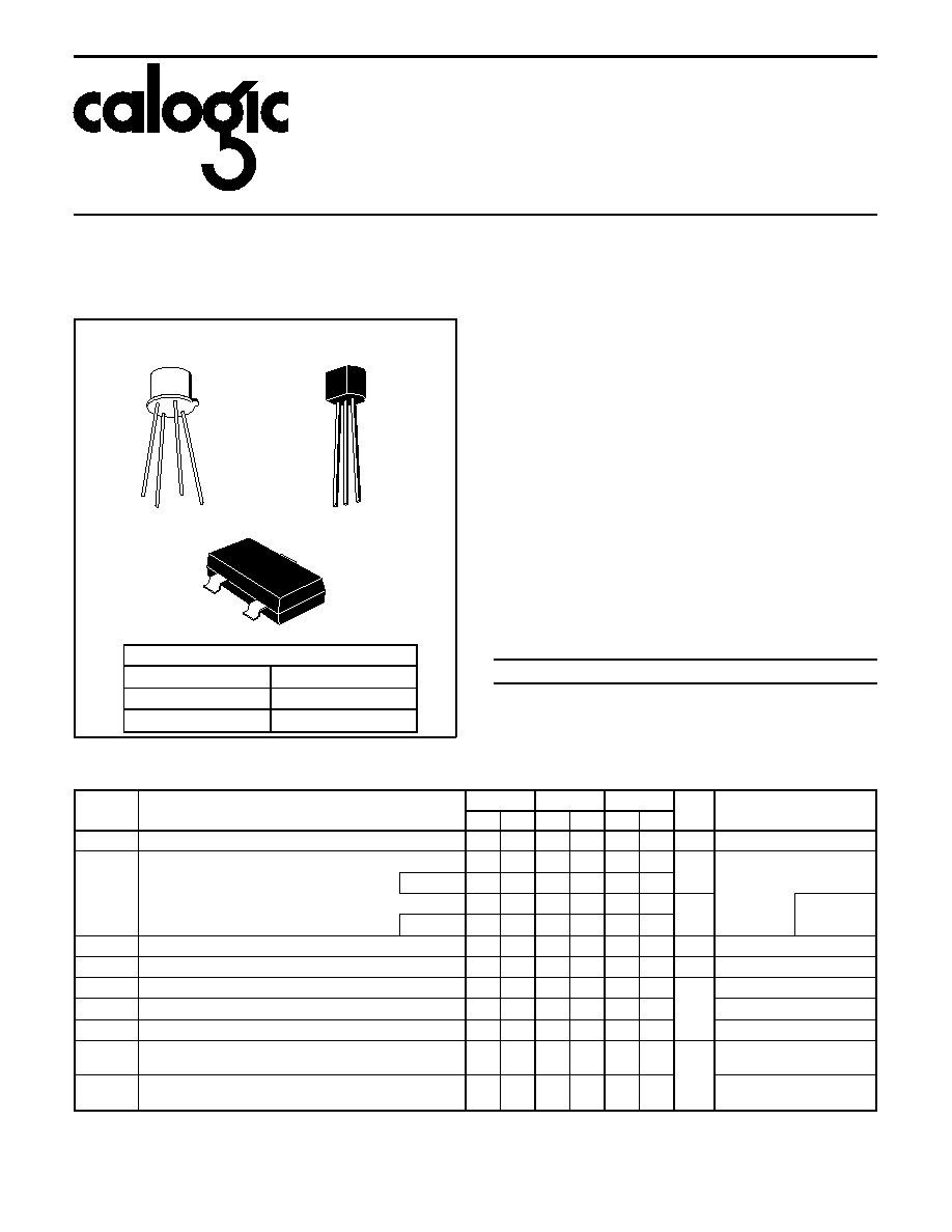
PIN CONFIGURATION
TO-72
G
D
C
S
ELECTRICAL CHARACTERISTICS (T
A
= 25
o
C unless otherwise specified)
SYMBOL
PARAMETER
4117/A
4118/A
4119/A
UNITS
TEST CONDITIONS
MIN MAX MIN MAX MIN MAX
BV
GSS
Gate-Source Breakdown Voltage
-40
-40
-40
V
I
G
= -1
µ
A, V
DS
= 0
I
GSS
Gate Reverse Current
-10
-10
-10
pA
A devices
-1
-1
-1
V
GS
= -20V, V
DS
= 0
-25
-25
-25
nA
T
A
= +150
o
C
A devices
-2.5
-2.5
-2.5
V
GS(off)
Gate-Source Pinch-Off Voltage
-0.6
-1.8
-1
-3
-2
-6
V
V
DS
= 10V, I
D
= 1nA
I
DSS
Drain Current at Zero Gate Voltage (Note 1)
0.02 0.09 0.08 0.24 0.20 0.60
mA
V
DS
= 10V, V
GS
= 0
g
fs
Common-Source Forward Transconductance (Note 1)
70
210
80
250
100
330
µ
S
V
DS
= 10V, f = 1kHz
g
fs
Common-Source Forward Transconductance (Note 2)
60
70
90
V
GS
= 0, f = 30MHz
g
os
Common-Source Output Conductance
3
5
10
V
DS
= 10V, V
GS
= 0, f = 1kHz
C
iss
Common-Source Input Capacitance (Note 2)
3
3
3
pF
V
DS
= 10V, V
GS
= 0,
f = 1MHz
C
rss
Common-Source Reverse Transfer Capacitance (Note 2)
1.5
1.5
1.5
V
DS
= 10V, V
GS
= 0,
f = 1MHz
NOTES: 1. Pulse test: Pulse duration of 2ms used during test.
2. For design reference only, not 100% tested.
D S
G
T O - 92
SOT-23
G
S
D
PRODUCT MARKING (SOT-23)
SST4117
T17
SST4118
T18
SST4119
T19
5007