N-Channel JFET Switch
2N5434
FEATURES
∑
∑
Low r
ds(on)
∑
∑
Excellent Switching
∑
∑
Low Cutoff Current
ABSOLUTE MAXIMUM RATINGS
(T
A
= 25
o
C unless otherwise noted)
Gate-Source Voltage . . . . . . . . . . . . . . . . . . . . . . . . . . . . -25V
Gate-Drain Voltage . . . . . . . . . . . . . . . . . . . . . . . . . . . . . -25V
Gate Current . . . . . . . . . . . . . . . . . . . . . . . . . . . . . . . . 100mA
Drain Current . . . . . . . . . . . . . . . . . . . . . . . . . . . . . . . . 400mA
Storage Temperature Range . . . . . . . . . . . . . -65
o
C to +200
o
C
Operating Temperature Range . . . . . . . . . . . -55
o
C to +150
o
C
Lead Temperature (Soldering, 10sec) . . . . . . . . . . . . . +300
o
C
Power Dissipation . . . . . . . . . . . . . . . . . . . . . . . . . . . . 300mW
Derate
above
25
o
C . . . . . . . . . . . . . . . . . . . . . . . 2.3mW/
o
C
NOTE: Stresses above those listed under "Absolute Maximum
Ratings" may cause permanent damage to the device. These are
stress ratings only and functional operation of the device at these or
any other conditions above those indicated in the operational sections
of the specifications is not implied. Exposure to absolute maximum
rating conditions for extended periods may affect device reliability.
ORDERING INFORMATION
Part
Package
Temperature Range
2N5434
Hermetic TO-52
-55
o
C to +150
o
C
X2N5434
Sorted Chips in Carriers
-55
o
C to +150
o
C
CORPORATION
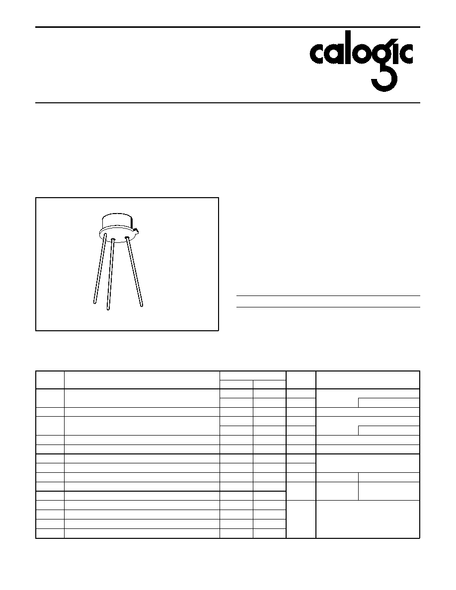
PIN CONFIGURATION
D
S
(TO-52)
G, C
ELECTRICAL CHARACTERISTICS (T
A
= 25
o
C unless otherwise specified)
SYMBOL
PARAMETER
2N5434
UNITS
TEST CONDITIONS
MIN
MAX
I
GSS
Gate Reverse Current
-200
pA
V
GS
= -15V, V
DS
= 0
-200
nA
T
A
= 150
o
C
BV
GSS
Gate-Source Breakdown Voltage
-25
V
I
G
= -1
µ
A, V
DS
= 0
I
D(off)
Drain Cutoff Current
200
pA
V
DS
= 5V, V
GS
= -10V
200
nA
T
A
= 150
o
C
V
GS(off)
Gate-Source Cutoff Voltage
-1
-4
V
V
DS
= 5V, I
D
= 3nA
I
DSS
Saturation Drain Current (Note 1)
30
mA
V
DS
= 15V, V
GS
= 0
r
DS(on)
Static Drain-Source ON Resistance
10
ohm
V
GS
= 0, I
D
= 10mA
V
DS(on)
Drain-Source ON Voltage
100
mV
r
ds(on)
Drain-Source ON Resistance
10
ohm
V
GS
= 0, I
D
= 0 f = 1kHz
C
iss
Common-Source Input Capacitance (Note2)
30
pF
V
DS
= 0,
V
GS
= -10 V
f = 1MHz
C
rss
Common-Source Reverse Transfer Capacitance (Note 2)
15
t
d
Turn-ON Delay Time (Note 2)
4
ns
V
DD
= 1.5V,
V
GS
(on) = 0,
V
GS(off)
= -12V,
I
D(on)
= 10mA
t
r
Rise Time (Note 2)
1
t
off
Turn-OFF Delay Time (Note 2)
6
t
f
Fall Time (Note 2)
30
NOTES: 1. Pulse test required, pulsewidth 300
µ
s, duty cycle
3%.
2. For design reference only, not 100% tested.
5018
2N5434
CORPORATION
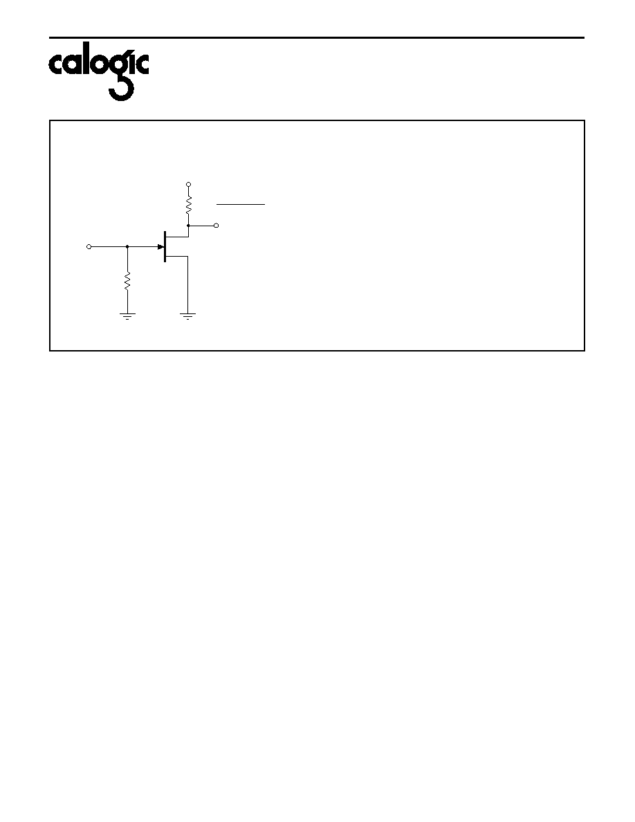
SWITCHING TIME, TEST CIRCUIT
D
S
=
R
L
V
IN
50
R
G
V
OUT
V
DD
0090
D(ON)
I
V
DS(ON)
-
V
DD
SAMPLING SCOPE
INPUT PULSE
RISE TIME 0.4ns
INPUT RESISTANCE 10M
INPUT CAPACITANCE 1.5pF
FALL TIME 0.75ns
PULSE WIDTH 200ns
PULSE RATE 550pps
RISE TIME 0.25ns