N-Channel Enhancement-Mode
MOS Transistor
2N7000 / BS170L
DESCRIPTION
The 2N7000 utilizes Calogic's vertical DMOS technology. The
device is well suited for switching applications where B
V
of
60V and low on resistance (under 5 ohms) are required. The
2N7000 is housed in a plastic TO-92 package.
ORDERING INFORMATION
Part
Package
Temperature Range
2N7000
Plastic TO-92
-55
o
C to +150
o
C
BS170L
Plastic TO-92
-55
o
C to +150
o
C
X2N7000
Sorted Chips in Carriers
-55
o
C to +150
o
C
CORPORATION
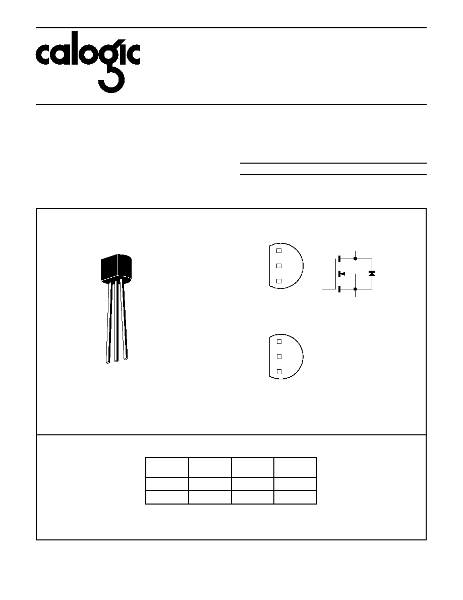
1 2
3
TO-92
(TO-226AA)
BOTTOM VIEW
1
2
3
1
2
3
SOURCE
GATE
DRAIN
1
2
3
2N7000
PIN CONFIGURATION
PRODUCT SUMMARY
P/N
V
(BR)DSS
(V)
r
DS(ON)
(
)
I
D
(A)
2N7000
60
5
0.2
BS170
60
5
0.5
CD5
BOTTOM VIEW
1
2
3
1
2
3
DRAIN
GATE
SOURCE
3
2
1
BS170L

2N7000 / BS170L
CORPORATION
ABSOLUTE MAXIMUM RATINGS (T
A
= 25
o
C unless otherwise specified)
SYMBOL
PARAMETERS
LIMITS
UNITS
TEST CONDITIONS
V
DS
Drain-Source Voltage
60
V
V
GS
Gate-Source Voltage
±
40
I
D
Continuous Drain Current
0.2
A
T
A
= 25
o
C
0.13
T
A
= 100
o
C
I
DM
Pulsed Drain Current
1
0.5
P
D
Power Dissipation
1
0.4
W
T
A
= 25
o
C
0.16
T
A
= 100
o
C
T
J
Operating Junction Temperature Range
-55 to 150
o
C
T
stg
Storage Temperature Range
-55 to 150
T
L
Lead Temperature (1/16" from case for 10 sec.)
300
THERMAL RESISTANCE RATINGS
SYMBOL
THERMAL RESISTANCE
LIMITS
UNITS
R
thJA
Junction-to-Ambient
312.5
K/W
NOTE:
1. Pulse width limited by maximum junction temperature.
SPECIFICATIONS
1
SYMBOL
PARAMETER
MIN
TYP
2
MAX
UNIT
TEST CONDITIONS
STATIC
V
(BR)DSS
Drain-Source Breakdown Voltage
60
70
V
I
D
= 10
µ
A, V
GS
= 0V
V
GS(th)
Gate-Threshold Voltage
0.8
1.9
3
V
DS
= V
GS
, I
D
= 1mA
I
GSS
Gate-Body Leakage
±
10
nA
V
GS
=
±
15V, V
DS
= 0V
I
DSS
Zero Gate Voltage Drain Current
1
µ
A
V
DS
= 48V, V
GS
= 0V
1000
T
C
= 125
o
C
I
D(ON)
On-State Drain Current
3
75
210
mA
V
DS
= 10V, V
GS
= 4.5V
r
DS(ON)
Drain-Source On-Resistance
3
4.8
5.3
4
V
GS
= 4.5V, I
D
= 75mA
2.5
5
V
GS
= 10V, I
D
= 0.5A
4.4
9
T
C
= 125
o
C
V
DS(ON)
Drain-Source On-Voltage
3
0.36
0.4
V
4
V
GS
= 4.5V, I
D
= 75mA
1.25
2.5
V
GS
= 10V, I
D
= 0.5A
2.2
4.5
T
C
= 125
o
C
4
g
FS
Forward Transconductance
3
100
170
mS
V
DS
= 10V, I
D
= 0.2A
g
OS
Common Source Output Conductance
3, 4
500
µ
S
V
DS
= 5V, I
D
= 50mA
DYNAMIC
C
iss
Input Capacitance
16
60
pF
V
DS
= 25V, V
GS
= 0V, f = 1MHz
C
oss
Output Capacitance
4
11
25
C
rss
Reverse Transfer Capacitance
2
5
SWITCHING
t
ON
Turn-On Time
7
10
nS
V
DD
= 15V, R
L
= 25
, I
D
= 0.5A
V
GEN
= 10V, R
G
= 25
(Switching time is essentially
independent of operating temperature)
t
OFF
Turn-Off Time
7
10
NOTES: 1.
T
A
= 25
o
C unless otherwise specified.
2. For design aid only, not subject to production testing.
3. Pulse test; PW =
300
µ
S, duty cycle
3%.
4. This parameter not registered with JEDEC.