HPR1XX REV M 4/03
1
Product: www.cdpoweronline.com
The HPR1XX Series uses advanced
circuit design and packaging technol-
ogy to deliver superior reliability and
performance. A 170kHz push-pull
oscillator is used in the input stage.
Beat-frequency oscillation problems are
reduced when using the HPR1XX Series
with high frequency isolation amplifiers.
Reduced parts count and high
efficiency add to the reliability of the
HPR1XX Series. The high efficiency of
the HPR1XX Series means less internal
power dissipation, as low as 190mW.
With reduced heat dissipation the
HPR1XX Series can operate at higher
temperatures with no degradation. In
addition, the high efficiency of the
HPR1XX Series means the series is able
to offer greater than 10 W/inch
3
of
output power density. Operation down
Corporate: www.cdtechno.com
Product: www.cdpoweronline.com
to no load will not impact the reliability
of the series, although a >1mA minimum
load is needed to realize published
specifications.
The HPR1XX Series provides the user
a low cost converter without sacrificing
reliability. The use of surface mounted
devices and advanced manufacturing
technologies make it possible to offer
premium performance and low cost.
NOMINAL
RATED
RATED
INPUT CURRENT
REFLECTED
INPUT
OUTPUT
OUTPUT
RIPPLE
VOLTAGE
VOLTAGE
CURRENT
NO LOAD
RATED LOAD
CURRENT
EFFICIENCY
MODEL
(VDC)
(VDC)
(mA)
(mA)
(mA)
(mAp-p)
(%)
HPR100
5
5
150
20
216
10
69
HPR101
5
12
62
20
212
5
70
HPR102
5
15
50
20
212
5
71
HPR103
5
�5
�75
20
218
5
68
HPR104
5
�12
�30
20
212
5
68
HPR105
5
�15
�25
20
200
5
75
HPR106
12
5
150
10
90
5
69
HPR107
12
12
62
10
81
5
77
HPR108
12
15
50
10
81
5
77
HPR109
12
�5
�75
10
88
5
71
HPR110
12
�12
�30
10
81
5
74
HPR111
12
�15
�25
10
81
5
77
HPR112
15
5
150
8
72
5
69
HPR113
15
12
62
8
72
5
69
HPR114
15
15
50
8
72
5
69
HPR115
15
�5
�75
8
72
5
69
HPR116
15
�12
�30
8
63
5
76
HPR117
15
�15
�25
8
63
5
79
HPR118
24
5
150
8
48
15
65
HPR119
24
12
62
8
48
15
65
HPR120
24
15
50
8
45
15
76
HPR121
24
�5
�75
8
45
15
69
HPR122
24
�12
�30
8
45
15
67
HPR123
24
�15
�25
8
45
15
69
Note: Other input to output voltages may be available. Please contact factory.
PRODUCT SELECTION CHART
0.75 Watt Single Output DC/DC Converter
HPR1XX
Low Cost
Multiple Package Styles
Internal Input and Output
Filtering
Non-Conductive Case
High Output Power Density:
10 Watts/Inch
3
Extended Temperature Range:
-25�C to +85�C
Efficiency to 79%
SPECIFICATIONS
All specifications are typical at T
A
= +25�C nominal input voltage unless otherwise specified.
HPR1XX REV M 4/03
2
Product: www.cdpoweronline.com
50
100
150
200
250
TEMPERA
TURE (�C)
TIME (seconds)
235 �C MAX
220
190
30 sec MAX
(>220�C)
90 sec MAX
(>190�C)
0.730"
(18.54)
0.650"
(16.51)
0.100"
(2.54)
0.080"
(2.03)
0.040"
(1.02)
14 13
11 10
3
2
1
4
7
6
5
9 8
RECOMMENDED REFLOW PROFILE
RECOMMENDED LAND PATTERN
SPECIFICATIONS, ALL MODELS
Specifications are at T
A
= +25�C nominal input voltage unless otherwise specified.
GENERAL OUTPUT
INPUT
PARAMETER
CONDITIONS
MIN
TYP
MAX
UNITS
INPUT
Voltage Range
4.5
5
5.5
VDC
10.8
12
13.2
VDC
13.5
15
16.5
VDC
21.6
24
26.4
VDC
Voltage Rise Time See Typical Performance Curves & Application Notes: "Capacitive Loading Effects on Start-Up of DC/DC Converters"
OUTPUT
Rated Power
750
mW
Voltage Setpoint Accuracy
Rated Load, Nominal V
IN
�5
%
Ripple & Noise
BW = DC to 10MHz
45
mVp-p
BW =10Hz to 2MHz
30
mVrms
HPR103
BW = DC to 10MHz
90
mVp-p
Voltage (Over Input Voltage Range)
1mA Load, V
OUT
= 5V
7
VDC
1mA Load, V
OUT
= 12V
15
VDC
1mA Load, V
OUT
= 15V
18
VDC
Temperature Coefficent
.01
%/�C
REGULATION
Line Regulation
High Line to Low Line
1
%/%Vin
GENERAL
ISOLATION
Rated Voltage
750
VDC
Test Voltage
60 Hz, 10 Seconds
750
Vrms (1060pk)
Resistance
10
G
Capacitance
25
100
pF
Leakage Current
V
ISO
= 240VAC, 60Hz
2
8.5
�
Arms
Switching Frequency
170
kHz
Frequency Change
Over Line and Load
24
%
Package Weight
2
g
MTTF per MIL-HDBK-217, Rev. E*
Circuit Stress Method
Ground Benign
T
A
= +25�C
7.9
MHr
Fixed Ground
T
A
= +35�C
1.9
MHr
Naval Sheltered
T
A
= +35�C
1.2
MHr
Airborne Uninhabited Fighter
T
A
= +35�C
300
kHr
TEMPERATURE
Specification
-25
+25
+85
�C
Operation
-40
+100
�C
Storage
-40
+110
�C
* For demonstrated MTTF results reference: Power Convertibles Reliability Report HPR105.
HPR1XX REV M 4/03
3
Product: www.cdpoweronline.com
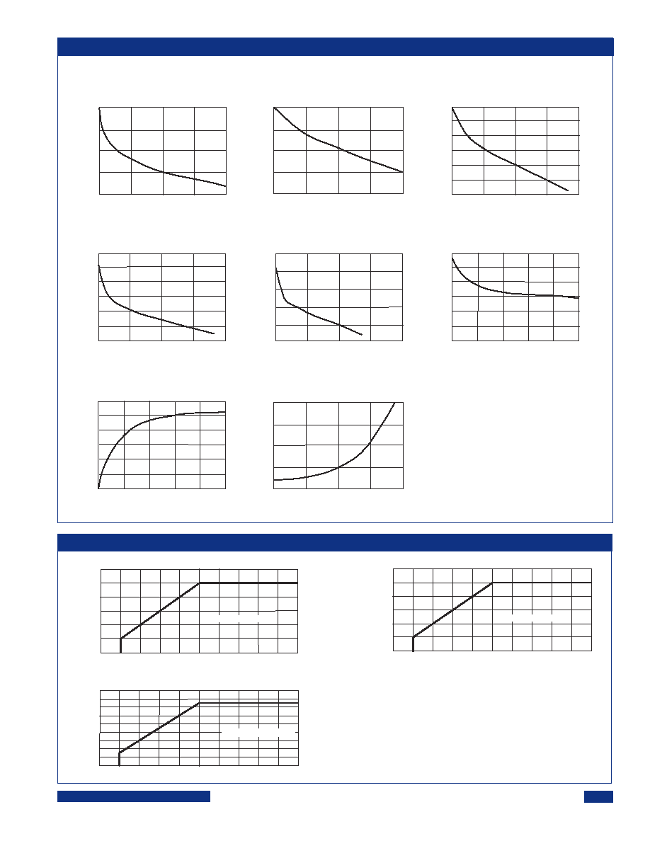
VOUT VS LOAD
(5Vout Models)
VOUT VS LOAD
(�5Vout Models)
VOUT VS LOAD
(12Vout Models)
VOUT VS LOAD
(�12Vout Models)
VOUT VS LOAD
(15Vout Models)
VOUT VS LOAD
(�15Vout Models)
0
40
120
160
5.3
5.5
5.7
4.9
5.1
0
20
40
60
80
11.9
12.0
12.1
12.2
12.3
12.4
0
20
40
60
80
4.6
4.8
5.0
5.2
5.4
0
10
20
30
40
12.0
12.1
12.2
12.3
12.4
12.5
14.9
15.1
15.3
15.5
15.7
15.9
0
20
40
60
80
0
13.5
14.0
14.5
15.0
15.5
16.0
V
out
V
out
V
out
V
out
V
out
V
out
F
requency (KHz)
80
Output Current (mA)
Output Current each load (mA)
Output Current each load (mA)
12.5
Output Current each load (mA)
12.6
Output Current each load (mA)
Output Power each load (Watts)
0.2
0.4
0.6
0.8
1.0
16.5
0
40
80
100
60
20
90
75
60
45
30
15
0
EFFICIENCY VS LOAD
% of Rated Load (%)
Ef
ficiency (%)
OSCILLATION FREQUENCY VS
TEMPERATURE
220
200
180
160
140
-30
0
30
60
90
Temperature (�C)
SAFE OPERATING AREA
Rise Time of Input Voltage (mS)
LOAD CAPACITANCE vs INPUT RISE TIME
(5 Vout models)
T
o
tal Load Capacitance (uF)
0 5 10 15 20 25 30 35 40 45 50
600
500
400
300
200
100
0
SAFE OPERATING AREA
Rise Time of Input Voltage (mS)
LOAD CAPACITANCE vs INPUT RISE TIME
(12 Vout models)
T
o
tal Load Capacitance (uF)
0 5 10 15 20 25 30 35 40 45 50
90
80
70
60
50
40
30
20
10
0
SAFE OPERATING AREA
Rise Time of Input Voltage (mS)
LOAD CAPACITANCE vs INPUT RISE TIME
(15 Vout models)
T
otal Load Capacitance (uF)
0 5 10 15 20 25 30 35 40 45 50
60
50
40
30
20
10
0
NOTES:
1.) When operated within the SAFE OPERATING AREA as defined
by the above curves, the output voltage of HPR1XX devices is
guaranteed to be within 95% of its steady-state value within 100
milliseconds after the input voltage has reached 95% of its steady-
state value.
2.) For dual output models, total load capacitance is the sum of the
capacitances on the plus and minus outputs.
Specifications are at T
A
= +25�C nominal input voltage, nominal load, recommended external components applied, unless
otherwise specified. (Refer to Application Note DCAN-9 at www.cdpoweronline.com)
TYPICAL PERFORMANCE CURVES
SAFE OPERATING AREA
HPR1XX REV M 4/03
4
Product: www.cdpoweronline.com
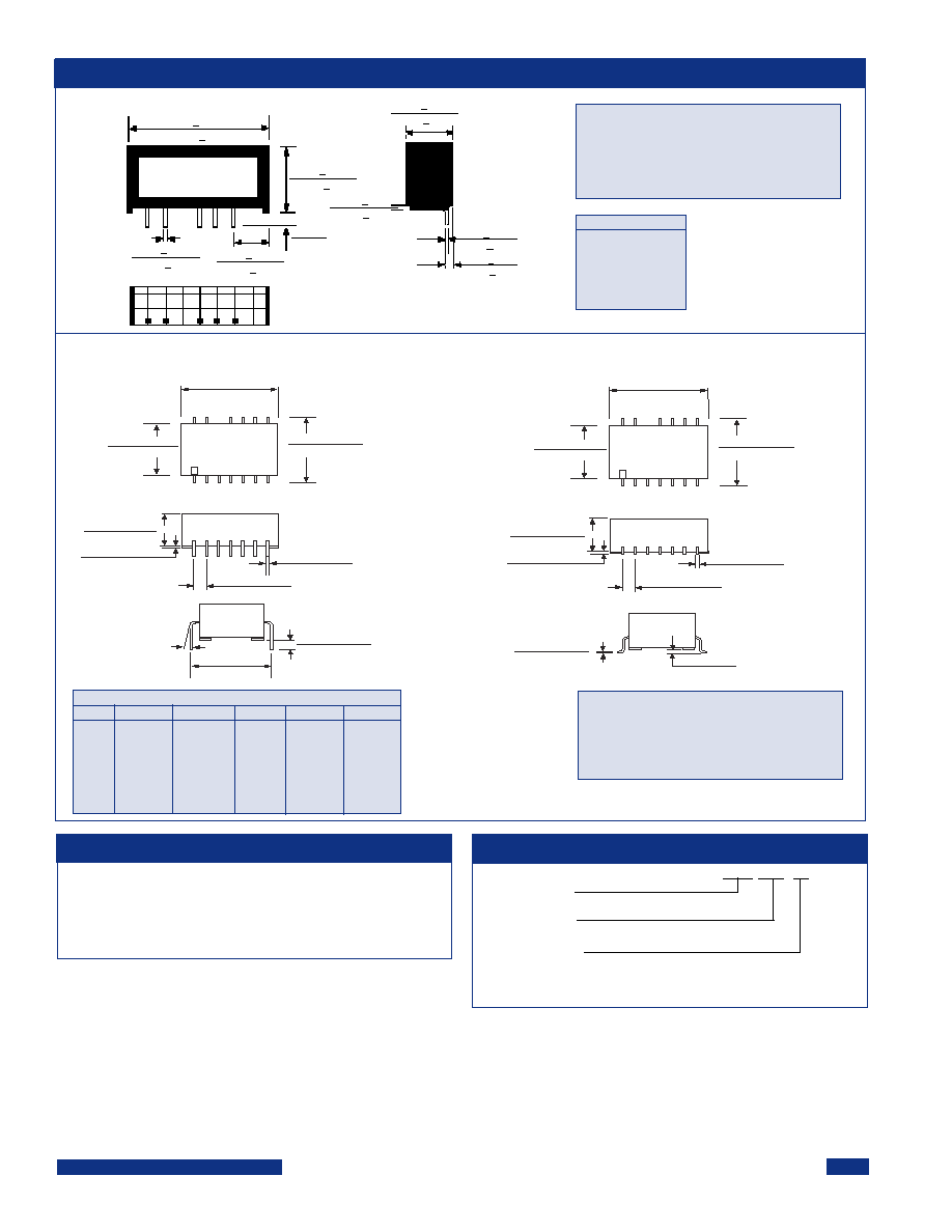
PIN CONNECTIONS
1.
+VIN
2.
-VIN
4.
-VOUT
5.
COM*
6.
+VOUT
PACKAGE/PINOUT "V" AND "W"
0.100�0.010"
(2.54�0.25)
0.020�0.002"
(0.51�0.05)
0.015�0.005"
(0.38�0.13)
0.375�0.005"
(9.52�0.13)
0.785�0.010"
(19.94�0.25)
14 13
11 10
3
2
1
4
7
6
5
9 8
0.525�0.010"
(13.34�0.25)
0.695�0.015"
(17.65�0.38)
0.014�0.002"
(0.36�0.05)
.015�.010"
(.38�.26)
0.100�0.010"
(2.54�0.25)
0.020�0.002"
(0.51�0.05)
0.015�0.005"
(0.38�0.13)
0.375�0.005"
(9.52�0.13)
0�-
15
�
0.125+0.030"
-0.000"
(3.18+0.76)
( -0.00)
0.785�0.010"
(19.94�0.25)
14 13
11 10
3
2
1
4
7
6
5
9 8
0.525�0.010"
(13.34�0.25)
0.695�0.015"
(17.65�0.38)
0.600"
(15.24)
DIP PACKAGE
SMD PACKAGE
END VIEWS
SIDE VIEWS
TOP VIEWS
HPR1XXV
HPR1XXW
"SIP" PACKAGE/PINOUT
Notes:
All dimensions are in inches (millimeters).
GRID: 0.100 inches (2.54 millimeters)
PIN PLACEMENT TOLERANCE: � 0.015"
*Common pin not present on single output models.
FRONT
VIEW
RIGHT
SIDE
VIEW
BOTTOM
VIEW
0.77 +0.010"
(19.56 +0.25)
0.02 +0.002"
(0.51 +0.05)
0.18 +0.015"
(4.57 +0.38)
0.140"
(3.56)
MIN
1 2 4 *5 6
0.400 +0.010"
(10.16 +0.25)
0.240 +0.010"
(6.09 +0.25)
0.020 +0.010"
(0.51 +0.25)
0.01 +0.002"
(0.25 +0.05)
0.035 +0.015"
(0.89 +0.38)
MECHANICAL
NOTES:
NC = Do Not Connect.
Duplicate pin functions are internally connected.
All dimensions are in inches (millimeters).
GRID: 0.100 inches (2.54 millimeters)
Internal Power Dissipation ................................. 450mW
ShortCircuitDuration ........................................... Momentary
Lead Temperature (soldering, 10 seconds max .+300�C *
* NOTE: Refer to Reflow Profile for SMD Models.
ABSOLUTE MAXIMUM RATINGS
HPR 1XX V/W
Device Family
HPR Indicates DC/DC Converter
Model Number
Selected from Table of Electrical Characteristics
Package Option
There is "no" package designator for the SIP package
V = DIP Package
W = SMD Package
ORDERING INFORMATION
PIN CONNECTIONS
PIN# SINGLES DUALS
1
+VIN
+VIN
2
-VIN
-VIN
3
NC
NC
4
NC
NC
5
-VOUT
-VOUT
6
NC
Common
PIN# SINGLES DUALS
7
+VOUT
+VOUT
8
NC
NC
9
NC
NC
10
NC
NC
11
NC
NC
13
NC
NC
14
NC
NC
Any data, prices, descriptions or specifications presented herein are subject to revision by C&D Technologies, Inc. without notice. While such information is believed to
be accurate as indicated herein, C&D Technologies, Inc. makes no warranty and hereby disclaims all warranties, express or implied, with regard to the accuracy or
completeness of such information. Further, because the product(s) featured herein may be used under conditions beyond its control, C&D Technologies, Inc. hereby
disclaims all warranties, either express or implied, concerning the fitness or suitability of such product(s) for any particular use or in any specific application or arising
from any course of dealing or usage of trade. The user is solely responsible for determining the suitability of the product(s) featured herein for user's intended purpose
and in user's specific application. C&D Technologies, Inc. does not warrant or recommend that any of its products be used in any life support or aviation or aerospace
applications.
Power Electronics Division, Americas
3400 E Britannia Drive, Tucson, Arizona 85706
Tel: 800.547.2537 Fax: 520.295.4197
C&D Technologies, EMEA/AP
Milton Keynes MK14 5BU UK
Tel: +44 (0)1908 615232
Fax: +44 (0)1908 617545