NEC'
S
3.2 V, 3 W, L/S BAND
MEDIUM POWER SILICON LD-MOSFET
California Eastern Laboratories
FEATURES
∑ LOW COST PLASTIC SURFACE MOUNT PACKAGE
∑ HIGH OUTPUT POWER: +35.5 dBm TYP
∑ HIGH LINEAR GAIN: 16 dB TYP @ 915 MHz
∑ HIGH POWER ADDED EFFICIENCY: 65% TYP @
V
DS
= 3.2 V, f = 915 MHz
∑ SINGLE SUPPLY: 2.8 to 6.0 V
∑ CLASS AB OPERATION
∑ SURFACE MOUNT PACKAGE: 5.7
x
5.7
x
1.1 mm MAX
NE5520379A
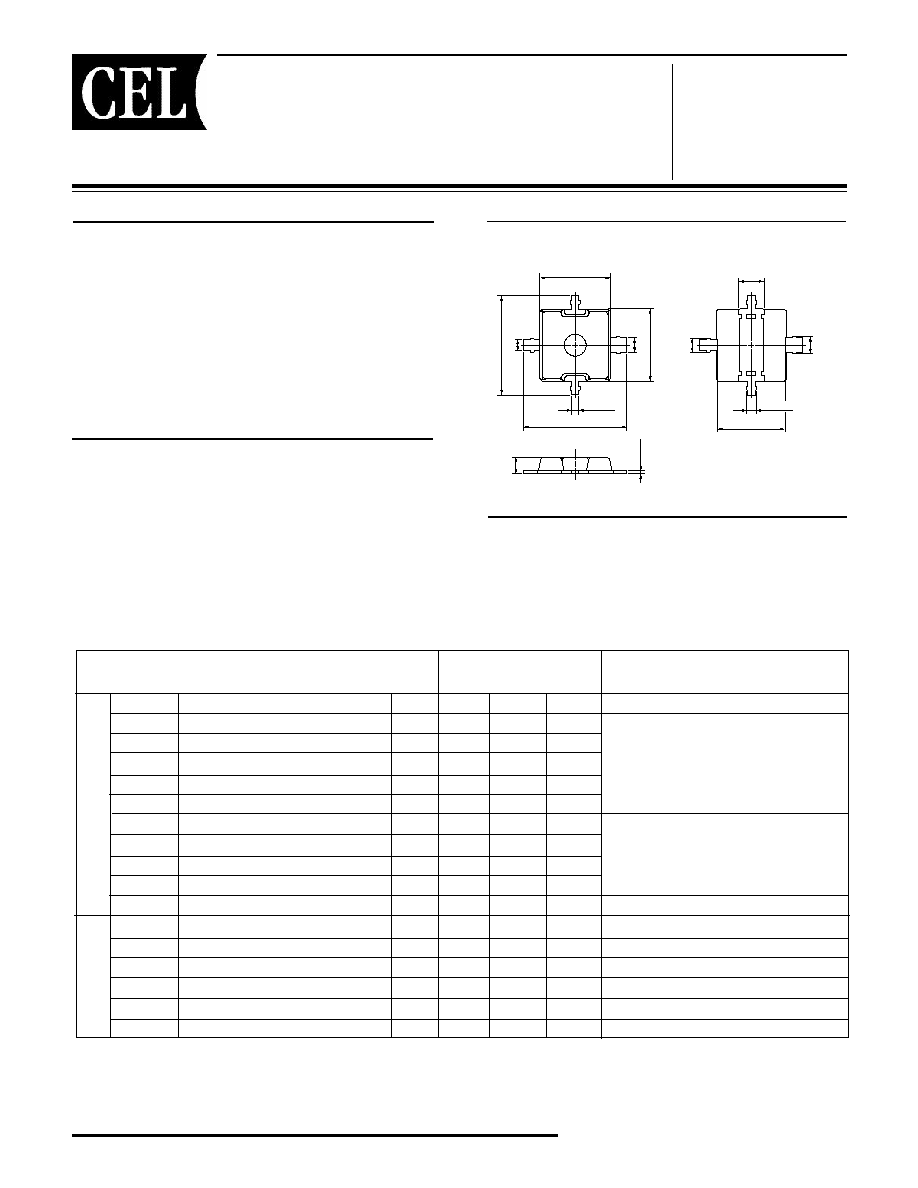
OUTLINE DIMENSIONS
(Units in mm)
PACKAGE OUTLINE 79A
DESCRIPTION
NEC's NE5520379A is an N-Channel silicon power MOSFET
specially designed as the transmission power amplifier for
3.2 V GSM900 handsets. Die are manufactured using NEC's
NEWMOS technology (NEC's 0.6 m WSi gate lateral MOS-
FET) and housed in a surface mount package. This device
can deliver 35.5 dBm output power at 915 MHz and 3.2 V, or
34.6 dBm output power at 2.8 V by varying the gate voltage
as a power control function.
Note:
1. DC performance is tested 100%. Several samples per wafer are tested for RF performance. Wafer rejection criteria for standard devices is 1
reject for several samples.
ELECTRICAL CHARACTERISTICS
(T
A
= 25∞C)
PART NUMBER
NE5520379A
PACKAGE OUTLINE
79A
SYMBOLS
CHARACTERISTICS
UNITS MIN
TYP
MAX
TEST CONDITIONS
P
OUT
Output Power
dBm
35.5
G
L
Linear Gain
(at P
IN
= +10 dBm)
dB
16.0
D
Drain Efficiency
%
68
ADD
Power Added Efficiency
%
65
I
D
Operating Drain Current
A
1.0
P
OUT
Output Power
dBm
31.0
33.0
G
L
Linear Gain
(at P
IN
= +10 dBm)
dB
8.5
I
D
Operating Drain Current
mA
750
D
Drain Efficiency
%
29
38
ADD
Power Added Efficiency
%
35
I
GSS
Gate-to-Source Leakage Current
nA
100
V
GS
= 6.0 V
I
DSS
Drain-to-Source Leakage Current
nA
100
V
DS
= 8.5 V
V
TH
Gate Threshold Voltage
V
1.0
1.35
2.0
V
DS
= 3.5 V, I
DS =
1 mA
gm
Transconductance
S
2.5
V
DS
= 3.5 V, I
DS1 =
0.8 A, I
DS2 =
1.0 A
BV
DSS
Drain-to-Source Breakdown Voltage
V
15
20
I
DSS
= 10 µA
R
TH
Thermal Resistance
∞
C/W
5
Channel-to-Case
Functional Characteristics
Electrical DC Characteristics
f = 915 MHz, V
DS
= 3.2 V,
V
GS
= 2.5 V(RF OFF)
(NOTE 1)
f = 1785 MHz, V
DS
= 3.2 V,
V
GS
= 2.5 V
(NOTE 1)
∑ DIGITAL CELLULAR PHONES:
3.2 V GSM900/DCS 1800 Dual Band Handsets
∑ OTHERS:
Two-Way Pagers
Retail Business Radio
Special Mobile Radio
Short Range Wireless
APPLICATIONS
0.9±0.2
0.2±0.1
(Bottom View)
3.6±0.2
1.5±0.2
1.2 MAX.
0.8 MAX.
1.0 MAX.
Source
Gate
Drain
0.4±0.15
5.7 MAX.
5.7 MAX.
0.6±0.15
0.8±0.15
4.4 MAX.
4.2 MAX.
Source
Gate
Drain
A
3
9Z001

ABSOLUTE MAXIMUM RATINGS
1
(T
A
= 25 ∞C)
SYMBOLS
PARAMETERS
UNITS RATINGS
V
DS
Drain to Source Voltage
V
15.0
V
GS
Gate to Source Voltage
V
5.0
I
D
Drain Current
A
1.5
I
D
Drain Current (Pulse Test)
2
A
3.0
P
T
Total Power Dissipation
W
20
T
CH
Channel Temperature
∞C
125
T
STG
Storage Temperature
∞C
-65 to +125
RECOMMENDED OPERATING LIMITS
SYMBOLS PARAMETERS
UNITS TYP MAX
V
DS
Drain to Source Voltage V
3.2
6.0
V
GS
Gate to Source Voltage
V
2.5
3.5
I
DS
Drain Current (Pulse Test) A
1.75
2.0
P
IN
Input Power
dBm
25
26
Note:
1. Operation in excess of any one of these parameters may result
in permanent damage.
2. Duty Cycle 50%, Ton 1 s.
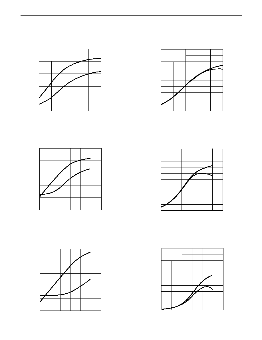
TYPICAL PERFORMANCE CURVES
(T
A
= 25∞C)
PART NUMBER
QTY
NE5520379A-T1A-A
ORDERING INFORMATION
Drain Current, I
D
(A)
DRAIN CURRENT vs.
DRAIN TO SOURCE VOLTAGE
Drain to Source Voltage, V
DS
(V)
4.0
1.0
2.0
1.5
3.5
2.5
3.0
0.5
0
10
9
7
8
6
5
3
4
1
2
3.6 V
3.4 V
3.2 V
3.0 V
2.8 V
2.6 V
2.4 V
2.2 V
2.0 V
Quiescent Drain Current, I
D
(A)
QUIESCENT DRAIN CURRENT vs.
GATE TO SOURCE VOLTAGE
Gate to Source Voltage, V
GS
(V)
V
DS
= 3.2 V
10 000
100
1 000
10
1
3.0
2.5
2.0
1.5
1.0
NE5520379A
NE5520379A
TYPICAL PERFORMANCE CURVES
(T
A
= 25∞C)
V
DS
= 3.2 V
I
DSQ
= 600 mA
f = 915 MHz
P
out
I
D
40
25
35
30
20
15
2 500
2 000
1 500
1 000
500
0
35
30
20
15
10
5
25
V
DS
= 3.2 V
I
DSQ
= 600 mA
f = 915 MHz
d
add
100
50
0
35
30
25
20
15
10
5
V
DS
= 3.2 V
I
DSQ
= 600 mA
f = 1 785 MHz
P
out
I
D
35
20
30
25
15
10
2 500
2 000
1 500
1 000
500
0
35
30
20
15
10
5
25
V
DS
= 3.2 V
I
DSQ
= 600 mA
f = 1 785 MHz
d
add
100
50
0
35
30
25
20
15
10
5
Drain Efficiency ,
d
(%)
Powwer
Added Efficiency
,
add
(%)
DRAIN EFFICIENCY, POWER ADDED
EFFICIENCY vs. INPUT POWER
Input Power, P
in
(dBm)
Output Power
, P
out
(dBm)
OUTPUT POWER, DRAIN CURRENT
vs. INPUT POWER
Input Power, P
in
(dBm)
Drain Efficiency ,
d
(%)
Powwer
Added Efficiency
,
add
(%)
DRAIN EFFICIENCY, POWER ADDED
EFFICIENCY vs. INPUT POWER
Input Power, P
in
(dBm)
Drain Current, I
D
(mA)
2500
2000
1500
1000
500
0
0
15
20
25
30
35
40
V
DS
= 3.6 V
I
Dset
= 150 mA
f = 460 MHz
5
10
15
20
25
P
out
I
D
100
50
0
0
5
10
15
20
25
V
DS
= 3.6 V
I
Dset
= 150 mA
f = 460 MHz
d
add
Output Power
, P
out
(dBm)
OUTPUT POWER, DRAIN CURRENT
vs. INPUT POWER
Input Power, P
in
(dBm)
Drain Current, I
D
(mA)
Output Power
, P
out
(dBm)
OUTPUT POWER, DRAIN CURRENT
vs. INPUT POWER (460 MHz)
Input Power, P
in
(dBm)
Drain Current, I
D
(mA)
Drain Efficiency ,
d
(%)
Powwer
Added Efficiency
,
add
(%)
DRAIN EFFICIENCY, POWER ADDED
EFFICIENCY vs. INPUT POWER
Input Power, P
in
(dBm)

V
DS
= 3.2 V
f = 915 MHz
P
in
= 25 dBm
P
out
I
D
36
33
35
34
32
31
2 500
2 000
1 500
1 000
500
0
4.0
2.0
1.0
0.0
3.0
V
DS
= 3.2 V
f = 1 785 MHz
P
in
= 25 dBm
P
out
I
D
33
27
31
29
25
23
2 500
2 000
1 500
1 000
500
0
4.0
2.0
1.0
0.0
3.0
Output Power
, P
out
(dBm)
OUTPUT POWER, DRAIN CURRENT
vs. GATE TO SOURCE VOLTAGE
Gate to Source Voltage, V
GS
(V)
Output Power
, P
out
(dBm)
OUTPUT POWER, DRAIN CURRENT
vs. GATE TO SOURCE VOLTAGE
Gate to Source Voltage, V
GS
(V)
Drain Current, I
D
(mA)
Drain Current, I
D
(mA)
NE5520379A
TYPICAL PERFORMANCE CURVES
(T
A
= 25∞C)

NE5520379A
TYPICAL SCATTERING PARAMETERS
(T
A
= 25∞C)
FREQUENCY
S
11
S
21
S
12
S
22
K
MAG
1
GHz
MAG ANG
MAG ANG
MAG
ANG
MAG ANG
(dB)
0.10
0.91
-166.00
4.96
91.46
0.02
2.83
0.87
-177.51
0.12
24.77
0.15
0.91
-171.34
3.32
86.63
0.02
-3.69
0.87
-178.85
0.16
22.87
0.20
0.91
-174.19
2.48
82.34
0.02
-4.78
0.87
-179.72
0.24
21.67
0.25
0.91
-176.05
1.98
78.94
0.02
-7.98
0.87
179.68
0.29
20.65
0.30
0.92
-177.47
1.63
75.61
0.02 -9.01
0.87
179.13
0.37
19.83
0.35
0.92
-178.62
1.39
72.51
0.02
-11.04
0.87
178.64
0.44
19.13
0.40
0.92
-179.56
1.20
69.74
0.02
-14.40
0.88
178.26
0.50
18.71
0.45
0.92
179.62
1.06
66.85
0.02
-16.23
0.88
177.80
0.56
18.21
0.50
0.92
178.83
0.94
64.15
0.02
-18.73
0.88
177.43
0.63
17.79
0.55
0.92
178.12
0.85
61.50
0.02
-20.26
0.88
176.97
0.71
17.43
0.60
0.92
177.42
0.77
58.92
0.01
-19.69
0.88
176.61
0.87
17.25
0.65
0.93
176.76
0.70
56.40
0.01
-22.40
0.89
176.14
0.86
16.77
0.70
0.93
176.09
0.64
53.87
0.01
-24.70
0.89
175.63
0.93
16.44
0.75
0.93
175.48
0.59
51.57
0.01
-26.30
0.89
175.27
1.05
14.89
0.80
0.93
174.86
0.54
49.32
0.01
-27.01
0.89
174.81
1.12
13.95
0.85
0.93
174.22
0.50
46.99
0.01
-28.40
0.89
174.31
1.27
12.74
0.90
0.93
173.60
0.47
44.90
0.01
-29.48
0.90
173.93
1.33
12.17
0.95
0.94
173.03
0.44
42.72
0.01
-31.03
0.90
173.42
1.44
11.53
1.00
0.94
172.43
0.41
40.69
0.01
-31.65
0.90
172.99
1.61
10.79
1.20
0.94
170.05
0.32
33.12
0.01
-35.32
0.91
171.08
2.08
8.96
1.30
0.95
168.90
0.28
29.64
0.01
-38.66
0.91
170.17
2.43
8.10
1.40
0.95
167.71
0.25
26.30
0.01
-40.07
0.91
169.12
2.88
7.18
1.50
0.95
166.62
0.23
23.15
0.01
-40.31
0.92
168.10
3.31
6.55
1.60
0.95
165.46
0.21
20.23
0.01
-42.08
0.92
167.21
4.05
5.86
1.70
0.95
164.33
0.19
17.61
0.01
-41.45
0.92
166.35
4.91
5.12
1.80
0.96
163.28
0.17
15.02
0.01
-41.35
0.92
165.39
5.68
4.38
1.90
0.96
162.22
0.16
12.55
0.00
-40.16
0.93
164.37
7.09
3.84
2.00
0.96
161.21
0.14
10.37
0.00
-35.50
0.93
163.55
8.29
3.46
2.10
0.96
160.17
0.13
8.42
0.00
-30.05
0.93
162.80
11.07
2.90
2.20
0.96
159.17
0.12
6.46
0.00
-21.25
0.93
161.93
14.89 2.19
2.30
0.96
158.29
0.11
4.59
0.00
-15.26
0.94
160.98
16.85
1.67
2.40
0.96
157.41
0.11
3.14
0.00
-1.99
0.94
160.15
18.02
1.65
2.50
0.97
156.53
0.10
1.92
0.00
9.51
0.95
159.57
16.22
1.49
2.60
0.97
155.72
0.09
0.69
0.00
17.40
0.95
158.86
18.87
0.98
2.70
0.97
154.92
0.09
-0.82
0.00
49.62
0.95
158.02
17.17
0.60
2.80
0.97
154.17
0.08
-2.13
0.00
54.56
0.95
157.17
17.91
0.80
2.90
0.97
153.44
0.08
-3.31
0.00
75.69
0.96
156.56 11.30 0.89
3.00
0.97
152.77
0.07
-4.03
0.00
84.78
0.96
155.94
12.00
0.68
3.10
0.97
152.20
0.07
-4.64
0.00
91.22
0.97
155.48
7.64
0.86
3.20
0.98
151.52
0.06
-5.69
0.00
89.31
0.97
154.37
6.03
0.83
3.30
0.98
150.94
0.06
-5.93
0.00
94.43
0.98
153.79
4.52
1.47
3.40
0.98
150.36
0.06
-6.52
0.01
93.75
0.98
153.16
3.50
1.69
3.50
0.98
149.78
0.05
-6.88
0.01
93.93
0.98
152.45
3.08
1.43
4.00
0.99
148.45
0.04
-5.44
0.01
93.64
0.99
150.04
1.13
4.11
NE5520379A
V
D
= 2.4 V, I
D
= 300 mA
Coordinates in Ohms
Frequency in GHz
V
D
=
2.4 V, I
D
= 300
mA
Note: This file and many other s-parameter files can be downloaded from www.cel.com
j50
j25
j10
0
-j10
-j25
-j50
-j100
j100
0
10
25
50
100
120∞
90∞
60∞
30∞
150∞
180∞
-150∞
-120∞
-90∞
-60∞
-30∞
0∞
MAG = Maximum Available Gain
MSG = Maximum Stable Gain
Note:
1. Gain Calculation:
MAG = |S
21
|
|S
12
|
K - 1
).
2
(
K ±
= S
11
S
22
- S
21
S
12
When K 1, MAG is undefined and MSG values are used. MSG = |S
21
|
|S
12
|
, K = 1 + | | - |S
11
| - |S
22
|
2
2
2
2 |S
12
S
21
|
,

NE5520379A
MAG = Maximum Available Gain
MSG = Maximum Stable Gain
Note:
1. Gain Calculation:
MAG = |S
21
|
|S
12
|
K - 1
).
2
(
K ±
= S
11
S
22
- S
21
S
12
When K 1, MAG is undefined and MSG values are used. MSG = |S
21
|
|S
12
|
, K = 1 + | | - |S
11
| - |S
22
|
2
2
2
2 |S
12
S
21
|
,
TYPICAL SCATTERING PARAMETERS
(T
A
= 25∞C)
Coordinates in Ohms
Frequency in GHz
V
D
=
3.0 V, I
D
= 600
mA
Note: This file and many other s-parameter files can be downloaded from www.cel.com
j50
j25
j10
0
-j10
-j25
-j50
-j100
j100
0
10
25
50
100
120∞
90∞
60∞
30∞
150∞
180∞
-150∞
-120∞
-90∞
-60∞
-30∞
0∞
FREQUENCY
S
11
S
21
S
12
S
22
K
MAG
1
GHz
MAG ANG
MAG ANG
MAG
ANG
MAG ANG
(dB)
0.10
0.93
-166.51
5.08
92.43
0.01
4.88
0.89
-178.46
0.14
26.14
0.15
0.93
-171.79
3.41
88.12
0.01
-2.92
0.89
-179.65
0.15
24.16
0.20
0.93
-174.68
2.54
84.33
0.01
-2.57
0.89
179.54
0.25
23.01
0.25
0.93
-176.58
2.03
81.48
0.01
-2.60
0.89
178.98
0.33
21.95
0.30
0.93
-178.04
1.69
78.54
0.01
-5.09
0.89
178.33
0.39
21.14
0.35
0.93
-179.24
1.44
75.97
0.01
-7.10
0.89
177.89
0.47
20.48
0.40
0.93
179.79
1.25
73.62
0.01
-9.56
0.89
177.44
0.52
20.03
0.45
0.93
178.92
1.11
71.09
0.01
-11.04
0.89
176.93
0.59
19.51
0.50
0.93
178.11
0.99
68.88
0.01
-12.64
0.89
176.63
0.68
19.16
0.55
0.94
177.36
0.89
66.51
0.01
-12.76
0.90
176.06
0.75
18.72
0.60
0.94
176.64
0.81
64.31
0.01
-13.34
0.89
175.72
0.93
18.57
0.65
0.94
175.96
0.75
62.14
0.01
-14.37
0.90
175.29
0.91
18.08
0.70
0.94
175.28
0.69
59.81
0.01
-16.01
0.90
174.68
1.02
17.03
0.75
0.94
174.66
0.63
57.87
0.01
-17.13
0.90
174.42
1.14
15.30
0.80
0.94
174.05
0.59
55.81
0.01
-16.95
0.90
173.89
1.18
14.78
0.85
0.94
173.41
0.55
53.68
0.01
-18.56
0.90
173.39
1.39
13.45
0.90
0.94
172.80
0.51
51.88
0.01
-19.71
0.90
173.13
1.40
13.11
0.95
0.94
172.21
0.48
49.77
0.01
-19.61
0.90
172.51
1.52
12.48
1.00
0.94
171.63
0.45
47.95
0.01
-19.95
0.90
172.16
1.71
11.68
1.10
0.94
170.41
0.40
44.15
0.01
-24.20
0.91
171.11
1.93
10.81
1.20
0.95
169.32
0.36
40.82
0.01
-23.13
0.91
170.30
2.13
10.08
1.30
0.95
168.20
0.32
37.55
0.01
-24.29
0.91
169.48
2.56
9.13
1.40
0.95
167.05
0.29
34.19
0.01
-25.78
0.91
168.40
3.14
8.10
1.50
0.95
166.00
0.27
30.96
0.01
-25.39
0.92
167.30
3.52
7.56
1.60
0.95
164.89
0.24
28.24
0.01
-25.03
0.92
166.57
4.07
7.05
1.70
0.95
163.80
0.22
25.67
0.01
-22.37
0.92
165.86
4.72
6.28
1.80
0.95
162.78
0.20
22.92
0.00
-20.35
0.92
164.91
6.13
5.28
1.90
0.96
161.76
0.19
20.12
0.00
-18.82
0.92
163.74
7.13
4.85
2.00
0.96
160.78
0.18
17.88
0.00
-12.65
0.93
162.96
7.85
4.65
2.10
0.96
159.78
0.16
16.09
0.00
-5.72
0.93
162.54
9.04
4.16
2.20
0.96
158.80
0.15
14.12
0.00
2.28
0.93
161.73
11.69
3.15
2.30
0.96
157.95
0.14
12.01
0.00
9.59
0.93
160.62
12.90
2.58
2.40
0.96
157.10
0.13
10.33
0.00
16.52
0.94
159.68
11.53
2.95
2.50
0.96
156.24
0.12
9.11
0.00
24.13
0.95
159.46
10.27
2.98
2.60
0.96
155.45
0.12
7.63
0.00
38.01
0.94
158.99
11.45
2.19
2.70
0.97
154.66
0.11
5.72
0.00
48.37
0.94
158.00
10.95
1.62
2.80
0.97
153.93
0.10
3.94
0.00
55.62
0.95
156.90
10.04
2.00
2.90
0.97
153.22
0.10
2.73
0.00
64.87
0.96
156.45
7.62
2.62
3.00
0.97
152.55
0.09
1.96
0.00
69.74
0.96
156.03
7.17
2.29
3.10
0.97
152.00
0.09
1.15
0.00
81.95
0.96
155.48
6.39
2.11
3.20
0.97
151.33
0.08 -0.21
0.00
80.85
0.97
154.23
5.03
2.21
3.30
0.98
150.77
0.08
-0.76
0.01
86.32
0.97
153.57
3.62
3.03
3.40
0.98
150.20
0.07 -1.47
0.01
86.22
0.98
153.08
3.20
3.00
3.50
0.98
149.63
0.07
-2.27
0.01
87.98
0.97
152.19
3.09
2.26
4.00
0.99
148.33
0.05
-2.98
0.01
88.38
0.98
149.87
1.37
3.81
NE5520379A
V
D
= 3.0 V, I
D
= 600 mA
NE5520379A
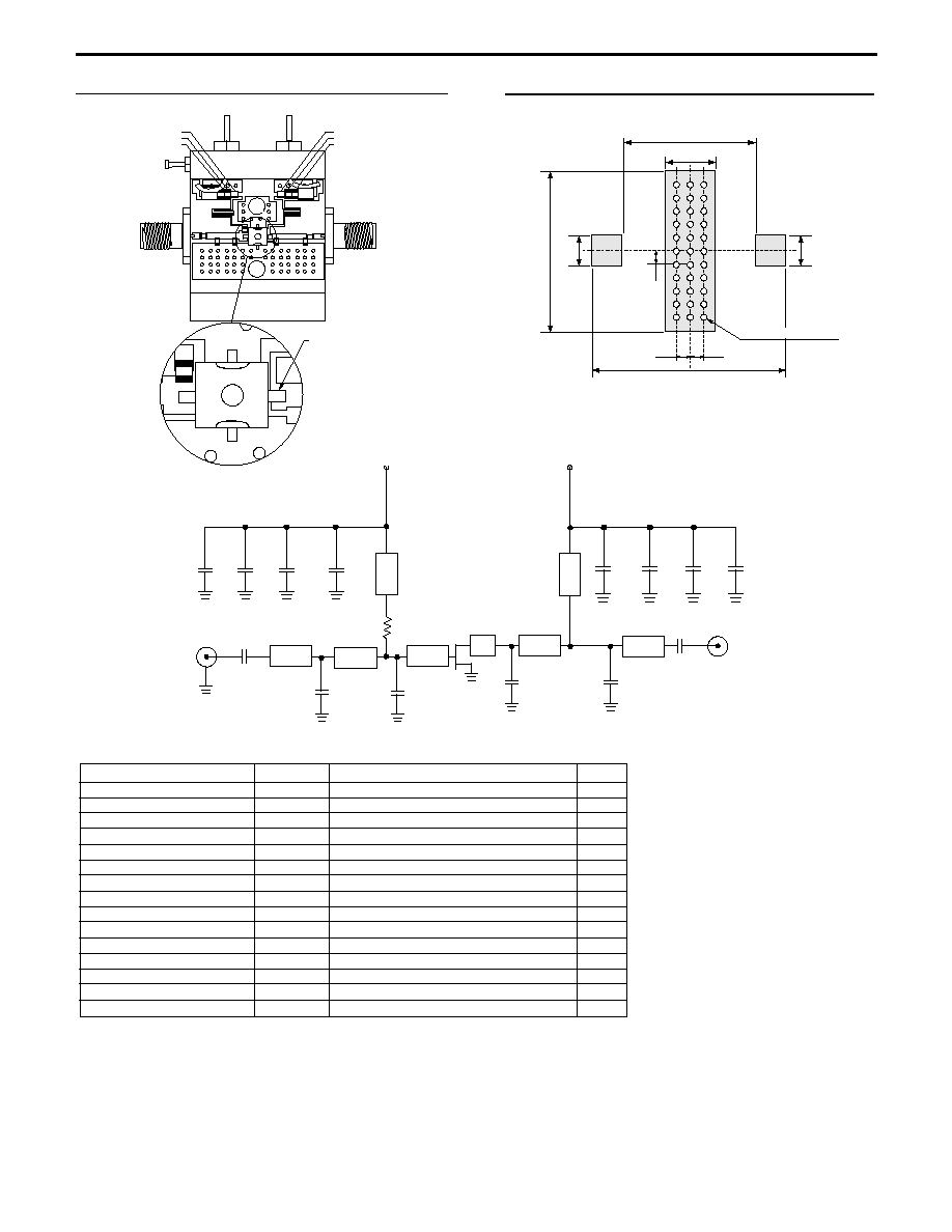
1 TF-100637
TEST CIRCUIT BLK
16
4
2-56 X 3/16 PHILLIPS PAN HEAD
15
2 MA101J
C2, C3
CASE 1100 pF CAP MURATA
14
1 MCR03J512
R1
0603 5.1K OHMS RESISTOR ROHM
13
2 MCH185A180JK
C4, C7
0603 18 pF CAP ROHM
12
1 MCH185A4R7CK
C14
0603 4.7 pF CAP ROHM
11
2 MCH185A100DK
C1, C5
0603 10 pF CAP ROHM
10
1 MCH185A8R2DK
C6
0603 8.2 pF CAP ROHM
9
2 TAJB475K010R
C12, C13 CASE B 4.7 uF CAP ATC
8
2 GRM40X7R104K025BL C10, C11
0805 .1 uF CAP MURATA
7
2 GRM40C0G102J050BD C8, C9
0805 1000 pF CAP MURATA 6
1 NE5520379A
U1
IC NEC, LD-MOS FET
5
1 703401
P1
GROUND LUG CONCORD
4
1 1250-003
J3, J4
FEEDTHRU MURATA
3
2 2052-5636-02
J1, J2
FLANGE MOUNT JACK RECEPTACLE
2
1 FD-100637
PCB
NE5520379A-EVAL FAB. DRAWING
1
NE5520379A PARTS LIST
V
GG
(+2.0 V)
RF Input
RF Output
100pF
NE5520379A
+
V
DD
(+3.1 V)
1000pF
4.7uF
0.1uF 4.7uF
100pF
1000pF
0.1uF
+
4.7pF
10pF
5K
18pF
18pF
8.2pF
10pF
J1
P1
GND
RF
IN
J2
RF
OUT
V
G
J3
V
D
J4
C3
C5
C9
C11
C2
C8
C10
R1
C1
C4
C14
U1
C6
100637
NE55XXX79A-EV
C12
C13
C7
LEAD ON DRAIN IS LARGER
DRAIN
GATE
SOURCE
A 3
A 3
APPLICATION CIRCUIT (900 MHz)
P.C.B. LAYOUT
(Units in mm)
79A PACKAGE
4.0
1.7
6.1
0.5
0.5
Source
Drain
Gate
5.9
1.2
1.0
0.5
Through hole 0.2 ◊ 33
Note:
Use rosin or other material to prevent solder from penetrating
through-holes.

Life Support Applications
These NEC products are not intended for use in life support devices, appliances, or systems where the malfunction of these products can reasonably
be expected to result in personal injury. The customers of CEL using or selling these products for use in such applications do so at their own risk and
agree to fully indemnify CEL for all damages resulting from such improper use or sale.
A Business Partner of NEC Compound Semiconductor Devices, Ltd.
03/08/2005
RECOMMENDED SOLDERING CONDITIONS
This prod
those recommended below, contact your nearby sales office.
NE5520379A
Soldering Method
Soldering Conditions
Condition Symbol
Infrared Reflow
Peak temperature (package surface temperature)
: 260∞C or below
Time at peak temperature
: 10 seconds or less
Time at temperature of 220∞C or higher
: 60 seconds or less
Preheating time at 120 to 180∞C
: 120±30 seconds
Maximum number of reflow processes
: 3 times
Maximum chlorine content of rosin flux (% mass)
: 0.2%(Wt.) or below
IR260
VPS
Peak temperature (package surface temperature)
: 215∞C or below
Time at temperature of 200∞C or higher
: 25 to 40 seconds
Preheating time at 120 to 150∞C
: 30 to 60 seconds
Maximum number of reflow processes
: 3 times
Maximum chlorine content of rosin flux (% mass)
: 0.2%(Wt.) or below
VP215
Wave Soldering
Peak temperature (molten solder temperature)
: 260∞C or below
Time at peak temperature
: 10 seconds or less
Preheating temperature (package surface temperature) : 120∞C or below
Maximum number of flow processes
: 1 time
Maximum chlorine content of rosin flux (% mass)
: 0.2%(Wt.) or below
WS260
Partial Heating
Peak temperature (pin temperature)
: 350∞C or below
Soldering time (per pin of device)
: 3 seconds or less
Maximum chlorine content of rosin flux (% mass)
: 0.2%(Wt.) or below
HS350-P3
Caution Do not use different soldering methods together (except for partial heating).

4590 Patrick Henry Drive
Santa Clara, CA 95054-1817
Telephone: (408) 919-2500
Facsimile: (408) 988-0279
Subject: Compliance with EU Directives
CEL certifies, to its knowledge, that semiconductor and laser products detailed below are compliant
with the requirements of European Union (EU) Directive 2002/95/EC Restriction on Use of Hazardous
Substances in electrical and electronic equipment (RoHS) and the requirements of EU Directive
2003/11/EC Restriction on Penta and Octa BDE.
CEL Pb-free products have the same base part number with a suffix added. The suffix ≠A indicates
that the device is Pb-free. The ≠AZ suffix is used to designate devices containing Pb which are
exempted from the requirement of RoHS directive (*). In all cases the devices have Pb-free terminals.
All devices with these suffixes meet the requirements of the RoHS directive.
This status is based on CEL's understanding of the EU Directives and knowledge of the materials that
go into its products as of the date of disclosure of this information.
Restricted Substance
per RoHS
Concentration Limit per RoHS
(values are not yet fixed)
Concentration contained
in CEL devices
-A
-AZ
Lead (Pb)
< 1000 PPM
Not Detected
(*)
Mercury
< 1000 PPM
Not Detected
Cadmium
< 100 PPM
Not Detected
Hexavalent Chromium
< 1000 PPM
Not Detected
PBB
< 1000 PPM
Not Detected
PBDE
< 1000 PPM
Not Detected
If you should have any additional questions regarding our devices and compliance to environmental
standards, please do not hesitate to contact your local representative.
Important Information and Disclaimer: Information provided by CEL on its website or in other communications concerting the substance
content of its products represents knowledge and belief as of the date that it is provided. CEL bases its knowledge and belief on information
provided by third parties and makes no representation or warranty as to the accuracy of such information. Efforts are underway to better
integrate information from third parties. CEL has taken and continues to take reasonable steps to provide representative and accurate
information but may not have conducted destructive testing or chemical analysis on incoming materials and chemicals. CEL and CEL
suppliers consider certain information to be proprietary, and thus CAS numbers and other limited information may not be available for
release.
In no event shall CEL's liability arising out of such information exceed the total purchase price of the CEL part(s) at issue sold by CEL to
customer on an annual basis.
See CEL Terms and Conditions for additional clarification of warranties and liability.