 | –≠–ª–µ–∫—Ç—Ä–æ–Ω–Ω—ã–π –∫–æ–º–ø–æ–Ω–µ–Ω—Ç: CDB42L50 | –°–∫–∞—á–∞—Ç—å:  PDF PDF  ZIP ZIP |

Preliminary Product Information
This document contains information for a new product.
Cirrus Logic reserves the right to modify this product without notice.
1
Copyright
„ Cirrus Logic, Inc. 2001
(All Rights Reserved)
P.O. Box 17847, Austin, Texas 78760
(512) 445 7222 FAX: (512) 445 7581
http://www.cirrus.com
Features
l
28-Pin CASON package
l
1.8 to 3.3 Volt supply
l
24-Bit conversion / 96 kHz sample rate
l
96 dB ADC/DAC dynamic range at 3 V supply
l
-88/-85 dB ADC/DAC THD+N
l
19 mW playback power consumption @ 1.8 V
l
Microphone or Line input amplifier with up to
32dB of gain
l
2:1 stereo mux
l
Digital volume control on inputs and outputs
≠ 96 dB attenuation, 1 dB step size
l
Digital bass and treble boost on outputs
≠ Selectable corner frequencies
l
Dynamic range compression and limiting
l
De-emphasis for 32 kHz, 44.1 kHz, and 48 kHz
l
Headphone amplifier
≠ 26 mW power output into 16 W load @ 3.0V
supply
≠ -80 dB THD+N
≠ 34 dB analog attenuation and mute
l
ATAPI mixing functions
Description
The CS42L50 is a highly integrated, 24-bit, 96 kHz audio
codec.
This device is based on delta-sigma modulation allowing
infinite adjustment of the sample rate between 8 kHz and
100 kHz simply by changing the master clock frequency.
The CS42L50 contains a 2:1 stereo mux, progra
mmable
analog gain control, and digital attenuation on the analog
inputs. The output D/A converters include digital bass
and treble boost, dynamic range compression, limiting,
mixing, volume control and de-emphasis.
The CS42L50 operates from a +1.8 V to +3.3 V supply.
These features are ideal for portable MP3 and MD re-
corders, CD and DVD recorders, digital camcorders, and
other portable systems that require extremely low power
consumption in a minimal amount of space.
ORDERING INFORMATION
CS42L50-KN 28-pin CASON, -10 to 70 ∞C
CDB42L50
Evaluation Board
I I
SCL
SDA
Control Port
Digital
Volume
Control
Bass/Treble
Boost
Compression
Limiting
Analog
Filter
Analog
Filter
HP_A
HP_B
AOUT_A
AOUT_B
RST
LRCK
SCLK
SDIN
S
e
ri
al
P
o
rt
De
-
e
m
p
h
a
s
i
s
Di
g
i
t
a
l
F
i
l
t
e
r
s
DAC
DAC
H
e
adp
ho
n
e
Am
p
l
i
f
i
e
r
Analog
Volume
Control
MCLK
Analog
Volume
Control
Line
A
m
p
lif
i
e
r
Co
mp
e
n
s
a
t
i
o
n
G
a
i
n
VA
VL
MUTEC
AIN_L1
AIN_L2
AIN_R1
AIN_R2
SDOUT
MUX
MUX
ADC
ADC
Digital
Filters
Attenuator
0-96 dB
Attenuator
0-96 dB
12 dB
Gain
Gain
12 dB
CS42L50
Low Voltage, Stereo CODEC with Headphone Amp
AUG `01
DS544PP1

CS42L50
2
DS544PP1
TABLE OF CONTENTS
1. CHARACTERISTICS/SPECIFICATIONS ................................................................................. 5
ANALOG INPUT CHARACTERISTICS .................................................................................... 5
ANALOG OUTPUT CHARACTERISTICS ................................................................................ 7
POWER AND THERMAL CHARACTERISTICS..................................................................... 10
DIGITAL CHARACTERISTICS ............................................................................................... 11
ABSOLUTE MAXIMUM RATINGS ......................................................................................... 11
RECOMMENDED OPERATING CONDITIONS ..................................................................... 11
SWITCHING CHARACTERISTICS ........................................................................................ 12
SWITCHING CHARACTERISTICS - CONTROL PORT......................................................... 14
2. TYPICAL CONNECTION DIAGRAM ....................................................................................... 15
3. REGISTER QUICK REFERENCE ........................................................................................... 16
4. REGISTER DESCRIPTION ..................................................................................................... 18
4.1 ADC (address 0010000) .................................................................................................. 18
4.1.1 I/O and Power Control (address 01h) .......................................................................... 18
4.1.2 20DB Gain Boost (BOOST) .......................................................................................... 18
4.1.3 Analog Input Multiplexer (AINMUX) ............................................................................... 18
4.1.4 Power Down (PDN)........................................................................................................ 18
4.1.5 Control Port Enable (CP_EN) ........................................................................................ 18
4.1.6 Interface Control (address 02h) .................................................................................... 19
4.1.7 Master Clock Divide (MCLKDIV)................................................................................... 19
4.1.8 Master Clock Ratio (RATIO) ......................................................................................... 19
4.1.9 Master Mode (MASTER)............................................................................................... 19
4.1.10 Digital Interface Format (DIF) ..................................................................................... 19
4.1.11 Analog I/O Control (address 03h) ............................................................................... 20
4.1.12 Left/Right Channel Mute (MUTE)............................................................................... 20
4.1.13 Soft Ramp and Zero Cross Enable (SOFT/ZC) ......................................................... 20
4.1.14 Independent Volume Control Enable (INDVC) .......................................................... 21
4.1.15 Left Channel Volume = Right Channel Volume (L=R) ............................................... 21
4.1.16 High-Pass Filter Freeze (HPFREEZE)....................................................................... 21
4.1.17 Volume Control: Left Channel (address 04h) & Right Channel (address 05h) ............ 22
4.1.18 Left/Right Analog Gain (address 06h) ........................................................................ 22
4.1.19 Clip Detection Status (address 07h) .......................................................................... 23
4.2 DAC (Address = 0010001) ............................................................................................... 23
4.2.1 Power and Muting Control (address 01h) .................................................................... 23
4.2.2 Auto-Mute (AMUTE) ..................................................................................................... 23
4.2.3 Soft Ramp and Zero Cross Control (SZC) ..................................................................... 23
4.2.4 Power Down Headphone Amplifier (PDNHP) ................................................................ 24
Contacting Cirrus Logic Support
For a complete listing of Direct Sales, Distributor, and Sales Representative contacts, visit the Cirrus Logic web site at:
http://www.cirrus.com/corporate/contacts/sales.cfm
Purchase of I
2
C components of Cirrus Logic, Inc., or one of its sublicensed Associated Companies conveys a license under the Philips I
2
C Patent Rights to use those
components in a standard I
2
C system.
Preliminary product information describes products which are in production, but for which full characterization data is not yet available. Advance product information de-
scribes products which are in development and subject to development changes. Cirrus Logic, Inc. has made best efforts to ensure that the information contained in this
document is accurate and reliable. However, the information is subject to change without notice and is provided "AS IS" without warranty of any kind (express or implied).
Customers are advised to obtain the latest version of relevant information to verify, before placing orders, that information being relied on is current and complete. All prod-
ucts are sold subject to the terms and conditions of sale supplied at the time of order acknowledgment, including those pertaining to warranty, patent infringement, and
limitation of liability. No responsibility is assumed by Cirrus Logic, Inc. for the use of this information, including use of this information as the basis for manufacture or sale
of any items, nor for infringements of patents or other rights of third parties. This document is the property of Cirrus Logic, Inc. and by furnishing this information, Cirrus
Logic, Inc. grants no license, express or implied under any patents, mask work rights, copyrights, trademarks, trade secrets or other intellectual property rights of Cirrus
Logic, Inc. Cirrus Logic, Inc., copyright owner of the information contained herein, gives consent for copies to be made of the information only for use within your organization
with respect to Cirrus Logic integrated circuits or other parts of Cirrus Logic, Inc. The same consent is given for similar information contained on any Cirrus Logic website
or disk. This consent does not extend to other copying such as copying for general distribution, advertising or promotional purposes, or for creating any work for resale.
The names of products of Cirrus Logic, Inc. or other vendors and suppliers appearing in this document may be trademarks or service marks of their respective owners which
may be registered in some jurisdictions. A list of Cirrus Logic, Inc. trademarks and service marks can be found
at
http://www.cirrus.com
.

CS42L50
DS544PP1
3
4.2.5 Power Down Line Amplifier (PDNLN)............................................................................ 24
4.2.6 Power Down (PDN) ....................................................................................................... 24
4.2.7 Control Port Enable (CP_EN)........................................................................................ 24
4.2.8 Channel A Analog Headphone Attenuation Control (address 02h) (HVOLA) .............. 25
4.2.9 Channel B Analog Headphone Attenuation Control (address 03h) (HVOLB) .............. 25
4.2.10 Channel A Digital Volume Control (address 04h) (DVOLA) ....................................... 25
4.2.11 Channel B Digital Volume Control (address 05h) (DVOLB) ....................................... 25
4.2.12 Tone Control (address 06h)........................................................................................ 26
4.2.13 Bass Boost Level (BB)................................................................................................. 26
4.2.14 Treble Boost Level (TB)............................................................................................... 26
4.2.15 Mode Control (address 07h)....................................................................................... 27
4.2.16 Bass Boost Corner Frequency (BBCF) ....................................................................... 27
4.2.17 Treble Boost Corner Frequency (TBCF) ..................................................................... 27
4.2.18 Channel A Volume = Channel B Volume (A=B) .......................................................... 27
4.2.19 De-Emphasis Control (DEM) ....................................................................................... 28
4.2.20 Digital Volume Control Bypass (VCBYP) .................................................................... 28
4.2.21 Volume and Mixing Control (address 0Ah)................................................................. 28
4.2.22 Tone Control Mode (TC).............................................................................................. 28
4.2.23 Tone Control Enable (TC_EN) .................................................................................... 28
4.2.24 ATAPI Channel Mixing and Muting (ATAPI)................................................................ 29
4.2.25 Mode Control 2 (address 0Bh) ................................................................................... 29
4.2.26 Master Clock Divide Enable (MCLKDIV) ..................................................................... 29
4.2.27 Line Amplifier Gain Compensation (LINE)................................................................... 29
4.2.28 Digital Interface Format (DIF) ...................................................................................... 30
5. PIN DESCRIPTIONS ............................................................................................................... 31
6. APPLICATIONS ...................................................................................................................... 33
6.1 Grounding and Power Supply Decoupling ....................................................................... 33
6.2 Clock Modes .................................................................................................................... 33
6.3 EP73xx Serial Port Interface ........................................................................................... 33
6.4 De-Emphasis ................................................................................................................... 33
6.5 Recommended Power-up Sequence ............................................................................... 33
6.6 Optional External Headphone Mute ................................................................................ 33
7. CONTROL PORT INTERFACE ............................................................................................... 33
7.1 Memory Address Pointer (MAP) ...................................................................................... 35
7.2 INCR (Auto Map Increment Enable)................................................................................. 35
7.3 MAP0-3 (Memory Address Pointer).................................................................................. 35
8. PARAMETER DEFINITIONS ................................................................................................... 44
9. REFERENCES ......................................................................................................................... 44
10. PACKAGE DIMENSIONS ..................................................................................................... 45
LIST OF FIGURES
Figure 1. SCLK to LRCK and SDIN, Slave Mode .................................................... 13
Figure 2. SCLK to LRCK and SDIN, Master Mode .................................................. 13
Figure 3. Control Port Timing - I
2
C, ......................................................................... 14
Figure 4. CS42L50 Typical Connection Diagram .................................................... 15
Figure 5. Control Port Timing .................................................................................. 35
Figure 6. Decimation Filter Single Speed Stopband Rejection ............................... 36
Figure 7. Decimation Filter Single Speed Transition Band ...................................... 36
Figure 8. Decimation Filter Single Speed Transition Band (Detail) ......................... 36
Figure 9. Decimation Filter Single Speed Passband Ripple ................................... 36
Figure 10.Decimation Filter Double Speed Stopband Rejection .............................. 36
Figure 11.Decimation Filter Double Speed Transition Band .................................... 36
Figure 12.Decimation Filter Double Speed Transition Band (Detail) ........................ 37

CS42L50
4
DS544PP1
Figure 13.Decimation Filter Double Speed Passband Ripple .................................. 37
Figure 14.Interpolation Filter Single Speed Stopband Rejection .............................. 38
Figure 15.Interpolation Filter Single Speed Transition Band .................................... 38
Figure 16.Interpolation Filter Single Speed Transition Band (Detail) ....................... 38
Figure 17.Interpolation Filter Single Speed Passband Ripple .................................. 38
Figure 18.Interpolation Filter Double Speed Stopband Rejection ............................ 38
Figure 19.Interpolation Filter Double Speed Transition Band ................................... 38
Figure 20.Interpolation Filter Double Speed Transition Band (Detail) ...................... 39
Figure 21.Interpolation Filter Double Speed Passband Ripple ................................. 39
Figure 22.Line Input Test Circuit .............................................................................. 39
Figure 23.Line Output Test Load .............................................................................. 40
Figure 24.Headphone Output Test Load .................................................................. 40
Figure 25.Left Justified, up to 24-bit data ................................................................. 41
Figure 26.Right Justified, 16-bit data ........................................................................ 41
Figure 27.Right Justified, 24-bit data ........................................................................ 41
Figure 28.Right Justified, 18-bit data ........................................................................ 42
Figure 29.Right Justified, 20-bit data ........................................................................ 42
Figure 30.I2S, up to 24-bit data ................................................................................ 42
Figure 31.De-Emphasis Curve ................................................................................. 43
Figure 32.ATAPI Block Diagram ............................................................................... 43
Figure 33.Package Dimensions ................................................................................ 45
Figure 34.Package Top and Side Views .................................................................. 46
Figure 35.Package Bottom View .............................................................................. 47
LIST OF TABLES
Table 1. Example Analog Volume Settings ...................................................................................25
Table 2. Example Digital Volume Settings ....................................................................................26
Table 3. Example Bass Boost Settings .........................................................................................26
Table 4. Example Treble Boost Settings .......................................................................................27
Table 5. ATAPI Decode.................................................................................................................29
Table 6. Digital Interface Format ...................................................................................................30
CS42L50
DS544PP1
5
1.
CHARACTERISTICS/SPECIFICATIONS
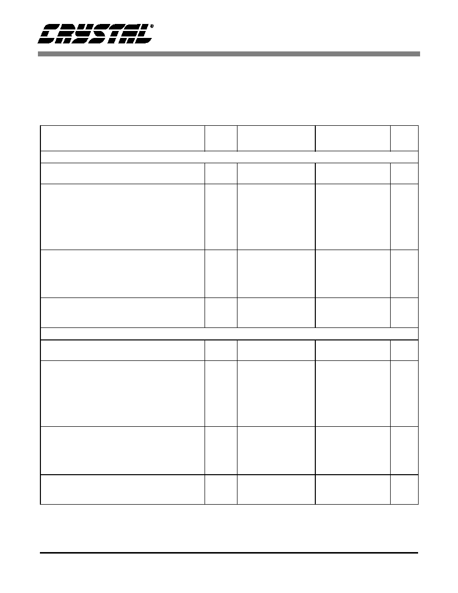
ANALOG INPUT CHARACTERISTICS
(T
A
= 25∞ C; GND = 0 V Logic "1" = VL = 1.8 V; Logic "0" =
GND = 0 V; MCLK = 12.288 MHz; Fs for Single Speed Mode = 48 kHz, SCLK = 3.072 MHz, Fs for Double Speed
Mode = 96 kHz, SCLK = 6.144 MHz; Measurement Bandwidth 10 Hz to 20 kHz, unless otherwise specified. Input is
997Hz sine wave.)
Parameter
Symbol
Single Speed Mode Double Speed Mode
Unit
Min
Typ
Max
Min
Typ
Max
Analog Input Characteristics for VA = 1.8 V
Dynamic Range
A-weighted
unweighted
TBD
TBD
93
90
-
-
TBD
TBD
94
91
-
-
dB
dB
Total Harmonic Distortion + Noise
(Note 1)
18 to 24-Bit
-1 dB
-20 dB
-60 dB
16-Bit
-1 dB
-20 dB
-60 dB
THD+N
-
-
-
-
-
-
-88
-70
-30
-86
-68
-28
TBD
-
-
-
-
-
-
-
-
-
-
-
-88
-71
-31
-86
-68
-28
TBD
-
-
-
-
-
dB
dB
dB
dB
dB
dB
Dynamic Range (PGA on)*
0 dB Gain A-weighted
unweighted
12 dB Gain A-weighted
unweighted
-
-
-
-
90
87
85
82
-
-
-
-
-
-
-
-
89
86
86
83
-
-
-
-
dB
dB
dB
dB
Total Harmonic Distortion + Noise (PGA on)*
(Note 1)
0 dB Gain, 18 to 24-Bit -1 dB
12 dB Gain, 18 to 24-Bit -1 dB
THD+N
-
-
85
83
-
-
-
-
84
82
-
-
dB
dB
Analog Input Characteristics for VA = 3.0 V
Dynamic Range
A-weighted
unweighted
TBD
TBD
96
93
-
-
TBD
TBD
98
95
-
-
dB
dB
Total Harmonic Distortion + Noise
(Note 1)
18 to 24-Bit
-1 dB
-20 dB
-60 dB
16-Bit
-1 dB
-20 dB
-60 dB
THD+N
-
-
-
-
-
-
-88
-73
-33
-86
-68
-28
TBD
-
-
-
-
-
-
-
-
-
-
-
-85
-75
-35
-83
-65
-28
TBD
-
-
-
-
-
dB
dB
dB
dB
dB
dB
Dynamic Range (PGA on)*
0 dB Gain A-weighted
unweighted
12 dB Gain A-weighted
unweighted
-
-
-
-
93
90
88
85
-
-
-
-
-
-
-
-
92
89
89
86
-
-
-
-
dB
dB
dB
dB
Total Harmonic Distortion + Noise (PGA on)*
(Note 1)
0 dB Gain, 18 to 24-Bit -1 dB
12 dB Gain, 18 to 24-Bit -1 dB
THD+N
-
-
78
73
-
-
-
-
77
76
-
-
dB
dB
*PGA : Programmable Gain Amplifier