 | –≠–ª–µ–∫—Ç—Ä–æ–Ω–Ω—ã–π –∫–æ–º–ø–æ–Ω–µ–Ω—Ç: CDB8427 | –°–∫–∞—á–∞—Ç—å:  PDF PDF  ZIP ZIP |
1
Copyright
©
Cirrus Logic, Inc. 2005
(All Rights Reserved)
www.cirrus.com
CS8427
96 kHz Digital Audio Interface Transceiver
Features
Complete EIAJ CP1201, IEC-60958, AES3,
S/PDIF-compatible Transceiver
+5.0 V Analog Supply (VA+)
+3.3 V or +5.0 V Digital Interface (VL+)
Flexible 3-wire Serial Digital I/O Ports
Adjustable Sample Rate up to 96 kHz
Low-jitter Clock Recovery
Pin and Microcontroller Read/Write Access to
Channel Status and User Data
Microcontroller and Standalone Modes
Differential Cable Driver and Receiver
On-chip Channel Status and User Data Buffer
Memories Permit Block Reads & Writes
OMCK System Clock Mode
Decodes Audio CD Q Sub-code
General Description
The CS8427 is a stereo digital audio transceiver with
AES3 and serial digital audio inputs, AES3 and serial
digital audio outputs, and includes comprehensive con-
trol ability through a 4-wire microcontroller port. Channel
status and user data are assembled in block-sized buff-
ers, making read/modify/write cycles easy.
A low-jitter clock recovery mechanism yields a very clean
recovered clock from the incoming AES3 stream.
Target applications include A/V receivers, CD-R, DVD
receivers, multimedia speakers, digital mixing consoles,
effects processors, set-top boxes, and computer and au-
tomotive audio systems.
ORDERING INFORMATION
CS8427-CS
28-pin SOIC -10 to +70∞C
CS8427-CSZ, Lead Free 28-pin SOIC -10 to +70∞C
CS8427-CZ
28-pin TSSOP -10 to +70∞C
CS8427-DS
28-pin SOIC -40 to +85∞C
CS8427-DZ
28-pin TSSOP -40 to +85∞C
CDB8427
Evaluation Board
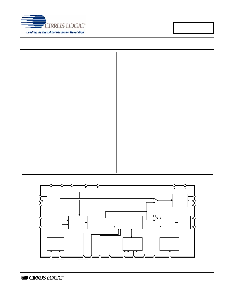
I
Serial
Audio
Input
Clock &
Data
Recovery
Misc.
Control
AES3
S/PDIF
Encoder
Serial
Audio
Output
Receiver
AES3
S/PDIF
Decoder
C & U bit
Data
Buffer
Control
Port &
Registers
Output
Clock
Generator
RXN
RXP
ILRCK
ISCLK
SDIN
OLRCK
OSCLK
SDOUT
TXP
TXN
RST
OMCK
EMPH U TCBL SDA/
CDOUT
SCL/
CCLK
AD1/
CDIN
AD0/
CS
INT
VA+ AGND FILT
RERR
VL+ DGND
H/S
RMCK
Driver
JAN `05
DS477F3

CS8427
2
DS477F3
TABLE OF CONTENTS
1. CHARACTERISTICS AND SPECIFICATIONS ........................................................................ 5
Specified Operating Conditions ................................................................................................ 5
Absolute Maximum Ratings ...................................................................................................... 5
DC Electrical Characteristics .................................................................................................... 6
Digital Input Characteristics ...................................................................................................... 6
Digital Interface Specifications................................................................................................ 6
Transmitter Characteristics ....................................................................................................... 6
Switching Characteristics.......................................................................................................... 7
Switching Characteristics - Serial Audio Ports.......................................................................... 8
Switching Characteristics - Control Port - SPI Mode ................................................................ 9
Switching Characteristics - Control Port - I≤C Mode ............................................................... 10
2. TYPICAL CONNECTION DIAGRAM ...................................................................................... 11
3. GENERAL DESCRIPTION ..................................................................................................... 12
3.1 Audio Input/Output Ports ................................................................................................. 12
3.2 Serial Control Port ............................................................................................................ 12
3.3 Channel Status and User bit Memory .............................................................................. 12
3.4 AES3 and S/PDIF Standards Documents ........................................................................ 13
4. DATA I/O FLOW AND CLOCKING OPTIONS ....................................................................... 13
5. THREE-WIRE SERIAL AUDIO PORTS ................................................................................. 15
6. AES3 RECEIVER .................................................................................................................... 16
6.1 OMCK System Clock Mode ............................................................................................. 16
6.2 PLL, Jitter Attenuation, and Varispeed ............................................................................ 16
6.3 Error Reporting and Hold Function .................................................................................. 16
6.4 Channel Status Data Handling ......................................................................................... 16
6.5 User Data Handling .......................................................................................................... 17
6.6 Non-Audio Auto Detection ............................................................................................... 17
7. AES3 TRANSMITTER ........................................................................................................... 18
7.1 Transmitted Frame and Channel Status Boundary Timing .............................................. 18
7.2 TXN and TXP Drivers ...................................................................................................... 18
8. MONO MODE OPERATION ................................................................................................... 19
8.1 Receiver Mono Mode ....................................................................................................... 19
8.2 Transmitter Mono Mode ................................................................................................... 19
9. CONTROL PORT DESCRIPTION AND TIMING .................................................................... 25
9.1 SPITM Mode .................................................................................................................... 25
9.2 I≤C Mode .......................................................................................................................... 25
9.3 Interrupts .......................................................................................................................... 25
10. CONTROL PORT REGISTER SUMMARY ........................................................................... 27
10.1 Memory Address Pointer (MAP) ..................................................................................... 27
11. CONTROL PORT REGISTER BIT DEFINITIONS ................................................................ 28
11.1 Control 1 (01h) ................................................................................................................ 28
11.2 Control 2 (02h) ................................................................................................................ 28
11.3 Data Flow Control (03h).................................................................................................. 29
11.4 Clock Source Control (04h)............................................................................................. 30
11.5 Serial Audio Input Port Data Format (05h)...................................................................... 31
11.6 Serial Audio Output Port Data Format (06h)................................................................... 31
11.7 Interrupt 1 Status (07h) (Read Only)............................................................................... 32
11.8 Interrupt 2 Status (08h) (Read Only)............................................................................... 33
11.9 Interrupt 1 Mask (09h)..................................................................................................... 33
11.10 Interrupt 1 Mode MSB (0Ah) & Interrupt 1 Mode LSB (0Bh)......................................... 33
11.11 Interrupt 2 Mask (0Ch) .................................................................................................. 34
11.12 Interrupt 2 Mode MSB (0Dh) & Interrupt 2 Mode LSB (0Eh) ........................................ 34
11.13 Receiver Channel Status (0Fh) (Read Only) ................................................................ 34

CS8427
DS477F3
3
11.14 Receiver Error (10h) (Read Only)................................................................................. 35
11.15 Receiver Error Mask (11h) ........................................................................................... 36
11.16 Channel Status Data Buffer Control (12h).................................................................... 36
11.17 User Data Buffer Control (13h)..................................................................................... 37
11.18 Q-Channel Subcode Bytes 0 to 9 (14h - 1Dh) (Read Only) ......................................... 37
11.19 OMCK/RMCK Ratio (1Eh) (Read Only)........................................................................ 38
11.20 C-bit or U-bit Data Buffer (20h - 37h) ........................................................................... 38
11.21 CS8427 I.D. and Version Register (7Fh) (Read Only) ................................................. 38
12. PIN DESCRIPTION - SOFTWARE MODE ........................................................................... 39
13. HARDWARE MODE DESCRIPTION ................................................................................... 42
13.1 Serial Audio Port Formats ............................................................................................. 42
14. PIN DESCRIPTION - HARDWARE MODE .......................................................................... 44
15. APPLICATIONS ................................................................................................................... 46
15.1 Reset, Power Down and Start-up .................................................................................. 46
15.2 ID Code and Revision Code .......................................................................................... 46
15.3 Power Supply, Grounding, and PCB layout ................................................................... 46
15.4 Synchronization of Multiple CS8427s ............................................................................ 46
16. PACKAGE DIMENSIONS .................................................................................................... 47
17. APPENDIX A: EXTERNAL AES3/SPDIF/IEC60958 TRANSMITTER AND RECEIVER COMPO-
NENTS .................................................................................................................................. 49
17.1 AES3 Transmitter External Components ....................................................................... 49
17.2 Isolating Transformer Requirements ............................................................................. 49
17.3 AES3 Receiver External Components ........................................................................... 50
17.4 Isolating Transformer Requirements ............................................................................. 50
18. APPENDIX B: CHANNEL STATUS AND USER DATA BUFFER MANAGEMENT ........... 51
18.1 AES3 Channel Status(C) Bit Management .................................................................... 51
18.1.1 Manually accessing the E buffer ....................................................................... 51
18.1.2 Reserving the first 5 bytes in the E buffer ......................................................... 52
18.1.3 Serial Copy Management System (SCMS) ....................................................... 52
18.1.4 Channel Status Data E Buffer Access .............................................................. 52
18.2 AES3 User (U) Bit Management .................................................................................... 53
18.2.1 Mode 1: Transmit All Zeros ............................................................................... 53
18.2.2 Mode 2: Block Mode ......................................................................................... 53
19. APPENDIX C: PLL FILTER .................................................................................................. 54
19.1 General .......................................................................................................................... 54
19.2 External Filter Components ........................................................................................... 55
19.2.1 General ............................................................................................................. 55
19.2.2 Capacitor Selection ........................................................................................... 55
19.2.3 Circuit Board Layout ......................................................................................... 55
19.3 Component Value Selection .......................................................................................... 56
19.3.1 Identifying the Part Revision ............................................................................. 56
19.3.2 Locking to the RXP/RXN Receiver Inputs ......................................................... 56
19.3.3 Locking to the ILRCK Input ............................................................................... 57
19.3.4 Jitter Tolerance ................................................................................................. 57
19.3.5 Jitter Attenuation ............................................................................................... 58
20. REVISION HISTORY ............................................................................................................ 59

CS8427
4
DS477F3
LIST OF FIGURES
Figure 1. Audio Port Master Mode Timing....................................................................................... 8
Figure 2. Audio Port Slave Mode and Data Input Timing ................................................................ 8
Figure 3. SPI Mode timing............................................................................................................... 9
Figure 4. I≤C Mode timing.............................................................................................................. 10
Figure 5. Recommended Connection Diagram for Software Mode............................................... 11
Figure 6. CS8427 Internal Block Diagram..................................................................................... 13
Figure 7. Software Mode Audio Data Flow Switching Options...................................................... 19
Figure 8. CS8427 Clock Routing................................................................................................... 20
Figure 9. AES3 Input to Serial Audio Output, Serial Audio Input to AES3 Out ............................. 21
Figure 11. Input Serial Port to AES3 Transmitter without PLL ...................................................... 21
Figure 10. AES3 Input to Serial Audio Output Only ...................................................................... 21
Figure 12. Input Serial Port to AES3 Transmitter with PLL ........................................................... 21
Figure 13. AES3 Receiver Timing for U pin output data ............................................................... 22
Figure 14. AES3 Transmitter Timing for C, U and V pin input data............................................... 22
Figure 15. Serial Audio Input Example Formats............................................................................ 23
Figure 16. Serial Audio Output Example Formats......................................................................... 24
Figure 17. Control Port Timing in SPI Mode.................................................................................. 26
Figure 18. Control Port Timing in I≤C Mode................................................................................... 26
Figure 19. Hardware Mode............................................................................................................ 42
Figure 20. Professional Output Circuit .......................................................................................... 49
Figure 21. Consumer Output Circuit.............................................................................................. 49
Figure 22. TTL/CMOS Output Circuit ............................................................................................ 49
Figure 23. Professional Input Circuit ............................................................................................. 50
Figure 24. Transformerless Professional Input Circuit .................................................................. 50
Figure 25. Consumer Input Circuit ................................................................................................ 50
Figure 26. TTL/CMOS Input Circuit............................................................................................... 50
Figure 27. Channel Status Data Buffer Structure.......................................................................... 51
Figure 28. Flowchart for Reading the E Buffer .............................................................................. 52
Figure 29. Flowchart for Writing the E Buffer ................................................................................ 52
Figure 30. PLL Block Diagram ...................................................................................................... 54
Figure 31. Recommended Layout Example .................................................................................. 55
Figure 32. Jitter Tolerance Template ............................................................................................ 57
Figure 33. Revision A .................................................................................................................... 58
Figure 34. Revision A1 .................................................................................................................. 58
Figure 35. Revision A2 using A1 values........................................................................................ 58
Figure 36. Revision A2 using A2* values ...................................................................................... 58
LIST OF TABLES
Table 1. Control Register Map Summary ...................................................................................... 27
Table 2. Hardware Mode Start-up Options.................................................................................... 43
Table 3. Serial Audio Output Formats Available in Hardware Mode ............................................. 43
Table 4. Serial Audio Input Formats Available in Hardware Mode................................................ 43
Table 5. Second Line Part Marking ............................................................................................... 56
Table 6. Locking to RXP/RXN - Fs = 8 to 96 kHz ......................................................................... 56
Table 7. Locking to RXP/RXN - Fs = 32 to 96 kHz ....................................................................... 56
Table 8. Locking to the ILRCK Input ............................................................................................. 57
Table 9. Revision History .............................................................................................................. 59
CS8427
DS477F3
5
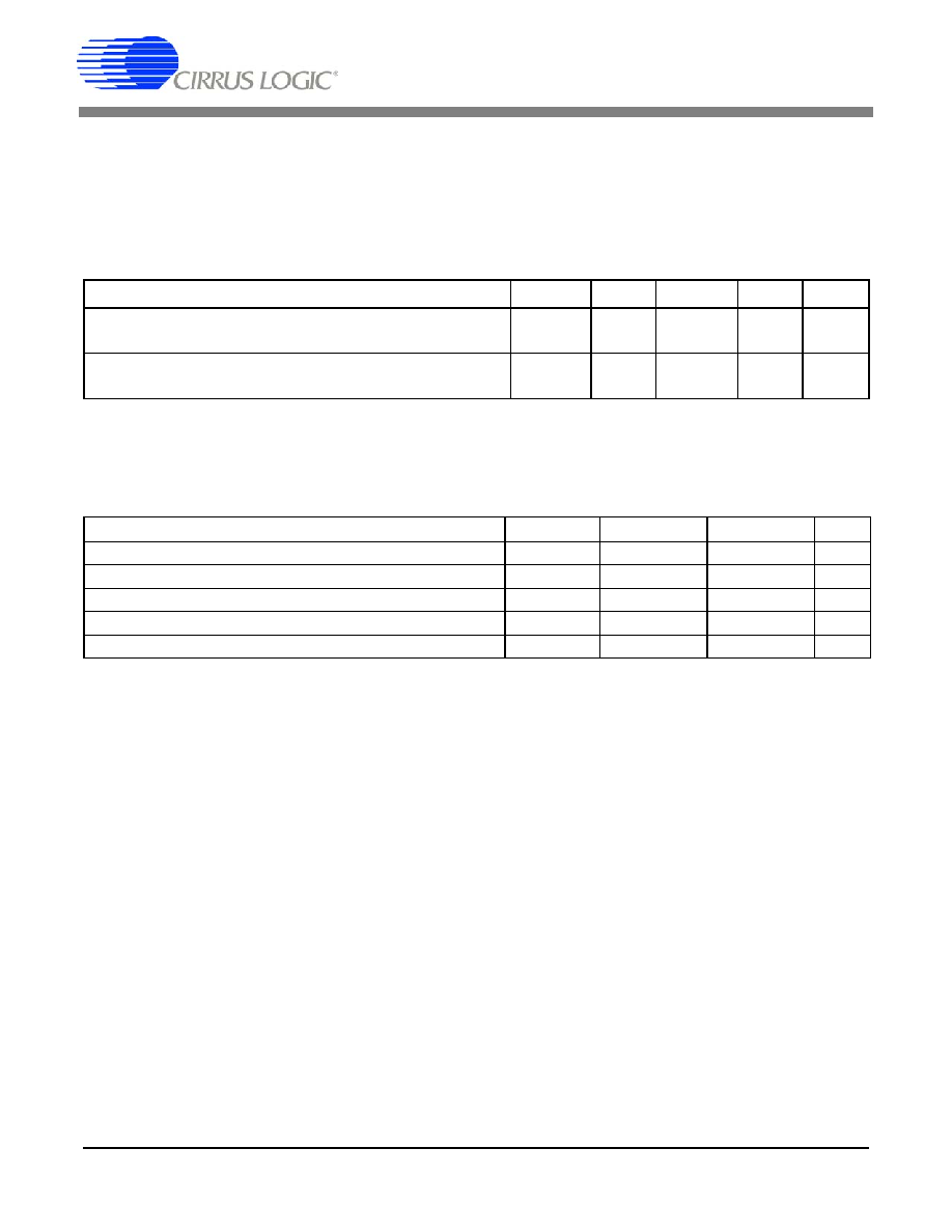
1. CHARACTERISTICS AND SPECIFICATIONS
All Min/Max characteristics and specifications are guaranteed over the Specified Operating Conditions. Typical per-
formance characteristics and specifications are derived from measurements taken at nominal supply voltages and
T
A
= 25∞C.
SPECIFIED OPERATING CONDITIONS
AGND, DGND = 0 V, all voltages with respect to 0 V.
Notes: 1. I≤C protocol is supported only in VL+ = 5.0 V mode.
ABSOLUTE MAXIMUM RATINGS
AGND, DGND = 0 V; all voltages with respect to 0 V. Operation beyond these limits may result in permanent dam-
age to the device. Normal operation is not guaranteed at these extremes.
Notes: 2. Transient currents of up to 100 mA will not cause SCR latch-up.
Parameter
Symbol Min Typ
Max
Units
Power Supply Voltage
(Note 1)
VA+
VL+
4.5
2.85
5.0
3.3 or 5.0
5.5
5.5
V
V
Ambient Operating Temperature:
`-CS', `CSZ' & `-CZ'
`-DS' & `-DZ'
T
A
-10
-40
-
-
+70
+85
∞C
Parameter
Symbol
Min
Max
Units
Power Supply Voltage
VL+,VA+
-
6.0
V
Input Current, Any Pin Except Supplies
(Note 2)
I
in
-
±10
mA
Input Voltage
V
in
-0.3
(VL+) + 0.3
V
Ambient Operating Temperature (power applied)
T
A
-55
125
∞C
Storage Temperature
T
stg
-65
150
∞C
CS8427
6
DS477F3
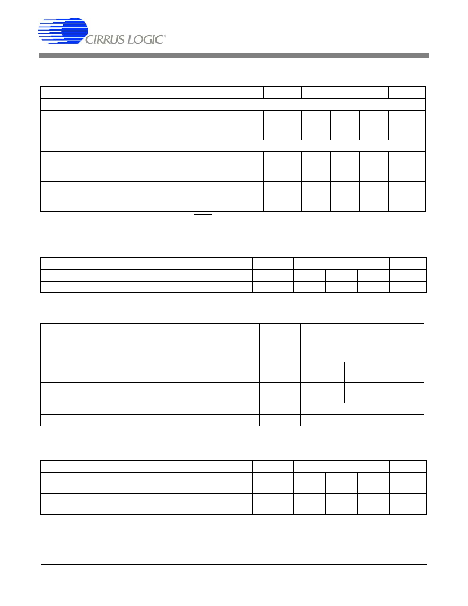
DC ELECTRICAL CHARACTERISTICS
AGND = DGND = 0 V; all voltages with respect to 0 V.
Notes: 3. Power Down Mode is defined as RST = LO with all clocks and data lines held static.
4. Normal operation is defined as RST = HI.
DIGITAL INPUT CHARACTERISTICS
DIGITAL INTERFACE SPECIFICATIONS
AGND = DGND = 0 V; all voltages with respect to 0 V.
Notes: 5. At 5.0 V mode, V
IL
= 0.8 V (Max), at 3.3 V mode, V
IL
=0.4 V (Max).
TRANSMITTER CHARACTERISTICS
Parameters
Symbol
Min
Typ
Max
Units
Power-down Mode
(Note 3)
Supply Current in power down
VA+
VL+ = 3.3 V
VL+ = 5.0 V
-
-
-
20
60
60
-
-
-
µ
A
µ
A
µ
A
Normal Operation
(Note 4)
Supply Current at 48 kHz frame rate
VA+
VL+ = 3.3 V
VL+ = 5.0 V
-
-
-
6.3
30.1
46.5
-
-
-
mA
mA
mA
Supply Current at 96 kHz frame rate
VA+
VL+ = 3.3 V
VL+ = 5.0 V
-
-
-
6.6
44.8
76.6
-
-
-
mA
mA
mA
Parameters
Symbol Min Typ
Max
Units
Input Leakage Current
I
in
-
±1
±10
µ
A
Differential Input Voltage, RXP0 to RXN
V
TH
-
200
-
mV
Parameters
Symbol Min Max
Units
High-Level Output Voltage (I
OH
= -3.2 mA), except TXP/TXN
V
OH
(VL+) - 1.0
-
V
Low-Level Output Voltage (I
OH
= 3.2 mA), except TXP/TXN
V
OL
-
0.4
V
High-Level Output Voltage, TXP, TXN
(23 mA at VL+ = 5.0 V)
(15.2 mA at VL+ = 3.3 V)
(VL+) - 0.7
(VL+) - 0.7
-
-
V
V
Low-Level Output Voltage, TXP, TXN
(23 mA at VL+ = 5.0 V)
(15.2 mA at VL+ = 3.3 V)
-
-
0.7
0.7
V
V
High-Level Input Voltage, except RXP, RXN
V
IH
2.0
(VL+) + 0.3
V
Low-Level Input Voltage, except RXP, RXN
(Note 5)
V
IL
-0.3
0.4/0.8
V
Parameters
Symbol Min Typ
Max
Units
TXP Output Resistance
VL+ = 5.0 V
VL+ = 3.3 V
R
TXP
-
-
26
40
-
-
TXN Output Resistance
VL+ = 5.0 V
VL+ = 3.3 V
R
TXN
-
-
26
40
-
-

CS8427
DS477F3
7
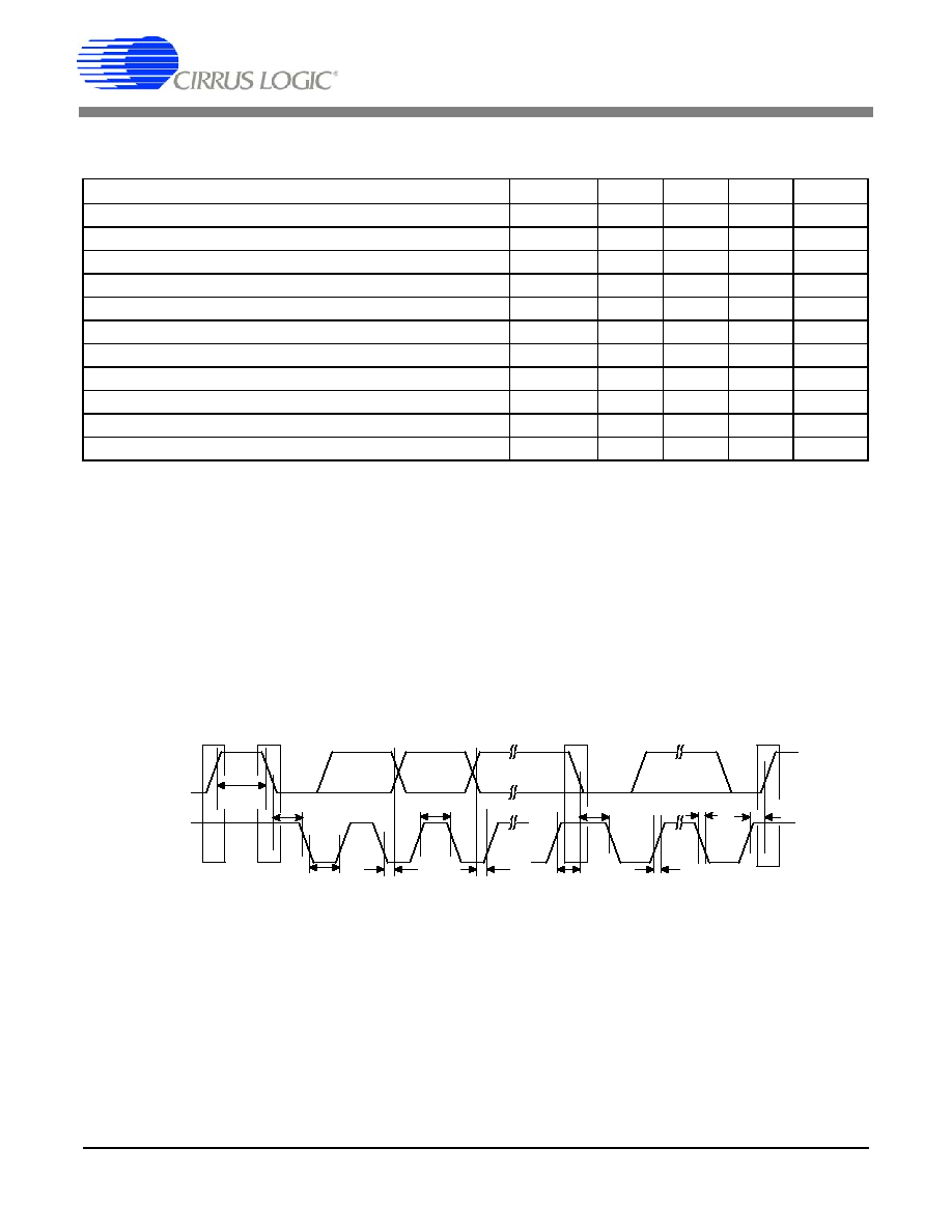
SWITCHING CHARACTERISTICS
Inputs: Logic 0 = 0 V, Logic 1 = VL+; C
L
= 20 pF.
Notes: 6. Cycle-to-cycle locking to RXP/RXN using 32 to 96 kHz external PLL filter components.
7. PLL is bypassed (RXD1:0 bits in the Clock Source Control register set to 10b), clock is input to the
RMCK pin.
Parameter
Symbol Min Typ
Max
Units
RST pin Low Pulse Width
200
-
-
µ
s
OMCK Frequency for OMCK = 512 * Fso
4.1
-
55.3
MHz
OMCK Low and High Width for OMCK = 512 * Fso
7.2
-
-
ns
OMCK Frequency for OMCK = 384 * Fso
3.1
-
41.5
MHz
OMCK Low and High Width for OMCK = 384 * Fso
10.8
-
-
ns
OMCK Frequency for OMCK = 256 * Fso
2.0
-
27.7
MHz
OMCK Low and High Width for OMCK = 256 * Fso
14.4
-
-
ns
PLL Clock Recovery Sample Rate Range
8.0
-
108.0
kHz
RMCK output jitter
(Note 6)
-
200
-
ps RMS
RMCK output duty cycle
40
50
60
%
RMCK Input Frequency
(Note 7)
1.8
-
27.7
MHz
RMCK Input Low and High Width
(Note 7)
14.4
-
-
ns
AES3 Transmitter Output Jitter
-
-
1
ns

CS8427
8
DS477F3
SWITCHING CHARACTERISTICS - SERIAL AUDIO PORTS
Inputs: Logic 0 = 0 V, Logic 1 = VL+; C
L
= 20 pF.
Notes: 8. The active edges of ISCLK and OSCLK are programmable.
9. When OSCLK, OLRCK, ISCLK, and ILRCK are derived from OMCK they are clocked from its rising
edge. When these signals are derived from RMCK, they are clocked from its falling edge.
10. The polarity of ILRCK and OLRCK is programmable.
11. No more than 128 SCLK per frame.
12. This delay is to prevent the previous I/OSCLK edge from being interpreted as the first one after I/OLRCK
has changed.
13. This setup time ensures that this I/OSCLK edge is interpreted as the first one after I/OLRCK has
changed.
Parameter
Symbol Min Typ
Max
Units
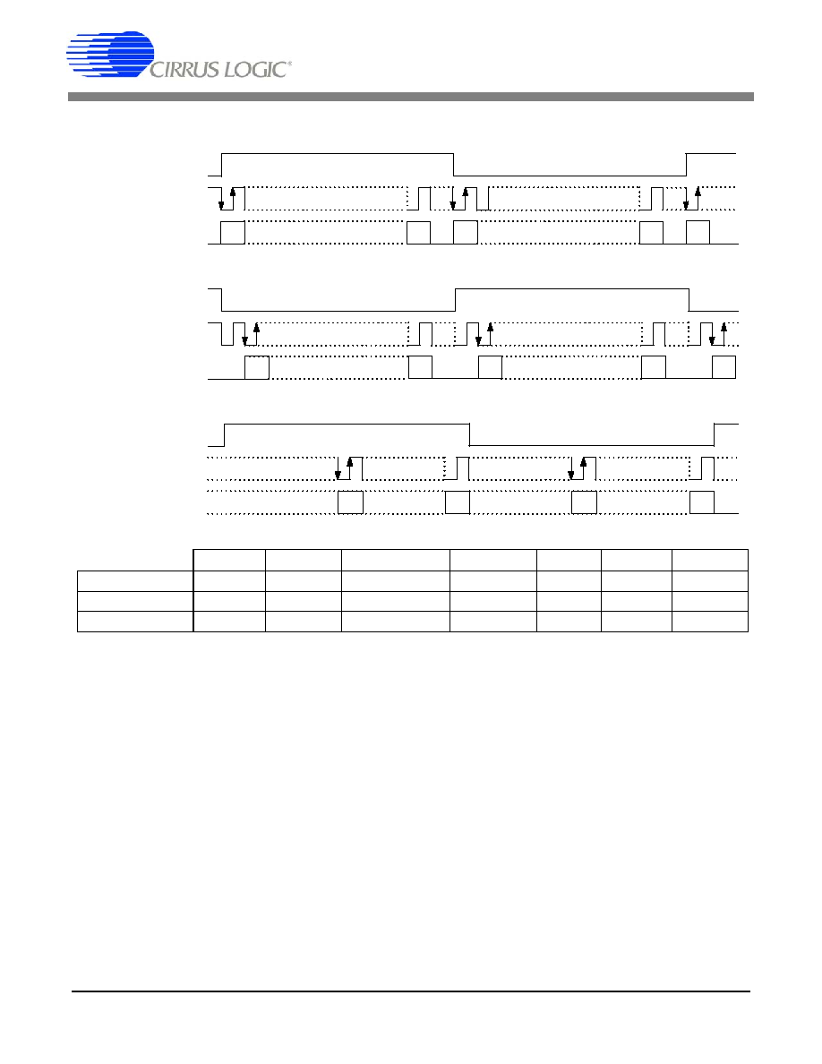
OSCLK Active Edge to SDOUT Output Valid
(Note 8)
t
dpd
-
-
20
ns
SDIN Setup Time Before ISCLK Active Edge
(Note 8)
t
ds
20
-
-
ns
SDIN Hold Time After ISCLK Active Edge
(Note 8)
t
dh
20
-
-
ns
Master Mode
O/RMCK to I/OSCLK active edge delay
(Note 8, 9)
t
smd
0
-
10
ns
O/RMCK to I/OLRCK delay
(Note 10)
t
lmd
0
-
10
ns
I/OSCLK and I/OLRCK Duty Cycle
-
50
-
%
Slave Mode
I/OSCLK Period
(Note 11)
t
sckw
36
-
-
ns
I/OSCLK Input Low Width
t
sckl
14
-
-
ns
I/OSCLK Input High Width
t
sckh
14
-
-
ns
I/OSCLK Active Edge to I/OLRCK Edge
(Note 8, 10, 12)
t
lrckd
20
-
-
ns
I/OLRCK Edge Setup Before I/OSCLK Active Edge
(Note 8, 10, 13)
t
lrcks
20
-
-
ns
sckh
sckl
sckw
t
t
t
tdpd
SDOUT
(input)
(input)
SDIN
dh
t
ds
t
lrcks
t
lrckd
t
ISCLK
OSCLK
ILRCK
OLRCK
t sm d
t lmd
H a rdw a re M o de
S oftw are M o de
IS C L K
O S C L K
(ou tp ut)
ILR C K
O L R C K
(ou tp ut)
R M C K
(ou tp ut)
R M C K
(ou tp ut)
O M C K
(inp ut)
Figure 1. Audio Port Master Mode Timing
Figure 2. Audio Port Slave Mode and Data Input Timing

CS8427
DS477F3
9
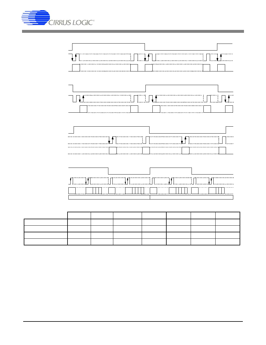
SWITCHING CHARACTERISTICS - CONTROL PORT - SPI MODE
Inputs: Logic 0 = 0 V, Logic 1 = VL+; C
L
= 20 pF.
Notes: 14. If Fso or Fsi is lower than 46.875 kHz, the maximum CCLK frequency should be less than 128 Fso and
less than 128 Fsi. This is dictated by the timing requirements necessary to access the Channel Status
and User Bit buffer memory. Access to the control register file can be carried out at the full 6 MHz rate.
The minimum allowable input sample rate is 8 kHz, so choosing CCLK to be less than or equal to
1.024 MHz should be safe for all possible conditions.
15. Data must be held for sufficient time to bridge the transition time of CCLK.
16. For f
sck
< 1 MHz.
Parameter
Symbol Min Typ
Max
Units
CCLK Clock Frequency
(Note 14)
f
sck
0
-
6.0
MHz
CS High Time Between Transmissions
t
csh
1.0
-
-
µ
s
CS Falling to CCLK Edge
t
css
20
-
-
ns
CCLK Low Time
t
scl
66
-
-
ns
CCLK High Time
t
sch
66
-
-
ns
CDIN to CCLK Rising Setup Time
t
dsu
40
-
-
ns
CCLK Rising to DATA Hold Time
(Note 15)
t
dh
15
-
-
ns
CCLK Falling to CDOUT Stable
t
pd
-
-
50
ns
Rise Time of CDOUT
t
r1
-
-
25
ns
Fall Time of CDOUT
t
f1
-
-
25
ns
Rise Time of CCLK and CDIN
(Note 16)
t
r2
-
-
100
ns
Fall Time of CCLK and CDIN
(Note 16)
t
f2
-
-
100
ns
t r2
t f2
t dsu
t dh
t sch
t scl
CS
CCLK
CDIN
t css
t pd
CDOUT
t csh
Figure 3. SPI Mode timing
CS8427
10
DS477F3
SWITCHING CHARACTERISTICS - CONTROL PORT - I≤C MODE
Note
17
, Inputs: Logic 0 = 0 V, Logic 1 = VL+; C
L
= 20 pF.
Notes: 17. I≤C protocol is supported only in VL+ = 5.0 V mode.
18. Data must be held for sufficient time to bridge the 25 ns transition time of SCL.
Parameter
Symbol Min Typ
Max
Units
SCL Clock Frequency
f
scl
-
-
100
kHz
Bus Free Time Between Transmissions
t
buf
4.7
-
-
µ
s
Start Condition Hold Time (prior to first clock pulse)
t
hdst
4.0
-
-
µ
s
Clock Low Time
t
low
4.7
-
-
µ
s
Clock High Time
t
high
4.0
-
-
µ
s
Setup Time for Repeated Start Condition
t
sust
4.7
-
-
µ
s
SDA Hold Time from SCL Falling
(Note 18)
t
hdd
0
-
-
µ
s
SDA Setup Time to SCL Rising
t
sud
250
-
-
ns
Rise Time of Both SDA and SCL Lines
t
r
-
-
25
ns
Fall Time of Both SDA and SCL Lines
t
f
-
-
25
ns
Setup Time for Stop Condition
t
susp
4.7
-
-
µ
s
t buf
t hdst
t hdst
t
low
t r
t f
t
hdd
t high
t sud
t sust
t susp
Stop
Start
Start
Stop
Repeated
SDA
SCL
Figure 4. I≤C Mode timing

CS8427
DS477F3
11
2. TYPICAL CONNECTION DIAGRAM
* A separate analog supply is only necessary in applications where RMCK is used
for a jitter sensitive task. For applications where RMCK is not used for a jitter
sensitive task, connect VA+ to VD+ via a ferrite bead. Keep the decoupling
capacitor between VA+ and AGND.
CS8427
Cable
Termination
RXP
RXN
AES3/
SPDIF
Source
3-wire Serial
Audio Source
ILRCK
ISCLK
SDIN
Clock Source
and Control
RMCK
OMCK
Hardware
Control
RST
RERR
EMPH
TCBL
To other
CS8427's
Cable
Interface
AES3/
SPDIF
Equipment
TXP
TXN
3-wire Serial
Audio Input
Device
OLRCK
OSCLK
SDOUT
Microcontroller
SDA/CDOUT
AD0/CS
SCL/CCLK
AD1/CDIN
U
INT
VA+
VL+
Ferrite *
Bead
+5.0 V
Analog
Supply*
0.1 F
µ
0.1 F
µ
DGND
FILT
AGND
RFILT
CFILT
CRIP
H/S
+3.3 V or +5.0 V
Digital Supply
D
A 2
/
Figure 5. Recommended Connection Diagram for Software Mode

CS8427
12
DS477F3
3. GENERAL DESCRIPTION
The CS8427 is an AES3 transceiver intended to be
used in digital audio systems. Such systems in-
clude digital mixing consoles, effects processors,
digital recorders, and computer multimedia sys-
tems.
3.1
Audio Input/Output Ports
The CS8427 has the following Audio ports:
∑
Serial Audio Input Port
∑
Serial Audio Output Port
∑
AES3 or S/PDIF Receiver
∑
AES3 or S/PDIF Transmitter
The Serial Audio ports use a three-wire format.
This consists of a serial audio data stream, a left-
right clock defining the boundaries of the audio
sample frames, and a serial clock signal clocking
the data bits.
A Serial Audio port may operate in either Master or
Slave mode. When a port is a Master, it supplies
the left-right clock and the serial clock to the exter-
nal device that is sending or receiving the serial data.
A port in slave mode must have its left-right clock
and its serial clock supplied by an external device
so that it may send or receive serial audio data.
The input sample rate is determined by the stream
applied to the Serial Audio Input or to the AES3 Re-
ceiver. A phase-locked loop recovers RMCK, the
input master clock signal, from the chosen input
stream.
The output from the device may be through the Se-
rial Audio Output, the AES3 Transmitter, or from
both simultaneously. In some configurations, all
audio ports of the device may be in use at the same
time.
3.2
Serial Control Port
Besides the functional blocks already described,
the device also has a control port that allows the
user to read and write the control registers that
configure the part. The control port is capable of
operating in either SPI or I≤C serial mode. This port
also has access to buffer memory that allows the
user to control what is transmitted in the Channel
Status and User bits of the outgoing AES3 stream.
The control port is clocked by the serial clock sig-
nal that the user's microcontroller sends it. The
MCU can read and write the registers even when
the RMCK and OMCK clocks are not running. The
Channel Status and User bit buffer memories de-
pend on clocking from RMCK and OMCK. They will
not function unless the clocks are running, and the
RUN bit in the Clock Source Control register is set.
There is also an interrupt signal associated with
the Serial Control Port and the internal registers.
The format of the interrupt may be chosen by a reg-
ister setting. There are two interrupt status regis-
ters and their associated interrupt mask registers.
3.3
Channel Status and User bit Memory
The memory architecture consists of three buffers
to handle the Channel Status information, and an-
other three buffers to handle the User bits. The
data recovery logic extracts the Channel Status
and User bits from the AES3 stream and places
them in their respective D buffers. Each buffer con-
tains 384 bits.
This is enough memory to hold a complete block of
Channel Status bits from both A and B channels
and a complete block of User bits.
When the D buffers are full, the chip transfers their
contents into the E buffers. While in the E buffers
the Channel Status and User bits may be read or
written through the control port. This allows the
user to alter them to suit the needs of the applica-
tion. The control bit BSEL, in the Channel Status
Data Buffer Control register, determines whether
the control port has access to the Channel Status
bits or the User bits. The AES3 encoder reads the
Channel Status and User bits from the F buffers
and inserts them into the outgoing AES3 stream.
After the F buffers bits are transmitted, the device
transfers the current contents of the E buffers into
the F buffers.
In applications using AES3 in and AES3 out, the
CS8427 can automatically transceive user data
that conforms to the IEC60958 format. The
CS8427 also gives the user access to the bits nec-
essary to comply with the serial copy management
system (SCMS).
In applications where the user want to read/modi-
fy/write the Channel Status information that re-
quires a microcontroller to actively manage the

CS8427
DS477F3
13
Channel Status bits. The part also has a feature
that allows the first five bytes of Channel Status
memory to be configured and transmitted in each
channel status block without change. See
"Appen-
dix A: External AES3/SPDIF/IEC60958 Transmit-
ter and Receiver Components" on page 49
for a
tutorial in Channel Status and User bit manage-
ment.
3.4
AES3 and S/PDIF Standards
Documents
This data sheet assumes that the user is familiar
with the AES3 and S/PDIF data formats. It is advis-
able to have current copies of the AES3 and
IEC60958 specifications on hand for easy refer-
ence.
The latest AES3 standard is available from the Au-
dio Engineering Society or ANSI at
www.aes.org
or
www.ansi.org
. Obtain the latest IEC60958 stan-
dard from ANSI or from the International Electro-
technical Commission at
www.iec.ch
. The latest
EIAJ CP-1201 standard is available from the Jap-
anese Electronics Bureau.
Crystal Application Note AN22: Overview of Digital
Audio Interface Data Structures contains a useful
tutorial on digital audio specifications, but it should
not be considered a substitute for the standards.
The paper, An Understanding and Implementation
of the SCMS Serial Copy Management System for
Digital Audio Transmission, by Clifton Sanchez, is
an excellent tutorial on SCMS. It is available from
the AES as preprint 3518.
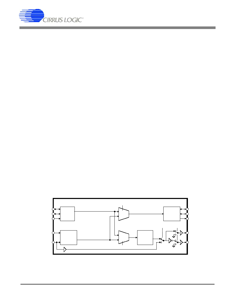
4. DATA I/O FLOW AND CLOCKING
OPTIONS
The CS8427 can be configured for several connec-
tivity alternatives, called data flows.
Figure 7. "Soft-
ware Mode Audio Data Flow Switching Options" on
page 19
shows the data flow switching, along with
the control register bits which control the switches;
this drawing only shows the audio data paths for
simplicity. This drawing only shows the audio data
paths for simplicity.
Figure 8
shows the internal
Serial
Audio
Input
AES3
Encoder
Serial
Audio
Output
Receiver
RXP
RXN
ILRCK
ISCLK
SDIN
OLRCK
OSCLK
SDOUT
TXP
TXN
AES3
TXOFF
AESBP
SPD1-0
TXD1-0
Channel
Status
and
User Data
Recovery
Control
Port
Control
Registers
Channel
Status Bits
D
User Bits
D
E
F
E
F
SDA/CDOUT
SCL/CCLK
AD1/CDIN
AD0/CS
INT
Output
Clock
Generator
OMCK
AD2/EMPH
Figure 6. CS8427 Internal Block Diagram

CS8427
14
DS477F3
clock routing and the associated control register
bits. The clock routing constraints determine which
data routing options are actually usable. Users
should note that not all the possible data flow
switch setting combinations are valid, because of
the clock distribution architecture.
The AESBP switch, shown in
Figure 7
, allows a
TTL level bi-phase, mark-encoded data stream
connected to RXP to be routed to the TXP and
TXN pin drivers. The TXOFF switch causes the
TXP and TXN outputs to be driven to ground.
There are two possible clock sources. The first,
designated the recovered clock, is the output of the
PLL, and is output through the RMCK pin. The in-
put to the PLL can be either the incoming AES3
data stream or the ILRCK word rate clock from the
serial audio input port. The second clock is input
through the OMCK pin and would normally be a
crystal derived stable clock. The Clock Source
Control Register bits determine which clock is used
to operate the CS8427.
The CS8427 has another constraint related to the
state machine that governs the startup of the part.
The startup state machine doesn't complete its
process until the PLL has locked unless one is in
the transmitter dataflow (See
Figure 10
). The con-
sequence of this is that the transmitter will not
transmit until the PLL has locked. If you wish to use
the part in transceiver mode and this constraint is
a problem, there is a work around. Start the part up
in its default configuration and allow the PLL to lock
to a signal on the ILRCK pin, then without stopping
the part, reconfigure it to the transceiver mode.
By studying the following drawings and appropri-
ately setting the Data Flow Control and Clock
Source Control register bits, the CS8427 can be
configured to fit a variety of customer require-
ments. Please note that applications implementing
both the Serial Audio Output Port and the AES3
Transmitter must operate at the same sample rate
because they are both controlled by the same
clock source.
Figure 9
shows the entire data path clocked by the
PLL generated recovered clock.
Figure 10
illus-
trates a standard AES3 receiver function.
Figure
11
shows a standard AES3 transmitter function
without PLL.
Figure 12
shows a standard AES3
transmitter function with PLL.

CS8427
DS477F3
15
5. THREE-WIRE SERIAL AUDIO PORTS
A 3-wire serial audio input port and a 3-wire serial
audio output port is provided. Each port can be ad-
justed to suit the attached device by setting the
control registers. The following parameters are ad-
justable: master or slave, serial clock frequency,
audio data resolution, left or right justification of the
data relative to left/right clock, optional 1-bit cell
delay of the 1st data bit, the polarity of the bit clock,
and the polarity of the left/right clock. By setting the
appropriate control bits, many formats are possi-
ble.
Figure 15
shows a selection of common input for-
mats, along with the control bit settings. It should
be noted that in right justified mode, the serial au-
dio output data is "MSB extended". This means
that in a sub-frame where the MSB of the data is
'1', all bits preceding the MSB in the sub-frame will
also be '1'. Conversely, in a sub-frame where the
MSB of the data is '0', all bits preceding the MSB in
the sub-frame will also be '0'.
The clocking of the input section of the CS8427
may be derived from the incoming ILRCK word
rate clock, using the on-chip PLL. The PLL opera-
tion is described in
"AES3 Receiver" on page 16
. In
the case of use with the serial audio input port, the
PLL locks onto the leading edges of the ILRCK
clock.
Figure 16
shows a selection of common output for-
mats, along with the control bit settings. A special
AES3 direct output format is included, which allows
serial output port access to the V, U, and C bits em-
bedded in the serial audio data stream. The P bit is
replaced by a Z bit that marks the subframe just pri-
or to the start of each block. This format is only
available when the serial audio output port is being
clocked by the AES3 receiver recovered clock.
In master mode, the left/right clock and the serial
bit clock are outputs, derived from the appropriate
clock domain master clock.
In slave mode, the left/right clock and the serial bit
clock are inputs. The left/right clock must be syn-
chronous to the appropriate master clock, but the
serial bit clock can function in asynchronous burst
mode if desired. By appropriate phasing of the
left/right clock and control of the serial clocks,
CS8427's can be multiplexed to share one serial
port. The left/right clock should be continuous, but
the duty cycle does not have to be 50%, provided
that enough serial clocks are present in each
phase to clock all the data bits. When in slave
mode, the serial audio output port must not be set
to right justified data.
When using the serial audio output port in slave
mode with an OLRCK input which is asynchronous
to the port's data source, an interrupt bit (OSLIP) is
provided to indicate when repeated or dropped
samples occur.

CS8427
16
DS477F3
6. AES3 RECEIVER
The CS8427 includes an AES3 digital audio re-
ceiver and an AES3 digital audio transmitter. A
comprehensive buffering scheme provides
read/write access to the channel status and user
data. This buffering scheme is described in "
Ap-
pendix B: Channel Status and User Data Buffer
Management
".
The AES3 receiver accepts and decodes audio
and digital data according to the AES3, IEC60958
(S/PDIF), and EIAJ CP-1201 interface standards.
The receiver consists of a differential input stage,
accessed through pins RXP and RXN, a PLL
based clock recovery circuit, and a decoder which
separates the audio data from the channel status
and user data.
External components are used to terminate and
isolate the incoming data cables from the CS8427.
These components are detailed in
"Appendix A:
External AES3/SPDIF/IEC60958 Transmitter and
Receiver Components" on page 49
.
6.1
OMCK System Clock Mode
A special mode is available that allows the clock
that is being input through the OMCK pin to be out-
put through the RMCK pin. This feature is con-
trolled by the SWCLK bit in control register 1.
When the PLL loses lock, the frequency of the
VCO drops to 300 kHz. The SWCLK function al-
lows the clock from RMCK to be used as a clock in
the system without any disruption when input is re-
moved from the Receiver. This clock switching is
performed glitch free. None of the internal circuitry
that is clocked from the PLL is driven by the OMCK
being output from RMCK. This function is available
only in software mode.
6.2
PLL, Jitter Attenuation, and
Varispeed
Please see Appendix C for general description of
the PLL, selection of recommended PLL filter com-
ponents, and layout considerations. Figure 5
shows the recommended configuration of the two
capacitors and one resistor that comprise the PLL
filter.
6.3
Error Reporting and Hold Function
While decoding the incoming AES3 data stream,
the CS8427 can identify several kinds of error, in-
dicated in the Receiver Error register. The UN-
LOCK bit indicates whether the PLL is locked to
the incoming AES3 data. The V bit reflects the cur-
rent validity bit status. The BIP (bi-phase) error bit
indicates an error in incoming bi-phase coding.
The PAR (parity) bit indicates a received parity er-
ror.
The error bits are "sticky": they are set on the first
occurrence of the associated error and will remain
set until the user reads the register through the
control port. This enables the register to log all un-
masked errors that occurred since the last time the
register was read.
The Receiver Error Mask register allows masking
of individual errors. The bits in this register serve
as masks for the corresponding bits of the Receiv-
er Error Register. If a mask bit is set to 1, the error
is unmasked, which implies the following: its occur-
rence will be reported in the receiver error register,
induce a pulse on RERR, invoke the occurrence of
a RERR interrupt, and affect the current audio
sample according to the status of the HOLD bits.
The HOLD bits allow a choice of holding the previ-
ous sample, replacing the current sample with zero
(mute), or not changing the current audio sample.
If a mask bit is set to 0, the error is masked, which
implies the following: its occurrence will not be re-
ported in the receiver error register, will not induce
a pulse on RERR or generate a RERR interrupt,
and will not affect the current audio sample. The
QCRC and CCRC errors do not affect the current
audio sample, even if unmasked
6.4
Channel Status Data Handling
The first two bytes of the Channel Status block are
decoded into the Receiver Channel Status regis-
ter. The setting of the CHS bit in the Channel Sta-
tus Data Buffer Control register determines
whether the channel status decodes are from the A
channel (CHS = 0) or B channel (CHS = 1).
The PRO (professional) bit is extracted directly.
For consumer data, the COPY (copyright) bit is ex-
tracted, and the category code and L bits are de-
coded to determine SCMS status, indicated by the
ORIG (original) bit. If the category code is set to

CS8427
DS477F3
17
General on the incoming AES3 stream, copyright
will always be indicated even when the stream in-
dicates no copyright. Finally, the AUDIO bit is ex-
tracted and used to set an AUDIO indicator, as
described in the Non-Audio Auto-Detection section
below.
If 50/15 µs pre-emphasis is detected, the state of
the EMPH pin is adjusted accordingly.
The encoded channel status bits which indicate
sample word length are decoded according to
AES3-1992 or IEC 60958. Audio data routed to the
serial audio output port is unaffected by the word
length settings - all 24 bits are passed on as re-
ceived.
"Appendix B: Channel Status and User Data Buffer
Management" on page 51
describes the overall
handling of Channel Status and User bit data.
6.5
User Data Handling
The incoming user data is buffered in a user acces-
sible buffer. Various automatic modes of re-trans-
mitting received User data are provided. The
Appendix: Channel Status and User Data Buffer
Management describes the overall handling of CS
and U data.
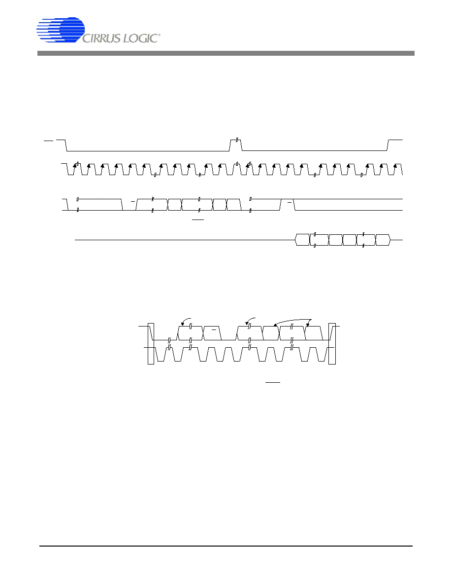
Received User data may also be output to the U
pin, under the control of a control register bit. De-
pending on the data flow and clocking options se-
lected, there may not be a clock available to qualify
the U data output.
Figure 13
illustrates the timing.
If the incoming user data bits have been encoded
as Q-channel subcode, the data is decoded and
presented in ten consecutive register locations. An
interrupt may be enabled to indicate the decoding
of a new Q-channel block, which may be read
through the control port.
6.6
Non-Audio Auto Detection
An AES3 data stream may be used to convey non-
audio data, thus it is important to know whether the
incoming AES3 data stream is digital audio or not.
This information is typically conveyed in channel
status bit 1 (AUDIO), which is extracted automati-
cally by the CS8427. However, certain non-audio
sources, such as AC3
Æ
or MPEG encoders, may
not adhere to this convention, and the bit may not
be properly set. The CS8427 AES3 receiver can
detect such non-audio data. This is accomplished
by looking for a 96-bit sync code, consisting of
0x0000, 0x0000, 0x0000, 0x0000, 0xF872, and
0x4E1F. When the sync code is detected, an inter-
nal AUTODETECT signal will be asserted. If no ad-
ditional sync codes are detected within the next
4096 frames, AUTODETECT will be de-asserted
until another sync code is detected. The AUDIO bit
in the Receiver Channel Status register is the logi-
cal OR of AUTODETECT and the received chan-
nel status bit 1. If non-audio data is detected, the
data is still processed exactly as if it were normal
audio. It is up to the user to mute the outputs as re-
quired.

CS8427
18
DS477F3
7. AES3 TRANSMITTER
The AES3 transmitter encodes and transmits au-
dio and digital data according to the AES3,
IEC60958 (S/PDIF), and EIAJ CP-1201 interface
standards. Audio and control data are multiplexed
together and bi-phase, mark encoded. The result-
ing bit stream is driven to an output connector ei-
ther directly or through a transformer.
The transmitter clock may be derived from the
clock input pin OMCK, or from the incoming data.
If OMCK is asynchronous to the data source, an in-
terrupt bit (TSLIP) is provided that will go high ev-
ery time a data sample is dropped or repeated. Be
aware that the pattern of slips does not have hys-
teresis and so the occurrence of the interrupt con-
dition is not deterministic.
The channel status (C) and user channel (U) bits in
the transmitted data stream are taken from storage
areas within the CS8427. The user can manually
access the internal storage or configure the
CS8427 to run in one of several automatic modes.
The Appendix: Channel Status and User Data
Buffer Management provides detailed descriptions
of each automatic mode and describes methods of
manually accessing the storage areas. The trans-
mitted user data can optionally be input through
the U pin, under the control of a control port regis-
ter bit.
Figure 13
shows the timing requirements for
clocking U data through the U pin.
7.1
Transmitted Frame and Channel
Status Boundary Timing
The TCBL pin is used to control or indicate the start
of transmitted channel status block boundaries and
may be used as an input or output.
In some applications, it may be necessary to con-
trol the precise timing of the transmitted AES3
frame boundaries. This may be achieved in three
ways:
1) With TCBL set to input, driving TCBL high for
>3 OMCK clocks will cause a frame start, as
well as a new channel status block start.
2) If the AES3 output comes from the AES3 input,
setting TCBL as output will cause AES3 output
frame boundaries to align with AES3 input
frame boundaries.
3) If the AES3 output comes from the serial audio
input port while the port is in slave mode and
TCBL is set to output, the start of the A channel
sub-frame will be aligned with the leading edge
of IL-CK.
7.2
TXN and TXP Drivers
The line drivers are low skew, low impedance, dif-
ferential outputs capable of driving cables directly.
Both drivers are set to ground during reset
(RST = low), when no AES3 transmit clock is pro-
vided, and optionally under the control of a register
bit. The CS8427 also allows immediate mute of the
AES3 transmitter audio data through a control reg-
ister bit.
External components are used to terminate and
isolate the external cable from the CS8427. These
components are detailed in
Appendix A: External
AES3/SPDIF/IEC60958 Transmitter and Receiver
Components
.
CS8427
DS477F3
19
8. MONO MODE OPERATION
An AES3 stream may be used in more than one
way to transmit 96-kHz sample rate data. One
method is to double the frame rate of the current
format. This results in a stereo signal with a sample
rate of 96 kHz, carried over a single twisted pair
cable. An alternate method is implemented using
the two sub-frames in a 48-kHz frame rate AES3
signal to carry consecutive samples of a mono sig-
nal, resulting in a 96-kHz sample rate stream. This
allows older equipment, whose AES3 transmitters
and receivers are not rated for 96-kHz frame rate
operation, to handle 96-kHz sample rate informa-
tion. In this "mono mode", two AES3 cables are
needed for stereo data transfer. The CS8427 of-
fers mono mode operation for the AES3 receiver
and the AES3 transmitter. The receiver and trans-
mitter sections may be independently set to mono
mode through the MMR and MMT control bits.
8.1
Receiver Mono Mode
The receiver mono mode effectively doubles the
input frame rate, Fsi. The clock output on the
RMCK pin tracks Fsi, and thus is doubled in fre-
quency compared to stereo mode. The receiver
will run at a frame rate of Fsi/2, and the serial audio
output port will run at Fsi. Sub-frame A data will be
routed to both the left and right data fields on
SD-OUT. Similarly, sub-frame B data will be routed
to both the left and right data fields of the next word
clock cycle of SDOUT.
Using receiver mono mode is only necessary if the
serial audio output port must run at 96 kHz. If the
CS8427 is kept in normal stereo mode and re-
ceives AES3 data arranged in mono mode, the se-
rial audio output port will run at 48 kHz, with left
and right data fields representing consecutive au-
dio samples.
8.2
Transmitter Mono Mode
In transmitter mono mode, the input port will run at
the audio sample rate (Fso), while the AES3 trans-
mitter frame rate will be at Fso/2. Consecutive left
or right channel serial audio data samples may be
selected for transmission on the A and B sub-
frames, and the channel status block transmitted is
also selectable.
Using transmitter mono mode is only necessary if
the incoming audio sample rate is already at
96 kHz and contains both left and right audio data
words. The "mono mode" AES3 output stream may
also be achieved by keeping the CS8427 in normal
stereo mode and placing consecutive audio sam-
ples in the left and right positions of an incoming
data stream with a 48-kHz word rate.
Serial
Audio
Input
AES3
Encoder
Serial
Audio
Output
Receiver
RXP
RXN
ILRCK
ISCLK
SDIN
OLRCK
OSCLK
SDOUT
TXP
TXN
AES3
TXOFF
AESBP
SPD
TXD
MUX
MUX
Figure 7. Software Mode Audio Data Flow Switching Options

CS8427
20
DS477F3
SIMS
PLL
TXP
TXN
SDOUT
OSCLK
OLRCK
OMCK
RMCK
RXP
ILRCK
ISCLK
SDIN
MUX
MUX
MUX
SWCLK
UNLOCK
0
1
0
1
0
1
CHANNEL
STATUS
MEMORY
USER
BIT
MEMORY
TRANSMIT
AES3
SERIAL
AUDIO
OUTPUT
INC
RXD0
MUX
0
1
OUTC
SERIAL
AUDIO
INPUT
RXD1
MUX
0
1
˜
CLK[1:0]
˜
RMCKF
Figure 8. CS8427 Clock Routing
Note: When SWCLK mode is enabled, signal input on OMCK is only output through RMCK and
not routed back through the RXD1 multiplexer; RMCK is not bi-directional in this mode.
*

CS8427
DS477F3
21
AES3
Encoder
& Driver
Serial
Audio
Output
OLRCK
OSCLK
SDOUT
TXP
TXN
PLL
RMCK
TXD1-0:
SPD1-0:
OUTC:
INC:
RXD1-0:
01
10
1
0
01
Clock Source Control Bits
Data Flow Control Bits
AES3
Rx &
Decode
RXP
RXN
Serial
Audio
Input
ILRCK
ISCLK
SDIN
Figure 9. AES3 Input to Serial Audio Output,
Serial Audio Input to AES3 Out
NOTE: Applications implementing both the Seri-
al Audio Output Port and the AES3 Transmitter
must operate at the same sample rate because
they are both controlled by the same clock
source.
OMCK
TXD1-0:
SPD1-0:
OUTC:
INC:
RXD1-0:
01
01
0
1
00
Clock Source Control Bits
Data Flow Control Bits
AES3
Rx &
Decode
I LRCK
I SCLK
SDIN
TXP
TXN
Serial
Audio
Input
Figure 11. Input Serial Port to AES3 Transmitter
without PLL
Serial
Audio
Output
OLRCK
OSCLK
SDOUT
PLL
RMCK
TXD1-0:
SPD1-0:
OUTC:
INC:
RXD1-0:
10
10
1
0
01
Clock Source Control Bits
Data Flow Control Bits
AES3
Rx &
Decode
RXP
RXN
TXOFF : 1
Figure 10. AES3 Input to Serial Audio Output Only
RMCK
TXD1-0:
SPD1-0:
OUTC:
INC:
RXD1-0:
01
01
1
0
00
Clock Source Control Bits
Data Flow Control Bits
AES3
Rx &
Decode
I LRCK
I SCLK
SDIN
TXP
TXN
Serial
Audio
Input
PLL
Figure 12. Input Serial Port to AES3 Transmitter
with PLL
NOTE: In this mode, ILRCK and ISCLK are
inputs only.

CS8427
22
DS477F3
VLRCK
U (Out)
VLRCK is a virtual word clock, which may not exist, but is used to illustrate the U timing.
VLRCK duty cycle is 50%. VLRCK frequency is always equal to the incoming frame rate.
If the serial audio output port is in master mode, VLRCK = OLRCK.
If the serial audio output port is in slave mode, then VLRCK needs to be externally created, if required.
U transitions are aligned within 1% of VLRCK period to VLRCK edges
±
Figure 13. AES3 Receiver Timing for U pin output data
VCU[0]
VCU[1]
VCU[2]
VCU[3]
VCU[4]
VLRCK
Data [4]
Data [5]
Data [6]
Data [7]
Data [8]
Data [0]
Data [1]
Data [2]
Data [3]
Data [4]
TXP(N)
Z
Y
X
Y
X
AES3 Transmitter in Stereo Mode
U[0]
U[2]
TCBL
In or Out
VLRCK
U
Input
Data [4]
Data [5]
Data [6]
Data [7]
Data [8]
SDIN
Input
Data [0]*
Data [2]*
Data [4]*
TXP(N)
Output
Z
Y
X
* Assume MMTLR = 0
Tsetup => 7.5% AES3 frame time
Thold = 0
Tsetup
Thold
Data [1]*
Data [3]*
Data [5]*
TXP(N)
Output
Z
Y
X
AES3 Transmitter in Mono Mode
* Assume MMTLR = 1
Tsetup => 15% AES3 frame time
Thold = 0
VLRCK is a virtual word clock, which may not exist, is used to illustrate the CUV timing.
VLRCK duty cycle is 50%.
In stereo mode, VLRCK frequency = AES3 frame rate. In mono mode, ALRCK frequency = 2xAES3 frame rate.
If the serial audio input port is on slave mode and TCBL is an output, then VLRCK=ILRCK if SILRPOL=0 and
VLRCK= ILRCK if SILRPOL =1.
If the serial audio input port is in master mode and TCBL is an input, then VLRCK=ILRCK if SILRPOL=0 and
VLRCK= ILRCK if SILRPOL =1.
Tth
Tth > 3OMCK if TCBL is Input
Tth > 3OMCK if TCBL is Input
Tth
Figure 14. AES3 Transmitter Timing for C, U and V pin input data
CS8427
DS477F3
23
MSB
LSB
MSB
LSB
MSB
ILRCK
ISCLK
SDIN
Channel A
Channel B
Left
Justified
(In)
ILRCK
ISCLK
MSB
LSB
MSB
LSB
Channel A
SDIN
MSB
Channel B
I≤S
(In)
ILRCK
ISCLK
Channel A
Channel B
MSB
SDIN
MSB
LSB
LSB
Right
Justified
(In)
Figure 15. Serial Audio Input Example Formats
X = don't care to match format, but does need to be set to the desired setting
+ I≤S can accept an arbitrary number of bits, determined by the number of ISCLK cycles
* See Serial Input Port Data Format Register Bit Descriptions for an explanation of the meaning of each bit
SIMS*
SISF*
SIRES*[1:0]
SIJUST*
SIDEL*
SISPOL* SILRPOL*
Left Justified
X
X
00+
0
0
0
0
I≤S
X
X
00+
0
1
0
1
Right Justified
X
X
XX
1
0
0
0
CS8427
24
DS477F3
OLRCK
OSCLK
SDOUT
Channel A
Channel B
Left
Justified
(Out)
OLRCK
OSCLK
Channel A
SDOUT
Channel B
I≤S
(Out)
OLRCK
OSCLK
Channel A
Channel B
MSB
SDOUT
MSB
LSB
LSB
MSB Extended
MSB Extended
Right
Justified
(Out)
OLRCK
OSCLK
Channel A
Channel B
MSB
SDOUT
LSB
LSB
Channel A
Channel B
LSB
LSB
MSB
MSB
MSB
AES3
Direct
(Out)
MSB
MSB
MSB
LSB
LSB
MSB
LSB
MSB
LSB
MSB
C
U
V
Z
C
U
V
Z
C
U
V
C
U
V
Frame 191
Frame 0
Figure 16. Serial Audio Output Example Formats
X = don't care to match format, but does need to be set to the desired setting
* See Serial Output Data Format Register Bit Descriptions for an explanation of the meaning of each bit
SOMS*
SOSF*
SORES[1:0]* SOJUST*
SODEL*
SOSPOL* SOLRPOL*
Left Justified
X
X
XX
0
0
0
0
I≤S
X
X
XX
0
1
0
1
Right Justified
1
X
XX
1
0
0
0
AES3 Direct
X
X
11
0
0
0
0

CS8427
DS477F3
25
9. CONTROL PORT DESCRIPTION AND
TIMING
The control port is used to access the registers, al-
lowing the CS8427 to be configured for the desired
operational modes and formats. In addition, Chan-
nel Status and User data may be read and written
through the control port. The operation of the con-
trol port may be completely asynchronous with re-
spect to the audio sample rates. However, to avoid
potential interference problems, the control port
pins should remain static if no operation is re-
quired.
The control port has two modes: SPI and I≤C, with
the CS8427 acting as a slave device. SPI mode is
selected if there is a high to low transition on the
AD0/CS pin after the RST pin has been brought
high. I≤C mode is selected by connecting the
AD0/CS pin to VL+ or DGND, thereby permanently
selecting the desired AD0 bit address state.
9.1
SPI
TM
Mode
In SPI mode, CS is the CS8427 chip select signal;
CCLK is the control port bit clock (input into the
CS8427 from the microcontroller); CDIN is the in-
put data line from the microcontroller; CDOUT is
the output data line to the microcontroller. Data is
clocked in on the rising edge of CCLK and out on
the falling edge.
Figure 17
shows the operation of the control port in
SPI mode. To write to a register, bring CS low. The
first seven bits on CDIN form the chip address and
must be 0010000b. The eighth bit is a read/write
indicator (R/W), which should be low to write. The
next eight bits form the Memory Address Pointer
(MAP), which is set to the address of the register
that is to be updated. The next eight bits are the
data which will be placed into the register designat-
ed by the MAP. During writes, the CDOUT output
stays in the Hi-Z state. It may be externally pulled
high or low with a 47 k
resistor, if desired.
There is a MAP auto increment capability, enabled
by the INCR bit in the MAP register. If INCR is a ze-
ro, the MAP will stay constant for successive read
or writes. If INCR is set to a 1, then the MAP will au-
toincrement after each byte is read or written, al-
lowing block reads or writes of successive
registers.
To read a register, the MAP has to be set to the
correct address by executing a partial write cycle
which finishes (CS high) immediately after the
MAP byte. The MAP auto increment bit (INCR)
may be set or not, as desired. To begin a read,
bring CS low, send out the chip address, and set
the read/write bit (R/W) high. The next falling edge
of CCLK will clock out the MSB of the addressed
register (CDOUT will leave the high impedance
state). If the MAP auto increment bit is set to 1, the
data for successive registers will appear consecu-
tively.
9.2
I≤C Mode
In I≤C mode, SDA is a bidirectional data line. Data
is clocked into and out of the part by SCL, with the
clock to data relationship as shown in
Figure 18
.
There is no CS pin. Each individual CS8427 is giv-
en a unique address. Pins AD0 and AD1 form the
two least significant bits of the chip address and
should be connected to VL+ or DGND as desired.
The EMPH pin is used to set the AD2 bit, by con-
necting a resistor from the EMPH pin to VL+ or to
DGND. The state of the pin is sensed while the
CS8427 is being reset. The upper four bits of the
seven bit address field are fixed at 0010b. To com-
municate with a CS8427, the chip address field,
which is the first byte sent to the CS8427, should
be 0010b followed by the settings of the EMPH,
AD1, and AD0. The eighth bit of the address is the
R/W bit. If the operation is a write, the next byte is
the Memory Address Pointer (MAP) which selects
the register to be read or written. If the operation is
a read, the contents of the register pointed to by
the MAP will be output. Setting the auto increment
bit in MAP allows successive reads or writes of
consecutive registers. Each byte is separated by
an acknowledge bit, ACK, which is output from the
CS8427 after each input byte is read. The ACK bit
is input to the CS8427 from the microcontroller af-
ter each transmitted byte. I≤C mode is supported
only with VL+ = 5.0 V.
9.3
Interrupts
The CS8427 has a comprehensive interrupt capa-
bility. The INT output pin is intended to drive the in-
terrupt input pin on the host microcontroller. The
INT pin may be set to be active low, active high, or
active low with no active pull-up transistor. This last
CS8427
26
DS477F3
mode is used for active-low, wired-OR hook-ups
with multiple peripherals connected to the micro-
controller interrupt input pin.
Many conditions can cause an interrupt, as listed in
the interrupt status register descriptions. Each
source may be masked off using mask register
bits. In addition, each source may be set to rising
edge, falling edge, or level-sensitive. Combined
with the option of level-sensitive or edge-sensitive
modes within the microcontroller, many different
set-ups are possible depending on the needs of
the equipment designer.
M A P
MSB
LSB
DATA
b y te 1
b y te n
R/W
R/W
A D D R E S S
C H IP
ADDRESS
C H IP
C D IN
C C L K
CS
C D O U T
MSB
LSB MSB
LSB
0010000
0010000
MAP = Memory Address Pointer, 8 bits, MSB first
High Impedance
Figure 17. Control Port Timing in SPI Mode
SDA
SCL
0010
AD2-0
R/W
Start
ACK DATA7-0 ACK DATA7-0 ACK
Stop
Note 2
Note 1
Note 1: AD2 is derived from a resistor attached to the EMPH pin,
Note 2: If operation is a write, this byte contains the Memory Address Pointer, MAP
AD1 and AD0 are determined by the state of the corresponding pins
Note 3: If operation is a read, the last bit of the read should be a NACK(high)
Note 3
Figure 18. Control Port Timing in I≤C Mode

CS8427
DS477F3
27
10. CONTROL PORT REGISTER SUMMARY
10.1 Memory Address Pointer (MAP)
INCR - Auto Increment Address Control Bit
Default = `0'
0 - Disable
1 - Enable
MAP6:MAP0 - Register address
Note: Reserved registers must not be written to during normal operation. Some reserved registers are used for test
modes, which can completely alter the normal operation of the CS8427.
Addr
(HEX)
Function
7
6
5
4
3
2
1
0
00
Reserved
0
0
0
0
0
0
0
0
01
Control 1
SWCLK
VSET
MUTESAO
MUTEAES
0
INT1
INT0
TCBLD
02
Control 2
0
HOLD1
HOLD0
RMCKF
MMR
MMT
MMTCS
MMTLR
03
Data Flow Control
0
TXOFF
AESBP
TXD1
TXD0
SPD1
SPD0
0
04
Clock Source Control
0
RUN
CLK1
CLK0
OUTC
INC
RXD1
RXD0
05
Serial Input Format
SIMS
SISF
SIRES1
SIRES0
SIJUST
SIDEL
SISPOL
SILRPOL
06
Serial Output Format
SOMS
SOSF
SORES1
SORES0
SOJUST
SODEL
SOSPOL
SOLRPOL
07
Interrupt 1 Status
TSLIP
OSLIP
0
0
0
DETC
EFTC
RERR
08
Interrupt 2 Status
0
0
0
0
EFTU
QCH
0
09
Interrupt 1 Mask
TSLIPM
OSLIPM
0
0
0
DETCM
EFTCM
RERRM
0A
Interrupt 1 Mode (MSB)
TSLIP1
OSLIP1
0
0
0
DETC1
EFTC1
RERR1
0B
Interrupt 1 Mode (LSB)
TSLIP0
OSLIP0
0
0
0
DETC0
EFTC0
RERR0
0C
Interrupt 2 Mask
0
0
0
0
DETUM
EFTUM
QCHM
0
0D
Interrupt 2 Mode (MSB)
0
0
0
0
DETU1
EFTU1
QCH1
0
0E
Interrupt 2 Mode (LSB)
0
0
0
0
DETU0
EFTU0
QCH0
0
0F
Receiver CS Data
AUX3
AUX2
AUX1
AUX0
PRO
AUDIO
COPY
ORIG
10
Receiver Errors
0
QCRC
CCRC
UNLOCK
V
CONF
BIP
PAR
11
Receiver Error Mask
0
QCRCM
CCRCM
UNLOCKM
VM
CONFM
BIPM
PARM
12
CS Data Buffer Control
0
0
BSEL
CBMR
DETCI
EFTCI
CAM
CHS
13
U Data Buffer Control
0
0
0
UD
UBM1
UBM0
DETUI
EFTUI
14-1D Q sub-code Data
1E
OMCK/RMCK Ratio
ORR7
ORR6
ORR5
ORR4
ORR3
ORR2
ORR1
ORR0
1F
Reserved
20-37 C or U Data Buffer
7F
ID and Version
ID3
ID2
ID1
ID0
VER3
VER2
VER1
VER0
Table 1. Control Register Map Summary
7
6
5
4
3
2
1
0
INCR
MAP6
MAP5
MAP4
MAP3
MAP2
MAP1
MAP0
CS8427
28
DS477F3
11. CONTROL PORT REGISTER BIT DEFINITIONS
11.1 Control 1 (01h)
SWCLK - Controls output of OMCK on RMCK when PLL loses lock
Default = `0'
0 - RMCK default function
1 - OMCK output on RMCK pin
VSET - Transmitted Validity bit level
Default = `0'
0 - Indicates data is valid, linear PCM audio data
1 - Indicates data is invalid or not linear PCM audio data
MUTESAO - Mute control for the serial audio output port
Default = `0'
0 - Not Muted
1 - Muted
MUTEAES - Mute control for the AES transmitter output
Default = `0'
0 - Not Muted
1 - Muted
INT1:INT0 - Interrupt output pin (INT) control
Default = `00'
00 - Active high; high output indicates interrupt condition has occurred
01 - Active low, low output indicates an interrupt condition has occurred
10 - Open drain, active low. Requires an external pull up resistor on the INT pin.
11 - Reserved
TCBLD - Transmit Channel Status Block pin (TCBL) direction specifier
Default = `0'
0 - TCBL is an input
1 - TCBL is an output
11.2 Control 2 (02h)
HOLD1:HOLD0 - Determine how received audio sample is affected when a receiver error occurs
Default = `00'
00 - Hold the last valid audio sample
01 - Replace the current audio sample with 00 (mute)
10 - Do not change the received audio sample
11 - Reserved
RMCKF - Select recovered master clock output pin frequency.
Default = `0'
0 - RMCK is equal to 256 * Fsi
1 - RMCK is equal to 128 * Fsi
7
6
5
4
3
2
1
0
SWCLK
VSET
MUTESAO
MUTEAES
0
INT1
INT0
TCBLD
7
6
5
4
3
2
1
0
0
HOLD1
HOLD0
RMCKF
MMR
MMT
MMTCS
MMTLR

CS8427
DS477F3
29
MMR - Select AES3 receiver mono or stereo operation
Default = `0'
0 - Normal stereo operation
1 - A and B subframes treated as consecutive samples of one channel of data. Data is duplicated to
both left and right parallel outputs of the AES receiver block. The input sample rate (Fsi) is doubled
compared to MMR=0
MMT - Select AES3 transmitter mono or stereo operation
Default = `0'
0 - Normal stereo operation
1 - Output either left or right channel inputs into consecutive subframe outputs (mono
mode, left or right is determined by MMTLR bit)
MMTCS - Select A or B channel status data to transmit in mono mode
Default = `0'
0 - Use channel A CS data for the A subframe and use channel B CS data for the B subframe
1 - Use the same CS data for both the A and B subframe outputs. If MMTLR = 0, use the
left channel CS data. If MMTLR = 1, use the right channel CS data.
MMTLR - Channel Selection for AES Transmitter mono mode
Default = `0'
0 - Use left channel input data for consecutive subframe outputs
1- Use right channel input data for consecutive subframe outputs
11.3 Data Flow Control (03h)
The Data Flow Control register configures the flow of audio data to/from the following blocks: Serial Audio Input Port,
Serial Audio Output Port, AES3 receiver, and AES3 transmitter. In conjunction with the Clock Source Control regis-
ter, multiple Receiver/Transmitter/Transceiver modes may be selected. The output data should be muted prior to
changing bits in this register to avoid transients.
TXOFF - AES3 Transmitter Output Driver Control
Default = `0
0 - AES3 transmitter output pin drivers normal operation
1 - AES3 transmitter output pin drivers drive to 0 V.
AESBP - AES3 bypass mode selection
Default = `0'
0 - Normal operation
1 - Connect the AES3 transmitter driver input directly to the RXP pin, which becomes a normal TTL
threshold digital input. The transmitter clock (selecting using the OUTC bit in the Clock Source Control)
must be present for the bypass mode to work.
TXD1:TXD0 - AES3 Transmitter Data Source
Default = `01'
00 - Reserved
01 - Serial audio input port
10 - AES3 receiver
11 - Reserved
7
6
5
4
3
2
1
0
0
TXOFF
AESBP
TXD1
TXD0
SPD1
SPD0
0

CS8427
30
DS477F3
SPD1:SPD0 - Serial Audio Output Port Data Source
Default = `10'
00 - Reserved
01 - Serial Audio Input Port
10 - AES3 receiver
11 - Reserved
11.4 Clock Source Control (04h)
This register configures the clock sources of various blocks. In conjunction with the Data Flow Control register, var-
ious Receiver/Transmitter/Transceiver modes may be selected.
RUN - Controls the internal clocks, allowing the CS8427 to be placed in a "powered down", low current consumption,
state.
Default = `0'
0 - Internal clocks are stopped. Internal state machines are reset. The fully static
control port is operational, allowing registers to be read or changed. Reading and
writing the U and C data buffers is not possible. Power consumption is low.
1 - Normal part operation. This bit must be written to the 1 state to allow the CS8427
to begin operation. All input clocks should be stable in frequency and phase when
RUN is set to 1.
CLK1:0 - Output side master clock input (OMCK) frequency to output sample rate (Fso) ratio selector. If these bits
are changed during normal operation, then always stop the CS8427 first (RUN = 0), write the new value, then start
the CS8427 (RUN = 1).
Default = `00'
00 - OMCK frequency is 256 * Fso
01 - OMCK frequency is 384 * Fso
10 - OMCK frequency is 512 * Fso
11 - Reserved
OUTC - Output Time Base
Default = `0'
0 - OMCK input pin, modified by the selected divide ratio bits CLK1:0.
1 - Recovered Input Clock
INC - Input Time Base Clock Source
Default = `0'
0 - Recovered Input Clock
1 - OMCK input pin, modified by the selected divide ratio bits CLK1:0.
RXD1:0 - Recovered Input Clock Source
Default = `00'
00 - 256 * Fsi, where Fsi is derived from the ILRCK pin (only possible when the
serial audio input port is in slave mode)
01 - 256 * Fsi, where Fsi is derived from the AES3 input frame rate
10 - Bypass the PLL and apply an external 256 * Fsi clock through the RMCK pin. The AES3
receiver is held in synchronous reset. This setting is useful to prevent UNLOCK
interrupts when using an external RMCK and inputting data through the serial audio input port.
11 - Reserved.
7
6
5
4
3
2
1
0
0
RUN
CLK1
CLK0
OUTC
INC
RXD1
RXD0

CS8427
DS477F3
31
11.5 Serial Audio Input Port Data Format (05h)
SIMS - Master/Slave Mode Selector
Default = `0'
0 - Serial audio input port is in slave mode
1 - Serial audio input port is in master mode
SISF - ISCLK frequency (for master mode)
Default = `0'
0 - 64 * Fsi
1 - 128 * Fsi
SIRES1:0 - Resolution of the input data, for right-justified formats
Default = `00'
00 - 24 bit resolution
01 - 20 bit resolution
10 - 16 bit resolution
11 - Reserved
SIJUST - Justification of SDIN data relative to ILRCK
Default = `0'
0 - Left-justified
1 - Right-justified
SIDEL - Delay of SDIN data relative to ILRCK, for left-justified data formats
Default = `0'
0 - MSB of SDIN data occurs in the first ISCLK period after the ILRCK edge
1 - MSB of SDIN data occurs in the second ISCLK period after the ILRCK edge
SISPOL - ISCLK clock polarity
Default = `0'
0 - SDIN sampled on rising edges of ISCLK
1 - SDIN sampled on falling edges of ISCLK
SILRPOL - ILRCK clock polarity
Default = `0'
0 - SDIN data is for the left channel when ILRCK is high
1 - SDIN data is for the right channel when ILRCK is high
11.6 Serial Audio Output Port Data Format (06h)
SOMS - Master/Slave Mode Selector
Default = `0'
0 - Serial audio output port is in slave mode
1 - Serial audio output port is in master mode
SOSF - OSCLK frequency (for master mode)
Default = `0'
0 - 64 * Fso
1 - 128 * Fso
7
6
5
4
3
2
1
0
SIMS
SISF
SIRES1
SIRES0
SIJUST
SIDEL
SISPOL
SILRPOL
7
6
5
4
3
2
1
0
SOMS
SOSF
SORES1
SORES0
SOJUST
SODEL
SOSPOL
SOLRPOL

CS8427
32
DS477F3
SORES1:0 - Resolution of the output data on SDOUT and on the AES3 output
Default = `00'
00 - 24-bit resolution
01 - 20-bit resolution
10 - 16-bit resolution
11 - Direct copy of the received NRZ data from the AES3 receiver (including C, U, and
V bits, the time slot normally occupied by the P bit is used to indicate the location
of the block start, SDOUT pin only, serial audio output port clock must be derived
from the AES3 receiver recovered clock)
SOJUST - Justification of SDOUT data relative to OLRCK
Default = `0'
0 - Left-justified
1 - Right-justified (master mode only)
SODEL - Delay of SDOUT data relative to OLRCK, for left-justified data formats
Default = `0'
0 - MSB of SDOUT data occurs in the first OSCLK period after the OLRCK edge
1 - MSB of SDOUT data occurs in the second OSCLK period after the OLRCK edge
SOSPOL - OSCLK clock polarity
Default = `0'
0 - SDOUT transitions occur on falling edges of OSCLK
1 - SDOUT transitions occur on rising edges of OSCLK
SOLRPOL - OLRCK clock polarity
Default = `0'
0 - SDOUT data is for the left channel when OLRCK is high
1 - SDOUT data is for the right channel when OLRCK is high
11.7 Interrupt 1 Status (07h) (Read Only)
For all bits in this register, a "1" means the associated interrupt condition has occurred at least once since the register
was last read. A "0" means the associated interrupt condition has NOT occurred since the last reading of the register.
Reading the register resets all bits to 0, unless the interrupt mode is set to level and the interrupt source is still true.
Status bits that are masked off in the associated mask register will always be "0" in this register. This register defaults
to 00h.
TSLIP - AES3 transmitter source data slip interrupt.
In data flows where OMCK, which clocks the AES3 transmitter, is asynchronous to the data source, this
bit will go high every time a data sample is dropped or repeated. When TCBL is an input, this bit will go
high on receipt of a new TCBL signal.
OSLIP - Serial audio output port data slip interrupt.
When the serial audio output port is in slave mode, and OLRCK is asynchronous to the port data source,
this bit will go high every time a data sample is dropped or repeated.
DETC - D to E C-buffer transfer interrupt.
Indicates the completion of a D to E C-buffer transfer. See "Channel Status and User Data Buffer Man-
agement" on page 51 for more information.
EFTC - E to F C-buffer transfer interrupt.
Indicates the completion of a E to F C-buffer transfer. See "Channel Status and User Data Buffer Man-
agement" on page 51 for more information.
RERR - A receiver error has occurred.
The Receiver Error register may be read to determine the nature of the error which caused the interrupt.
7
6
5
4
3
2
1
0
TSLIP
OSLIP
0
0
0
DETC
EFTC
RERR

CS8427
DS477F3
33
11.8 Interrupt 2 Status (08h) (Read Only)
For all bits in this register, a "1" means the associated interrupt condition has occurred at least once since the register
was last read. A "0" means the associated interrupt condition has NOT occurred since the last reading of the register.
Reading the register resets all bits to 0, unless the interrupt mode is set to level and the interrupt source is still true.
Status bits that are masked off in the associated mask register will always be "0" in this register. This register defaults
to 00h.
DETU - D to E U-buffer transfer interrupt. (Block Mode only)
Indicates the completion of a D to E U-buffer transfer. See "Channel Status and User Data Buffer Man-
agement" on page 51 for more information.
EFTU - E to F U-buffer transfer interrupt. (Block Mode only)
Indicates the completion of a E to F U-buffer transfer. See "Channel Status and User Data Buffer Man-
agement" on page 51 for more information.
QCH - A new block of Q-subcode data is available for reading.
The data must be completely read within 588 AES3 frames after the interrupt occurs to avoid corruption
of the data by the next block.
11.9 Interrupt 1 Mask (09h)
The bits of this register serve as a mask for the Interrupt 1 register. If a mask bit is set to 1, the error is unmasked,
meaning that its occurrence will affect the INT pin and the status register. If a mask bit is set to 0, the error is masked,
meaning that its occurrence will not affect the INT pin or the status register. The bit positions align with the corre-
sponding bits in the Interrupt 1 register. This register defaults to 00h.
11.10 Interrupt 1 Mode MSB (0Ah) & Interrupt 1 Mode LSB (0Bh)
The two Interrupt Mode registers form a 2-bit code for each Interrupt Register 1 function. There are three ways to
set the INT pin active in accordance with the interrupt condition. In the Rising edge active mode, the INT pin be-
comes active on the arrival of the interrupt condition. In the Falling edge active mode, the INT pin becomes active
on the removal of the interrupt condition. In Level active mode, the INT interrupt pin becomes active during the in-
terrupt condition. Be aware that the active level (Active High or Low) only depends on the INT[1:0] bits. These reg-
isters default to 00.
00 - Rising edge active
01 - Falling edge active
10 - Level active
11 - Reserved
7
6
5
4
3
2
1
0
0
0
0
0
DETU
EFTU
QCH
0
7
6
5
4
3
2
1
0
TSLIPM
OSLIPM
0
0
0
DETCM
EFTCM
RERRM
7
6
5
4
3
2
1
0
TSLIP1
OSLIP1
0
0
0
DETC1
EFTC1
RERR1
TSLIP0
OSLIP0
0
0
0
DETC0
EFTC0
RERR0

CS8427
34
DS477F3
11.11 Interrupt 2 Mask (0Ch)
The bits of this register serve as a mask for the Interrupt 2 register. If a mask bit is set to 1, the error is unmasked,
meaning that its occurrence will affect the INT pin and the status register. If a mask bit is set to 0, the error is masked,
meaning that its occurrence will not affect the INT pin or the status register. The bit positions align with the corre-
sponding bits in the Interrupt 2 register. This register defaults to 00h.
11.12 Interrupt 2 Mode MSB (0Dh) & Interrupt 2 Mode LSB (0Eh)
The two Interrupt Mode registers form a 2-bit code for each Interrupt Register 1 function. There are three ways to
set the INT pin active in accordance with the interrupt condition. In the Rising edge active mode, the INT pin be-
comes active on the arrival of the interrupt condition. In the Falling edge active mode, the INT pin becomes active
on the removal of the interrupt condition. In Level active mode, the INT interrupt pin becomes active during the in-
terrupt condition. Be aware that the active level (Active High or Low) only depends on the INT[1:0] bits. These reg-
isters default to 00.
00 - Rising edge active
01 - Falling edge active
10 - Level active
11 - Reserved
11.13 Receiver Channel Status (0Fh) (Read Only)
The bits in this register can be associated with either channel A or B of the received data. The desired channel is
selected with the CHS bit of the Channel Status Data Buffer Control Register.
AUX3:0 - Incoming auxiliary data field width, as indicated by the incoming channel status bits, decoded according
to IEC60958 and AES3.
0000 - Auxiliary data is not present
0001 - Auxiliary data is 1 bit long
0010 - Auxiliary data is 2 bits long
0011 - Auxiliary data is 3 bits long
0100 - Auxiliary data is 4 bits long
0101 - Auxiliary data is 5 bits long
0110 - Auxiliary data is 6 bits long
0111 - Auxiliary data is 7 bits long
1000 - Auxiliary data is 8 bits long
1001 - 1111 Reserved
PRO - Channel status block format indicator
0 - Received channel status block is in consumer format
1 - Received channel status block is in professional format
7
6
5
4
3
2
1
0
0
0
0
0
DETUM
EFTUM
QCHM
0
7
6
5
4
3
2
1
0
0
0
0
0
DETU1
EFTU1
QCH1
0
0
0
0
0
DETU0
EFTU0
QCH0
0
7
6
5
4
3
2
1
0
AUX3
AUX2
AUX1
AUX0
PRO
AUDIO
COPY
ORIG

CS8427
DS477F3
35
AUDIO - Audio indicator
0 - Received data is linearly coded PCM audio
1 - Received data is not linearly coded PCM audio
COPY - SCMS copyright indicator
0 - Copyright asserted
1 - Copyright not asserted
If the category code is set to General in the incoming AES3 stream, copyright will always be indicated by COPY,
even when the stream indicates no copyright.
ORIG - SCMS generation indicator, decoded from the category code and the L bit.
0 - Received data is 1st generation or higher
1 - Received data is original
Note: COPY and ORIG will both be set to 1 if the incoming data is flagged as professional, or if the receiver is not
in use.
11.14 Receiver Error (10h) (Read Only)
This register contains the AES3 receiver and PLL status bits. Unmasked bits will go high on occurrence of the error,
and will stay high until the register is read. Reading the register resets all bits to 0, unless the error source is still
true. Bits that are masked off in the receiver error mask register will always be 0 in this register.
QCRC - Q-subcode data CRC error indicator. Updated on Q-subcode block boundaries
0 - No error
1 - Error
CCRC - Channel Status Block Cyclic Redundancy Check bit. Updated on CS block boundaries, valid in Pro mode.
0 - No error
1 - Error
UNLOCK - PLL lock status bit. Updated on CS block boundaries.
0 - PLL locked
1 - PLL out of lock
V - Received AES3 Validity bit status. Updated on sub-frame boundaries.
0 - Data is valid and is normally linear coded PCM audio
1 - Data is invalid, or may be valid compressed audio
CONF - Confidence bit. Updated on sub-frame boundaries.
0 - No error
1 - Confidence error. This is the logical OR of BIP and UNLOCK.
BIP - Bi-phase error bit. Updated on sub-frame boundaries.
0 - No error
1 - Bi-phase error. This indicates an error in the received bi-phase coding.
PAR - Parity bit. Updated on sub-frame boundaries.
0 - No error
1 - Parity error
7
6
5
4
3
2
1
0
0
QCRC
CCRC
UNLOCK
V
CONF
BIP
PAR

CS8427
36
DS477F3
11.15 Receiver Error Mask (11h)
The bits in this register serve as masks for the corresponding bits of the Receiver Error register. If a mask bit is set
to 1, the error is unmasked, meaning that its occurrence will appear in the receiver error register, will affect the RERR
pin, will affect the RERR interrupt, and will affect the current audio sample according to the status of the HOLD bit.
If a mask bit is set to 0, the error is masked, meaning that its occurrence will not appear in the receiver error register,
will not affect the RERR pin, will not affect the RERR interrupt, and will not affect the current audio sample. The
CCRC and QCRC bits behave differently from the other bits: they do not affect the current audio sample even when
unmasked. This register defaults to 00h.
11.16 Channel Status Data Buffer Control (12h)
BSEL - Selects the data buffer register addresses to contain User data or Channel Status data
Default = `0'
0 - Data buffer address space contains Channel Status data
1 - Data buffer address space contains User data
CBMR - Control for the first 5 bytes of channel status "E" buffer
Default = `0'
0 - Allow D to E buffer transfers to overwrite the first 5 bytes of channel status data
1 - Prevent D to E buffer transfers from overwriting first 5 bytes of channel status data
DETCI - D to E C-data buffer transfer inhibit bit.
Default = `0'
0 - Allow C-data D to E buffer transfers
1 - Inhibit C-data D to E buffer transfers
EFTCI - E to F C-data buffer transfer inhibit bit.
Default = `0'
0 - Allow C-data E to F buffer transfers
1 - Inhibit C-data E to F buffer transfers
CAM - C-data buffer control port access mode bit
Default = `0'
0 - One byte mode
1 - Two byte mode
CHS - Channel select bit
Default = `0'
0 - Channel A information is displayed at the EMPH pin and in the receiver channel
status register. Channel A information is output during control port reads when
CAM is set to 0 (One Byte Mode)
1 - Channel B information is displayed at EMPH pin and in the receiver channel
status register. Channel B information is output during control port reads when
CAM is set to 0 (One Byte Mode)
7
6
5
4
3
2
1
0
0
QCRCM
CCRCM
UNLOCKM
VM
CONFM
BIPM
PARM
7
6
5
4
3
2
1
0
0
0
BSEL
CBMR
DETCI
EFTCI
CAM
CHS
CS8427
DS477F3
37
11.17 User Data Buffer Control (13h)
UD - User data pin (U) direction specifier If this bit is changed during normal operation, then always stop the CS8427
first (RUN = 0), write the new value, then start the CS8427 (RUN = 1).
Default = `0'
0 - The U pin is an input. The U data is latched in on both rising and falling edges of
OLRCK. This setting also chooses the U pin as the source for transmitted U data.
1 - The U pin is an output. The received U data is clocked out on both rising and falling edges
of ILRCK. This setting also chooses the U data buffer as the source of transmitted U data.
UBM1:0 - Sets the operating mode of the AES3 U bit manager
Default = `00'
00 - Transmit all zeros mode
01 - Block mode
10 - Reserved
11 - Reserved
DETUI - D to E U-data buffer transfer inhibit bit (valid in block mode only).
Default = `0'
0 - Allow U-data D to E buffer transfers
1 - Inhibit U-data D to E buffer transfers
EFTUI - E to F U-data buffer transfer inhibit bit (valid in block mode only).
Default = `0'
0 - Allow U-data E to F buffer transfers
1 - Inhibit U-data E to F buffer transfer
11.18 Q-Channel Subcode Bytes 0 to 9 (14h - 1Dh) (Read Only)
The following 10 registers contain the decoded Q-channel subcode data
Each byte is LSB first with respect to the 80 Q-subcode bits Q[79:0]. Thus bit 7 of address 14h is Q[0]
while bit 0 of address 14h is Q[7]. Similarly bit 0 of address 1Dh corresponds to Q[79].
7
6
5
4
3
2
1
0
0
0
0
UD
UBM1
UBM0
DETUI
EFTUI
7
6
5
4
3
2
1
0
CONTROL
CONTROL
CONTROL
CONTROL
ADDRESS
ADDRESS
ADDRESS
ADDRESS
TRACK
TRACK
TRACK
TRACK
TRACK
TRACK
TRACK
TRACK
INDEX
INDEX
INDEX
INDEX
INDEX
INDEX
INDEX
INDEX
MINUTE
MINUTE
MINUTE
MINUTE
MINUTE
MINUTE
MINUTE
MINUTE
SECOND
SECOND
SECOND
SECOND
SECOND
SECOND
SECOND
SECOND
FRAME
FRAME
FRAME
FRAME
FRAME
FRAME
FRAME
FRAME
ZERO
ZERO
ZERO
ZERO
ZERO
ZERO
ZERO
ZERO
ABS MINUTE
ABS MINUTE
ABS MINUTE
ABS MINUTE
ABS MINUTE
ABS MINUTE
ABS MINUTE
ABS MINUTE
ABS SECOND
ABS SECOND
ABS SECOND
ABS SECOND
ABS SECOND
ABS SECOND
ABS SECOND
ABS SECOND
ABS FRAME
ABS FRAME
ABS FRAME
ABS FRAME
ABS FRAME
ABS FRAME
ABS FRAME
ABS FRAME

CS8427
38
DS477F3
11.19 OMCK/RMCK Ratio (1Eh) (Read Only)
This register allows the calculation of the incoming sample rate by the host microcontroller from the
equation ORR=Fso/Fsi. The Fso is determined by OMCK, whose frequency is assumed to be 256
Fso. ORR is represented as an unsigned 2-bit integer and a 6-bit fractional part. The value is mean-
ingful only after the PLL has reached lock. For example, if the OMCK is 12.288 MHz, Fso would be
48 kHz (48 kHz = 12.288 MHz/256). Then if the input sample rate is also 48 KHz, you would get 1.0
from the ORR register.(The value from the ORR register is hexadecimal, so the actual value you will
get is 40h). If F
SO
/F
SI
>
3
63
/
64
, ORR will saturate at the value FFh. Also, there is no hysteresis on
ORR. Therefore a small amount of jitter on either clock can cause the LSB ORR[0] to oscillate.
ORR7:6 - Integer part of the ratio (Integer value=Integer(SRR[7:6]))
ORR5:0 - Fractional part of the ratio (Fraction value=Integer(SRR[5:0])/64)
11.20 C-bit or U-bit Data Buffer (20h - 37h)
Either channel status data buffer E or user data buffer E (provided UBM bits are set to block mode) is accessible
using these register addresses.
11.21 CS8427 I.D. and Version Register (7Fh) (Read Only)
ID3:0 - ID code for the CS8427. Permanently set to 0111
VER3:0 - CS8427 revision level. Revision A is coded as 0001
7
6
5
4
3
2
1
0
ORR7
ORR6
ORR5
ORR4
ORR3
ORR2
ORR1
ORR0
7
6
5
4
3
2
1
0
ID3
ID2
ID1
ID0
VER3
VER2
VER1
VER0

CS8427
DS477F3
39
12. PIN DESCRIPTION - SOFTWARE MODE
SDA/CDOUT
AD0/CS
EMPH
RXP
RXN
VA+
AGND
FILT
RST
RMCK
RERR
ILRCK
ISCLK
SDIN
28
27
*26
*25
*24
*23
*22
21
20
19
*18
*17
*16
*15
1
2
3+
4*
5*
6*
7*
8*
9*
10*
11*
12*
13*
14*
SCL/CCLK
AD1/CDIN
TXP
TXN
H/S
V +
DGND
OMCK
U
INT
SDOUT
OLRCK
OSCLK
TCBL
* Pins which remain the same function in all modes.
+ Pins which require a pull up or pull down resistor
to select the desired startup option.
L
SDA/CDOUT
1
Serial Control Data I/O (I≤C) / Data Out (SPI) (Input/Output) - In I≤C mode, SDA is the con-
trol I/O data line. SDA is open drain and requires an external pull-up resistor to VL+. In SPI
mode, CDOUT is the output data from the control port interface on the CS8427
AD0/CS
2
Address Bit 0 (I≤C) / Control Port Chip Select (SPI) (Input) - A falling edge on this pin puts
the CS8427 into SPI control port mode. With no falling edge, the CS8427 defaults to I≤C
mode. In I≤C mode, AD0 is a chip address pin. In SPI mode, CS is used to enable the control
port interface on the CS8427
EMPH
3
Pre-Emphasis (Output) - EMPH is low when the incoming Channel Status data indicates
50/15 ms pre-emphasis. EMPH is high when the Channel Status data indicates no pre-
emphasis or indicates pre-emphasis other than 50/15 ms. This is also a start-up option pin,
and requires a 47 k
resistor to either VL+ or DGND, which determines the AD2 address bit
for the control port in I≤C mode
RXP
RXN
4
5
Differential Line Receiver (Input) - Receives differential AES3 data.
VA+
6
Positive Analog Power (Input) - Positive supply for the chip's analog section. Nominally
+5.0 V. This supply should be as quiet as possible since noise on this pin will directly affect
the jitter performance of the recovered clock
AGND
7
Analog Ground (Input) - Ground for the analog section. AGND should be connected to the
same ground as DGND
FILT
8
PLL Loop Filter (Output) - An RC network should be connected between this pin and
ground. See "Appendix C: PLL Filter" on page 54 for recommended schematic and compo-
nent values.
RST
9
Reset (Input) - When RST is low, the CS8427 enters a low power mode and all internal
states are reset. On initial power up, RST must be held low until the power supply is stable,
and all input clocks are stable in frequency and phase. This is particularly true in hardware
mode with multiple CS8427 devices where synchronization between devices is important
RMCK
10 Input Section Recovered Master Clock (Input/Output) - Input section recovered master
clock output when PLL is used. Frequency defaults to 256x the sample rate (Fs) and may be
set to 128x. When the PLL is bypassed by the RXD[1:0] bits in the Clock Source Control reg-
ister, an external clock of 256 Fs may be applied to this pin

CS8427
40
DS477F3
RERR
11
Receiver Error (Output) - When high, indicates an error condition from the AES3 receiver.
The status of this pin is updated once per sub-frame of incoming AES3 data. Conditions that
can cause RERR to go high are: validity, parity error, bi-phase coding error, confidence, as
well as loss of lock by the PLL. Each condition may be optionally masked from affecting the
RERR pin using the Receiver Error Mask Register. The RERR pin tracks the status of the
unmasked errors: the pin goes high as soon as an unmasked error occurs and goes low
immediately when all unmasked errors go away.
ILRCK
12 Serial Audio Input Left/Right Clock (Input/Output) - Word rate clock for the audio data on
the SDIN pin.
ISCLK
13 Serial Audio Bit Clock (Input/Output) - Serial bit clock for audio data on the SDIN pin.
SDIN
14 Serial Audio Data Port (Input) - Audio data serial input pin.
TCBL
15 Transmit Channel Status Block Start (Input/Output) - When operated as output, TCBL is
high during the first sub-frame of a transmitted channel status block, and low at all other
times. When operated as input, driving TCBL high for at least three OMCK clocks will cause
the next transmitted sub-frame to be the start of a channel status block.
OSCLK
16 Serial Audio Output Bit Clock (Input/Output) - Serial bit clock for audio data on the SDOUT
pin
OLRCK
17 Serial Audio Output Left/Right Clock (Input/Output) - Word rate clock for the audio data on
the SDOUT pin. Frequency will be the output sample rate (Fs)
SDOUT
18 Serial Audio Output Data (Output) - Audio data serial output pin
INT
19 Interrupt (Output) - Indicates errors and key events during the operation of the CS8427. All
bits affecting INT may be unmasked through bits in the control registers. The condition(s)
that initiated interrupt are readable through a control register. The polarity of the INT output,
as well as selection of a standard or open drain output, is set through a control register. Once
set true, the INT pin goes false only after the interrupt status registers have been read and
the interrupt status bits have returned to zero
U
20 User Data (Input/Output) - May optionally be used to input User bit data for transmission by
the AES3 transmitter, see Figure 13 on page 22 for timing information. Alternatively, the U
pin may be set to output User data from the AES3 receiver, see Figure 13 on page 22 for tim-
ing information. If not driven, a 47 k
pull-down resistor is recommended for the U pin, since
the default state of the UD direction bit sets the U pin as an input. The pull-down resistor
ensures that the transmitted user data will be zero. If the U pin is always set to be an output,
thereby causing the U bit manager to be the source of the U data, then the resistor is not
necessary. The U pin should not be tied directly to ground, in case it is programmed to be an
output, and subsequently tries to output a logic high. This situation may affect the long term
reliability of the device. If the U pin is driven by a logic level output, then a 100
series resis-
tor is recommended.
OMCK
21 System Clock (Input) - When the OMCK System Clock Mode is enabled by the SWCLK bit
in the Control 1 register, the clock signal input on this pin is output through RMCK. OMCK
serves as reference signal for OMCK/RMCK ratio expressed in register 1Eh.
DGND
22 Digital Ground (Input) - Ground for the digital section. DGND should be connected to the
same ground as AGND
VL+
23 Positive Digital Power (Input) - Typically +3.3 V or +5.0 V.
H/S
24 Hardware/Software Mode Control (Input) - Determines the method of controlling the oper-
ation of the CS8427, and the method of accessing CS and U data. In software mode, device
control and CS and U data access is primarily through the control port, using a microcontrol-
ler. Hardware mode provides an alternate mode of operation and access to the CS and U
data through dedicated pins.
This pin should be permanently tied to VL+ or DGND

CS8427
DS477F3
41
TXP
TXN
25
26
Differential Line Driver (Output) - Drivers transmit AES3 data and are pulled low while the
CS8427 is in the reset state.
AD1/CDIN
27 Address Bit 1 (I≤C) / Serial Control Data in (SPI) (Input) - In I≤C mode, AD1 is a chip
address pin. In SPI mode, CDIN is the input data line for the control port interface
SCL/CCLK
28 Control Port Clock (Input) - Serial control interface clock and is used to clock control data
bits into and out of the CS8427. In I≤C mode, SCL requires an external pull-up resistor to
VL+

CS8427
42
DS477F3
13. HARDWARE MODE DESCRIPTION
Hardware mode is selected by connecting the H/S
pin to `1'. Hardware Mode data flow is shown in
Figure 19
. Audio data is input through the AES3 re-
ceiver, and routed to the serial audio output port.
Different audio data synchronous to RMCK may be
input into the serial audio input port, and output
through the AES3 transmitter.
The channel status data, user data and validity bit
information are handled in 2 alternative modes: A
and B, determined by a start-up resistor on the
COPY pin. In mode A, the received PRO, COPY,
ORIG, EMPH, and AUDIO channel status bits are
output on pins. The transmitted channel status bits
are copied from the received channel status data,
and the transmitted U and V bits are 0.
In mode B, only the COPY and ORIG pins are out-
put, and reflect the received channel status data.
The transmitted channel status bits, user data and
validity bits are input serially through the PRO/C,
EMPH/U and AUDIO/V pins.
Figure 13 on page 22
shows the timing requirements.
The APMS pin allows the serial audio input port to
be set to master or slave.
If a validity, parity, bi-phase or lock receiver error
occurs, the current audio sample is passed un-
modified to the serial audio output port.
Start-up options are shown in
Table 2 on page 43
,
and allow choice of the serial audio output port as
a master or slave, whether TCBL is an input or an
output, the audio serial ports formats and the
source of the transmitted C, U and V data.
13.1 Serial Audio Port Formats
In hardware mode, only a limited number of alter-
native serial audio port formats are available.
These formats are described by
Table 3 on
page 43
and
Table 4 on page 43
, which define the
equivalent software mode bit settings for each for-
mat. Timing diagrams are shown in
Figure 15 on
page 23
and
Figure 16 on page 24
.
AES3
Encoder
& Tx
Serial
Audio
Output
AES3 Rx
&
Decoder
C & U bit Data Buffer
RXP
RXN
OLRCK
OSCLK
SDOUT
TXP
TXN
RMCK
RERR
COPY ORIG EMPH/U AUDIO/V TCBL
VL+
H/S
Power supply pins (VD+, VA+, DGND, AGND) & the reset pin (RST) and the PLL filter pin (FILT)
are omitted from this diagram. Please refer to the Typical Connection Diagram for hook-up details.
Serial
Audio
Input
ILRCK
ISCLK
SDIN
PRO/C
APMS
Figure 19. Hardware Mode

CS8427
DS477F3
43
SDOUT
RMCK
RERR
ORIG
COPY
Function
LO
-
-
-
-
Serial Output Port is Slave
HI
-
-
-
-
Serial Output Port is Master
-
-
-
-
LO
Mode A: C transmitted data is copied from received data, U
and V =0, received PRO, EMPH, AUDIO is visible
-
-
-
-
HI
Mode B: CUV transmitted data is input serially on pins,
received PRO, EMPH and AUDIO is not visible
-
LO
LO
-
-
Serial Input & Output Format: Left Justified
-
LO
HI
-
-
Serial Input & Output Format: I≤S
-
HI
LO
-
-
Serial Input & Output Format: Right Justified
-
HI
HI
-
-
Serial Input format: Left Justified, Output Format: AES3
Direct
-
-
-
LO
-
TCBL is an input
-
-
-
HI
-
TCBL is an output
Table 2. Hardware Mode Start-up Options
SOSF SORES1/0 SOJUST
SODEL
SOSPOL SOLRPOL
OF1 - Left Justified
0
00
0
0
0
0
OF2 - I≤S 24-bit data
0
00
0
1
0
1
OF3 - Right Justified, master mode only
0
00
1
0
0
0
OF4 - I≤S 16 bit data
0
10
0
1
0
1
OF5 - Direct AES3 data
0
11
0
0
0
0
Table 3. Serial Audio Output Formats Available in Hardware Mode
SISF
SIRES1/0
SIJUST
SIDEL
SISPOL
SILRPOL
IF1 - Left Justified
0
00
0
0
0
0
IF2 - I≤S
0
00
0
1
0
1
IF3 - Right Justified 24-bit data
0
00
1
0
0
0
IF4 - Right Justified 16-bit data
0
10
1
0
0
0
Table 4. Serial Audio Input Formats Available in Hardware Mode
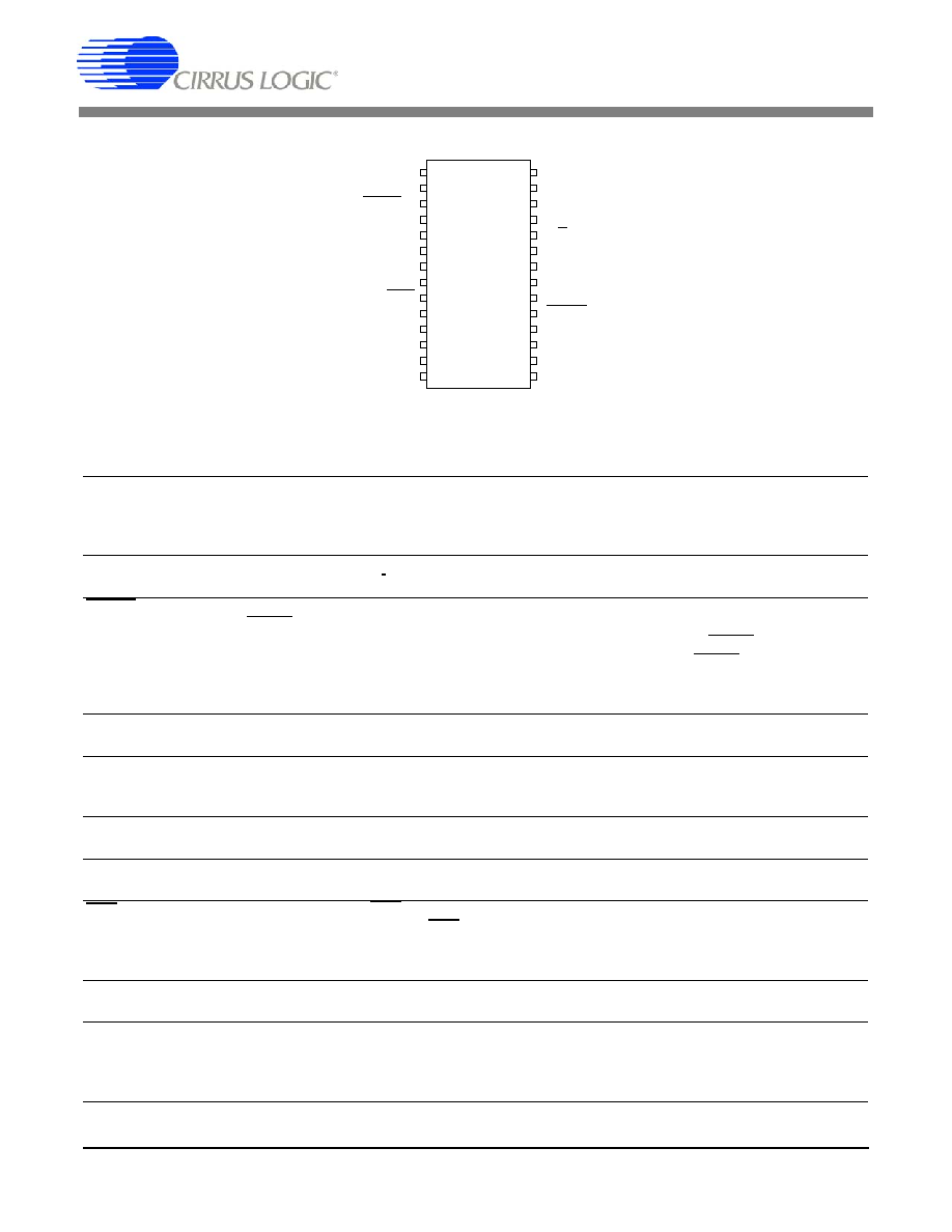
CS8427
44
DS477F3
14. PIN DESCRIPTION - HARDWARE MODE
* Pins which remain the same function in all modes.
+ Pins which require a pull up or pull down resistor
to select the desired startup option.
COPY
DGND2
EMPH/U
RXP
RXN
VA+
AGND
FILT
RST
RMCK
RERR
ILRCK
ISCLK
SDIN
+28
27
*26
*25
*24
*23
*22
21
20
19
+*18
*17
*16
*15
1+
2
3
4*
5*
6*
7*
8*
9*
10*+
11*+
12*
13*
14*
ORIG
V 2+
TXP
TXN
H/S
V +
DGND
APMS
PRO/C
AUDIO/V
SDOUT
OLRCK
OSCLK
TCBL
L
L
COPY
1
COPY Channel Status Bit (Output) - Reflects the state of the Copyright Channel Status bit in
the incoming AES3 data stream. If the category code is set to General, copyright will be indi-
cated whatever the state of the Copyright bit. This is also a start-up option pin, and requires a
pull-up or pull-down resistor.
DGND2
DGND
2
22
Digital Ground (Input) - Ground for the digital section. DGND should be connected to the
same ground as AGND.
EMPH/U
3
Pre-Emphasis Indicator / U-bit (Input/Output) - The EMPH/U pin either reflects the state of
the EMPH channel status bit in the incoming AES3 data stream, or is the serial U-bit input for
the AES3 transmitted data, clocked by OLRCK. If indicating emphasis: EMPH/U is low when
the incoming Channel Status data indicates 50/15 ms pre-emphasis. EMPH/U is high when
the Channel Status data indicates no pre-emphasis or indicates pre-emphasis other than
50/15 ms.
RXP
RXN
4
5
Differential Line Receiver (Input) - Receives differential AES3 data.
VA+
6
Positive Analog Power (Input) - Positive supply for the analog section. Nominally +5.0 V.
This supply should be as quiet as possible since noise on this pin will directly affect the jitter
performance of the recovered clock
AGND
7
Analog Ground (Input) - Ground for the analog section. AGND should be connected to the
same ground as DGND
FILT
8
PLL Loop Filter (Output) - An RC network should be connected between this pin and ground.
See "Appendix C: PLL Filter" on page 54 for recommended schematic and component values.
RST
9
Reset (Input) - When RST is low, the CS8427 enters a low power mode and all internal states
are reset. On initial power up, RST must be held low until the power supply is stable, and all
input clocks are stable in frequency and phase. This is particularly true in hardware mode with
multiple CS8427 devices where synchronization between devices is important
RMCK
10 Input Section Recovered Master Clock (Output) - Input section recovered master clock out-
put when PLL is used. Frequency is 256x the sample rate (Fs).
RERR
11
Receiver Error (Output) - When high, indicates an error in the operation of the AES3 receiver.
The status of this pin is updated once per sub-frame of incoming AES3 data. Conditions that
can cause RERR to go high are: parity error, bi-phase coding error, confidence, as well as loss
of lock by the PLL.
CS8427
DS477F3
45
ILRCK
12 Serial Audio Input Left/Right Clock (Input/Output) - Word rate clock for the audio data on
the SDIN pin.
ISCLK
13 Serial Audio Bit Clock (Input/Output) - Serial bit clock for audio data on the SDIN pin.
SDIN
14 Serial Audio Data Port (Input) - Audio data serial input pin.
TCBL
15 Transmit Channel Status Block Start (Input/Output) - When operated as output, TCBL is
high during the first sub-frame of a transmitted channel status block, and low at all other times.
When operated as input, driving TCBL high for at least three OMCK clocks will cause the next
transmitted sub-frame to be the start of a channel status block.
OSCLK
16 Serial Audio Output Bit Clock (Input/Output) - Serial bit clock for audio data on the SDOUT
pin
OLRCK
17 Serial Audio Output Left/Right Clock (Input/Output) - Word rate clock for the audio data on
the SDOUT pin. Frequency will be the output sample rate (Fs)
SDOUT
18 Serial Audio Output Data (Output) - Audio data serial output pin
AUDIO/V
19 Audio Channel Status Bit / V-Bit (Input/Output) - Reflects either the state of the audio/non-
audio Channel Status bit in the incoming AES3 data stream or is the Validity bit data input for
the AES3 transmitted data stream, clocked by OLRCK.
PRO/C
20 PRO Channel Status Bit / C-Bit (Input/Output) - Reflects either the state of the Profes-
sional/Consumer Channel Status bit in the incoming AES3 data stream or is the serial C-bit
input for the AES3 transmitted data, clocked by OLRCK.
APMS
21 Serial Audio Input Port Master/Slave Select (Input) - APMS should be connected to VL+ to
set serial audio input port as a master, or connected to DGND to set the port as a slave.
VL+
VL2+
23
27
Positive Digital Power (Input) - Typically +3.3 V or +5.0 V.
H/S
24 Hardware/Software Mode Control (Input) - Determines the method of controlling the opera-
tion of the CS8427, and the method of accessing CS and U data. In software mode, device
control and CS and U data access is primarily through the control port, using a microcontroller.
Hardware mode provides an alternate mode of operation and access to the CS and U data
through dedicated pins.
This pin should be permanently tied to VL+ or DGND
TXP
TXN
25
26
Differential Line Driver (Output) - Drivers transmit AES3 data and are pulled low while the
CS8427 is in the reset state.
ORIG
28 ORIG Channel Status Bit (Output) - SCMS generation indicator. This is decoded from the
incoming category code and the L bit. A low output indicates that the source of the audio data
stream is a copy. A high indicates that the source of the audio data stream is an original
recording. This is also a start-up option pin, and requires a pull-up or pull-down resistor.

CS8427
46
DS477F3
15. APPLICATIONS
15.1 Reset, Power Down and Start-up
When RST is low, the CS8427 enters a low power
mode and all internal states are reset, including the
control port and registers, and the outputs are mut-
ed. When RST is high, the control port becomes
operational and the desired settings should be
loaded into the control registers. Writing a 1 to the
RUN bit will then cause the part to leave the low
power state and begin operation. After the PLL has
settled, the AES3 and serial audio outputs will be
enabled.
Some options within the CS8427 are controlled by
a start-up mechanism. During the reset state,
some of the output pins are reconfigured internally
to be inputs. Immediately upon exiting the reset
state, the level of these pins is sensed. The pins
are then switched to be outputs. This mechanism
allows output pins to be used to set alternative
modes in the CS8427 by connecting a 47 k
resis-
tor to between the pin and either VL+ (HI) or DGND
(LO). For each mode, every start-up option select
pin MUST have an external pull-up or pull-down re-
sistor. In software mode, the only start-up option
pin is EMPH, which is used to set a chip address
bit for the control port in I≤C mode. Hardware
modes use many start-up options, which are de-
tailed in the hardware definition section at the end
of this data sheet.
15.2 ID Code and Revision Code
The CS8427 has a register that contains a four bit
code to indicate that the addressed device is a
CS8427. This is useful when other CS84XX family
members are resident in the same system, allow-
ing common software modules.
The CS8427 four bit revision code is also avail-
able. This allows the software driver for the
CS8427 to identify which revision of the device is
in a particular system, and modify its behavior ac-
cordingly. To allow for future revisions, it is strongly
recommend that the revision code is read into a
variable area within the microcontroller, and used
wherever appropriate as revision details become
known.
15.3 Power Supply, Grounding, and PCB
layout
For most applications, the CS8427 can be operat-
ed from a single +5.0 V supply, following normal
supply decoupling practices, see
Figure 5 on page
11
. Note that the I≤C protocol is supported only in
VL+ = 5.0 V mode. For applications where the re-
covered input clock, output on the RMCK pin, is re-
quired to be low jitter, then use a separate, quiet,
analog +5.0 V supply for VA+, decoupled to
AGND. In addition, a separate region of analog
ground plane around the FILT, AGND, VA+, RXP,
and RXN pins is recommended.
The VL+ supply should be well decoupled with a
0.1
µ
F capacitor to DGND to minimize AES3 trans-
mitter induced transients.
Extensive use of power and ground planes, ground
plane fill in unused areas and surface mount de-
coupling capacitors are recommended. Decou-
pling capacitors should be mounted on the same
side of the board as the CS8427 to minimize induc-
tance effects, and all decoupling capacitors should
be as close to the CS8427 as possible.
15.4 Synchronization of Multiple
CS8427s
The serial audio output ports of multiple CS8427s
can be synchronized if all devices share the same
master clock, OSCLK, OLRCK, and RST line and
leave the reset state on the same master clock fall-
ing edge. Either all the ports need to be in slave
mode, or one can be set as a master.
Multiple AES3 transmitters can be synchronized if
all devices share the same master clock, TCBL,
and RST signals and leave the reset state on the
same master clock falling edge. The TCBL pin is
used to synchronize multiple CS8427 AES3 trans-
mitters at the channel status block boundaries.
One CS8427 must have its TCBL set to master;
the others must be set to slave TCBL. Alternative-
ly, TCBL can be derived from external logic, in
which case all the CS8427 devices should be set
to slave TCBL.
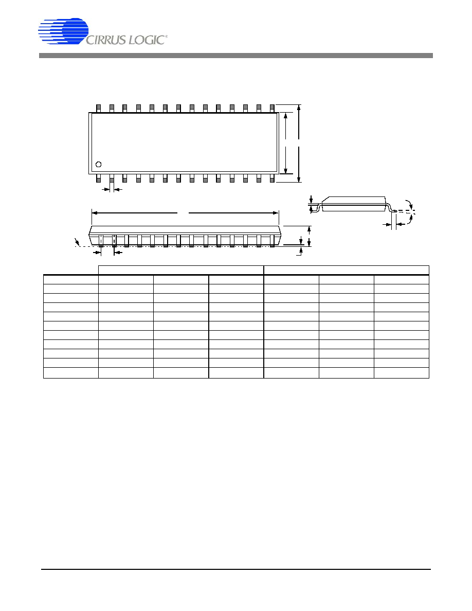
CS8427
DS477F3
47
16. PACKAGE DIMENSIONS
INCHES
MILLIMETERS
DIM
MIN
NOM
MAX
MIN
NOM
MAX
A 0.093
0.098
0.104
2.35
2.50
2.65
A1
0.004
0.008
0.012
0.10
0.20
0.30
b
0.013
0.017
0.020
0.33
0.42
0.51
C
0.009
0.011
0.013
0.23
0.28
0.32
D
0.697
0.705
0.713
17.70
17.90
18.10
E
0.291
0.295
0.299
7.40
7.50
7.60
e
0.040
0.050
0.060
1.02
1.27
1.52
H
0.394
0.407
0.419
10.00
10.34
10.65
L
0.016
0.026
0.050
0.40
0.65
1.27
0∞
4∞
8∞
0∞
4∞
8∞
JEDEC #: MS-013
Controlling Dimension is Millimeters
28L SOIC (300 MIL BODY) PACKAGE DRAWING
D
H
E
b
A1
A
c
L
SEATING
PLANE
1
e

CS8427
48
DS477F3
Notes: 1. "D" and "E1" are reference datums and do not included mold flash or protrusions, but do include mold
mismatch and are measured at the parting line, mold flash or protrusions shall not exceed 0.20 mm per
side.
2. Dimension "b" does not include dambar protrusion/intrusion. Allowable dambar protrusion shall be
0.13 mm total in excess of "b" dimension at maximum material condition. Dambar intrusion shall not
reduce dimension "b" by more than 0.07 mm at least material condition.
3. These dimensions apply to the flat section of the lead between 0.10 and 0.25 mm from lead tips.
INCHES
MILLIMETERS
NOTE
DIM
MIN
NOM
MAX
MIN
NOM
MAX
A
--
--
0.47
--
--
1.20
A1
0.002
0.004
0.006
0.05
0.10
0.15
A2
0.03150
0.035
0.04
0.80
0.90
1.00
b
0.00748
0.0096
0.012
0.19
0.245
0.30
2,3
D
0.378 BSC
0.382 BSC
0.386 BSC
9.60 BSC
9.70 BSC
9.80 BSC
1
E
0.248
0.2519
0.256
6.30
6.40
6.50
E1
0.169
0.1732
0.177
4.30
4.40
4.50
1
e
--
0.026 BSC
--
--
0.65 BSC
--
L
0.020
0.024
0.029
0.50
0.60
0.75
0∞
4∞
8∞
0∞
4∞
8∞
JEDEC #: MO-153
Controlling Dimension is Millimeters.
28L TSSOP (4.4 mm BODY) PACKAGE DRAWING
E
N
1 2 3
e
b
2
A1
A2
A
D
SEATING
PLANE
E1
1
L
SIDE VIEW
END VIEW
TOP VIEW

CS8427
DS477F3
49
17. APPENDIX A: EXTERNAL
AES3/SPDIF/IEC60958 TRANSMITTER
AND RECEIVER COMPONENTS
This section details the external components re-
quired to interface the AES3 transmitter and re-
ceiver to cables and fiber-optic components.
17.1 AES3 Transmitter External
Components
The output drivers on the CS8427 are designed to
drive both the professional and consumer interfac-
es. The AES3 specification for professional/broad-
cast use calls for a 110
source impedance and a
balanced drive capability. Since the transmitter
output impedance is very low, a 110
resistor
should be placed in series with one of the transmit
pins. The specifications call for a balanced output
drive of 2-7 V peak-to-peak into a 110
load with
no cable attached. Using the circuit in
Figure 20
,
the output of the transformer is short-circuit pro-
tected, has the proper source impedance, and pro-
vides a 5 V peak-to-peak signal into a 110
load.
Lastly, the two output pins should be attached to
an XLR connector with male pins and a female
shell, and with pin 1 of the connector grounded.
In the case of consumer use, the IEC60958 speci-
fications call for an unbalanced drive circuit with an
output impedance of 75
and a output drive level
of 0.5 V peak-to-peak ±20% when measured
across a 75
load using no cable. The circuit
shown in Figure 21 only uses the TXP pin and pro-
vides the proper output impedance and drive level
using standard 1% resistors. If VL+ is driven from
+3.3 V, use resistor values of 243
and 107
.
The connector for a consumer application would
be an RCA phono socket. This circuit is also short
circuit protected.
The TXP pin may be used to drive TTL or CMOS
gates as shown in Figure 22. This circuit may be
used for optical connectors for digital audio since
they usually have TTL or CMOS compatible inputs.
This circuit is also useful when driving multiple dig-
ital audio outputs since RS422 line drivers have
TTL compatible inputs.
17.2 Isolating Transformer Requirements
Please refer to the application note AN134: AES
and SPDIF Recommended Transformers for re-
sources on transformer selection.
110-(R
TXP
+R
TXN
)
TXP
TXN
XLR
1
CS8427
Figure 20. Professional Output Circuit
Figure 21. Consumer Output Circuit
374-R
TXP
90.9
TXP
TXN
RCA
Phono
CS8427
Figure 22. TTL/CMOS Output Circuit
TXP
TXN
TTL or
CMOS Gate
CS8427

CS8427
50
DS477F3
17.3 AES3 Receiver External
Components
The CS8427 AES3 receiver is designed to accept
both the professional and consumer interfaces.
The digital audio specifications for professional
use call for a balanced receiver, using XLR con-
nectors, with 110
±20% impedance. The XLR
connector on the receiver should have female pins
with a male shell. Since the receiver has a very
high input impedance, a 110
resistor should be
placed across the receiver terminals to match the
line impedance, as shown in
Figure 23
. Although
transformers are not required by the AES, they are,
however, strongly recommended.
If some isolation is desired without the use of trans-
formers, a 0.01
µ
F capacitor should be placed in
series with each input pin (RXP and RXN) as
shown in
Figure 24
. However, if a transformer is
not used, high frequency energy could be coupled
into the receiver, causing degradation in analog
performance.
Figure 23
and
Figure 24
show an optional DC
blocking capacitor (0.1
µ
F to 0.47
µ
F) in series
with the cable input. This improves the robustness
of the receiver, preventing the saturation of the
transformer, or any DC current flow, if a DC voltage
is present on the cable.
In the configuration of systems, it is important to
avoid ground loops and DC current flowing down
the shield of the cable that could result when boxes
with different ground potentials are connected.
Generally, it is good practice to ground the shield
to the chassis of the transmitting unit, and connect
the shield through a capacitor to chassis ground at
the receiver. However, in some cases it is advan-
tageous to have the ground of two boxes held to
the same potential, and the cable shield might be
depended upon to make that electrical connection.
Generally, it may be a good idea to provide the op-
tion of grounding or capacitively coupling the shield
to the chassis.
In the case of the consumer interface, the stan-
dards call for an unbalanced circuit having a re-
ceiver impedance of 75
±5%. The connector for
the consumer interface is an RCA phono socket.
The receiver circuit for the consumer interface is
shown in
Figure 25
.
The circuit shown in
Figure 26
may be used when
external RS422 receivers, optical receivers or oth-
er TTL/CMOS logic outputs drive the CS8427 re-
ceiver section.
17.4 Isolating Transformer Requirements
Please refer to the application note AN134: "AES
and SPDIF Recommended Transformers" for re-
sources on transformer selection
1
XLR
Twisted
Pair
110
110
CS8427
RXP
RXN
0.01 F
µ
0.01 F
µ
* See Text
Figure 23. Professional Input Circuit
Figure 24. Transformerless Professional Input Circuit
1
XLR
Twisted
Pair
110
110
CS8427
RXP
RXN
0.01 F
µ
0.01 F
µ
* See Text
RCA Phono
RXP
RXN
CS8427
Coax
75
75
0.01 F
µ
0.01 F
µ
Figure 25. Consumer Input Circuit
Figure 26. TTL/CMOS Input Circuit
RXP
RXN
CS8427
0.01 F
µ
0.01 F
µ
TTL/CMOS
Gate
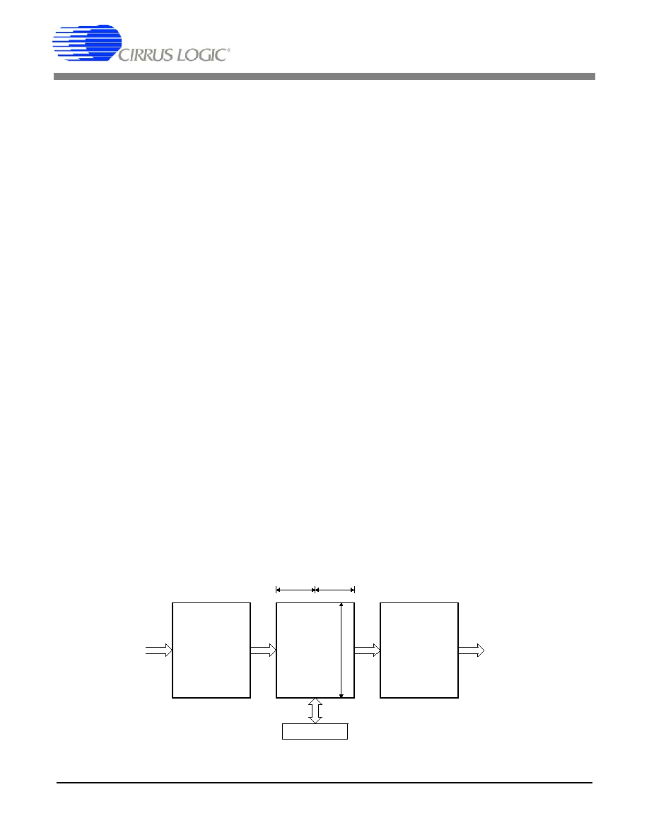
CS8427
DS477F3
51
18. APPENDIX B: CHANNEL STATUS AND
USER DATA BUFFER MANAGEMENT
The CS8427 has a comprehensive channel status
(C) and user (U) data buffering scheme, which al-
lows automatic management of channel status
blocks and user data. Alternatively, sufficient con-
trol and access is provided to allow the user to
completely manage the C and U data through the
control port. Be aware that the RUN bit should be
set to 1 in order to access the C and U data buffer
through the control port.
18.1 AES3 Channel Status(C) Bit
Management
The CS8427 contains sufficient RAM to store a full
block of C data for both A and B channels (192x2
= 384 bits), and also 384 bits of U information. The
user may read from or write to these RAMs through
the control port.
The CS8427 manages the flow of channel status
data at the block level, meaning that entire blocks
of channel status information are buffered at the in-
put, synchronized to the output timebase, and then
transmitted. The buffering scheme involves a cas-
cade of 3 block-sized buffers, named D,E and F, as
shown in
Figure 27
. The MSB of each byte repre-
sents the first bit in the serial C data stream. For
example, the MSB of byte 0 (which is at control port
address 20h) is the consumer/professional bit for
channel status block A.
The first buffer, D, accepts incoming C data from
the AES receiver. The 2nd buffer, E, accepts entire
blocks of data from the D buffer. The E buffer is
also accessible from the control port, allowing read
and writing of the C data. The 3rd buffer (F) is used
as the source of C data for the AES3 transmitter.
The F buffer accepts block transfers from the E
buffer.
18.1.1 Manually accessing the E buffer
The user can monitor the data being transferred by
reading the E buffer, which is mapped into the reg-
ister space of the CS8427, through the control port.
The user can modify the data to be transmitted by
writing to the E buffer.
The user can configure the interrupt enable regis-
ter to cause interrupts to occur whenever "D to E"
or "E to F" buffer transfers occur. This allows deter-
mination of the allowable time periods to interact
with the E buffer.
Also provided are "D to E" and "E to F" inhibit bits.
The associated buffer transfer is disabled whenev-
er the user sets these bits. These may be used
whenever "long" control port interactions are oc-
curring. They can also be used to align the behav-
ior of the buffers with the selected audio data flow.
For example, if the audio data flow is serial port in
to AES3 out, then it is necessary to inhibit "D toE"
transfers, since these would overwrite the desired
transmit C data with invalid data.
Flowcharts for reading and writing to the E buffer
are shown in
Figure 28
and
Figure 29
. For reading,
since a D to E interrupt just occurred, then there a
substantial time interval until the next D to E trans-
fer (approximately 24 frames worth of time). This is
usually plenty of time to access the E data without
having to inhibit the next transfer.
Control Port
From
AES3
Receiver
To
AES3
Transmitter
E
24
words
8-bits
8-bits
A
B
D
F
Received
Data
Buffer
Transmit
Data
Buffer
Figure 27. Channel Status Data Buffer Structure

CS8427
52
DS477F3
For writing, the sequence starts after a E to F trans-
fer, which is based on the output timebase. Since
a D to E transfer could occur at any time (this is
based on the input timebase), then it is important
to inhibit D to E transfers while writing to the E buff-
er until all writes are complete. Then wait until the
next E to F transfer occurs before enabling D to E
transfers. This ensures that the data written to the
E buffer actually gets transmitted and not overwrit-
ten by a D to E transfer.
If the channel status block to transmit indicates
PRO mode, then the CRCC byte is automatically
calculated by the CS8427, and does not have to be
written into the last byte of the block by the host mi-
crocontroller.
18.1.2 Reserving the first 5 bytes in the E
buffer
D to E buffer transfers periodically overwrite the
data stored in the E buffer. This can be a problem
for users who want to transmit certain channel sta-
tus settings which are different from the incoming
settings. In this case, the user would have to su-
perimpose his settings on the E buffer after every
D to E overwrite.
To avoid this problem, the CS8427 has the capa-
bility of reserving the first 5 bytes of the E buffer for
user writes only. When this capability is in use, in-
ternal D to E buffer transfers will NOT affect the
first 5 bytes of the E buffer. Therefore, the user can
set values in these first 5 E bytes once, and the set-
tings will persist until the next user change. This
mode is enabled by the Channel Status Data Buff-
er Control register.
18.1.3 Serial Copy Management System
(SCMS)
In software mode, the CS8427 allows read/modi-
fy/write access to all the channel status bits. For
consumer mode SCMS compliance, the host mi-
crocontroller needs to read and manipulate the
Category Code, Copy bit and L bit appropriately.
In hardware mode, the SCMS protocol can be fol-
lowed by either using the COPY and ORIG input
pins, or by using the C bit serial input pin. These
options are documented in the hardware mode
section of this data sheet.
18.1.4 Channel Status Data E Buffer
Access
The E buffer is organized as 24 x 16-bit words. For
each word the MS Byte is the A channel data, and
the LS Byte is the B channel data (see
Figure 27
).
There are two methods of accessing this memory,
known as one byte mode and two byte mode. The
desired mode is selected through a control register
bit.
One Byte Mode
In many applications, the channel status blocks for
the A and B channels will be identical. In this situ-
ation, if the user reads a byte from one of the chan-
nel's blocks, the corresponding byte for the other
channel will be the same. Similarly, if the user
wrote a byte to one channel's block, it would be
necessary to write the same byte to the other
block. One byte mode takes advantage of the often
identical nature of A and B channel status data.
Figure 28. Flowchart for Reading the E Buffer
D to E interrupt occurs
Optionally set D to E inhibit
Read E data
If set, clear D to E inhibit
Return
E to F interrupt occurs
Optionally set E to F inhibit
Clear D to E inhibit
If set, clear E to F inhibit
Return
Set D to E inhibit
Write E data
Wait for E to F transfer
Figure 29. Flowchart for Writing the E Buffer

CS8427
DS477F3
53
When reading data in one byte mode, a single byte
is returned, which can be from channel A or B data,
depending on a register control bit. If a write is be-
ing done, the CS8427 expects a single byte to be
input to its control port. This byte will be written to
both the A and B locations in the addressed word.
One byte mode saves the user substantial control
port access time, as it effectively accesses 2 bytes
worth of information in 1 byte's worth of access
time. If the control port's autoincrement addressing
is used in combination with this mode, multi-byte
accesses such as full-block reads or writes can be
done especially efficiently.
Two Byte mode
There are those applications in which the A and B
channel status blocks will not be the same, and the
user is interested in accessing both blocks. In
these situations, two byte mode should be used to
access the E buffer.
In this mode, a read will cause the CS8427 to out-
put two bytes from its control port. The first byte out
will represent the A channel status data, and the
2nd byte will represent the B channel status data.
Writing is similar, in that two bytes must now be in-
put to the CS8427's control port. The A channel
status data is first, B channel status data second.
18.2 AES3 User (U) Bit Management
The CS8427 U bit manager has two operating
modes: transmit all zeros and block mode.
18.2.1 Mode 1: Transmit All Zeros
Mode 1 causes only zeros to be transmitted in the
output U data, regardless of E buffer contents or
U data embedded in an input AES3 data stream.
This mode is intended for the user who does not
want to transceive U data, and simply wants the
output U channel to contain no data.
18.2.2 Mode 2: Block Mode
Mode 2 is very similar to the scheme used to con-
trol the C bits. Entire blocks of U data are buffered
from input to output, using a cascade of 3 block-
sized RAMs to perform the buffering. The user has
access to the second of these 3 buffers, denoted
the E buffer, through the control port. Block mode
is designed for use in AES3 in, AES3 out situations
in which input U data is decoded using a microcon-
troller through the control port. It is also the only
mode in which the user can merge his own U data
into the transmitted AES3 data stream.
The U buffer access only operates in two byte
mode, since there is no concept of A and B blocks
for user data. The arrangement of the data is as fol-
lows:Bit15[A7]Bit14[B7]Bit13[A6]Bit12[B6]...Bit1[A
0]Bit0[B0]. The arrangement of the data in the
each byte is that the MSB is the first received bit
and is the first transmitted bit. The first byte read is
the first byte received, and the first byte sent is the
first byte transmitted. If you read two bytes from the
E buffer, you will get the following arrangement:
A[7]B[7]A[6]B[6]....A[0]B[0].

CS8427
54
DS477F3
19. APPENDIX C: PLL FILTER
19.1 General
An on-chip Phase Locked Loop (PLL) is used to re-
cover the clock from the incoming data stream.
Figure 30 is a simplified diagram of the PLL in
these parts. When the PLL is locked to an AES3 in-
put stream, it is updated at each preamble in the
AES3 stream. This occurs at twice the sampling
frequency, F
S
. When the PLL is locked to ILRCK,
it is updated at F
S
so that the duty cycle of the input
doesn't affect jitter.
There are some applications where low jitter in the
recovered clock, presented on the RMCK pin, is
important. For this reason, the PLL has been de-
signed to have good jitter attenuation characteris-
tics, as shown in Figure 33, Figure 34, Figure 35,
and Figure 36. In addition, the PLL has been de-
signed to only use the preambles of the AES3
stream to provide lock update information to the
PLL. This results in the PLL being immune to data
dependent jitter affects because the AES3 pream-
bles do not vary with the data.
The PLL has the ability to lock onto a wide range of
input sample rates with no external component
changes. If the sample rate of the input subse-
quently changes, for example in a varispeed appli-
cation, the PLL will only track up to ±12.5% from
the nominal center sample rate. The nominal cen-
ter sample rate is the sample rate that the PLL first
locks onto upon application of an AES3 data
stream or after enabling the CS8427 clocks by set-
ting the RUN control bit. If the 12.5% sample rate
limit is exceeded, the PLL will return to its wide lock
range mode and re-acquire a new nominal center
sample rate.
Phase
Comparator
and Charge Pump
˜
N
VCO
RMCK
INPUT
Crip
Cfilt
Rfilt
Figure 30. PLL Block Diagram
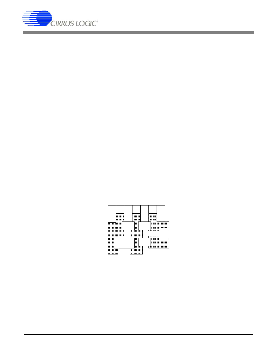
CS8427
DS477F3
55
19.2 External Filter Components
19.2.1 General
The PLL behavior is affected by the external filter
component values. Figure 5 on page 11 shows the
recommended configuration of the two capacitors
and one resistor that comprise the PLL filter. In
Table 7 and Table 8, the component values shown
for the 32 to 96 kHz range have the highest corner
frequency jitter attenuation curve, takes the short-
est time to lock, and offers the best output jitter per-
formance. The component values shown in
Table 6 and Table 8 for the 8 to 96 kHz range al-
lows the lowest input sample rate to be 8 kHz, and
increases the lock time of the PLL. Lock times are
worst case for an Fsi transition of 96 kHz.
19.2.2 Capacitor Selection
The type of capacitors used for the PLL filter can
have a significant effect on receiver performance.
Large or exotic film capacitors are not necessary
as their leads and the required longer circuit board
traces add undesirable inductance to the circuit.
Surface mount ceramic capacitors are a good
choice because their own inductance is low, and
they can be mounted close to the FILT pin to
minimize trace inductance. For C
RIP
, a C0G or
NPO dielectric is recommended, and for C
FILT
, an
X7R dielectric is preferred. Avoid capacitors with
large temperature coefficients, or capacitors with
high dielectric constants, that are sensitive to
shock and vibration. These include the Z5U and
Y5V dielectrics.
19.2.3 Circuit Board Layout
Board layout and capacitor choice affect each
other and determine the performance of the PLL.
Figure 31 contains a suggested layout for the PLL
filter components and for bypassing the analog
supply voltage. The 0.1 µF bypass capacitor is in a
1206 form factor. R
FILT
and the other three
capacitors are in an 0805 form factor. The traces
are on the top surface of the board with the IC so
that there is no via inductance. The traces
themselves are short to minimize the inductance in
the filter path. The VA+ and AGND traces extend
back to their origin and are shown only in truncated
form in the drawing.
VA+
AGND
FILT
Cfilt
1000
pF
.1µF
R
fil
t
Crip
Figure 31. Recommended Layout Example
CS8427
56
DS477F3
19.3 Component Value Selection
When transitioning from one revision of the part
another, component values may need to be
changed. While it is mandatory for customers to
change the external PLL component values when
transitioning from revision A to revision A1 or from
revision A to revision A2, customers do not need to
change external PLL component values when tran-
sitioning from revision A1 to revision A2, unless the
part is used in an application that is required to
pass the AES3 or IEC60958-4 specification for re-
ceiver jitter tolerance (see Table 7).
19.3.1 Identifying the Part Revision
The first line of the part marking on the package in-
dicates the part number and package type
(CS8427-xx). Table 5 shows a list of part revisions
and their corresponding second line part marking,
which indicates what revision the part is.
19.3.2 Locking to the RXP/RXN Receiver
Inputs
CS8427 parts that are configured to lock to only
the RXP/RXN receiver inputs should use the exter-
nal PLL component values listed in Table 6 and
Table 7. Values listed for the 32 to 96 kHz Fs
range will have the highest corner frequency jitter
attenuation curve, take the shortest time to lock,
and offer the best output jitter performance.
Revision
Pre-October 2002
SOIC & TSSOP (10-Digit)
New SOIC
(12-Digit)
New TSSOP
(10-Digit)
A
Zxxxxxxxxx
ZFBAAXxxxxxx
NAAXxxxxxx
A1
Rxxxxxxxxx
RFBAA1xxxxxx
NAA1xxxxxx
A2
N/A
RFBAA2xxxxxx
NAA2xxxxxx
Table 5. Second Line Part Marking
Revision
R
FILT
(k
)
C
FILT
(
µ
F)
C
RIP
(nF)
PLL Lock Time (ms)
A
0.909
1.8
33
56
A1
0.4
0.47
47
60
A2
0.4
0.47
47
60
Table 6. Locking to RXP/RXN - Fs = 8 to 96 kHz
Revision
R
FILT
(k
)
C
FILT
(
µ
F)
C
RIP
(nF)
PLL Lock Time (ms)
A*
3.0
0.047
2.2
35
A1*
1.2
0.1
4.7
35
A2
1.2
0.1
4.7
35
A2*
1.6
0.33
4.7
35
Table 7. Locking to RXP/RXN - Fs = 32 to 96 kHz
* Parts used in applications that are required to pass the AES3 or IEC60958-4 specification for re-
ceiver jitter tolerance should use these component values. Please note that the AES3 and IEC60958
specifications do not have allowances for locking to sample rates less than 32 kHz or for locking to
the ILRCK input. Also note that many factors can affect jitter performance in a system. Please follow
the circuit and layout recommendations outlined previously.
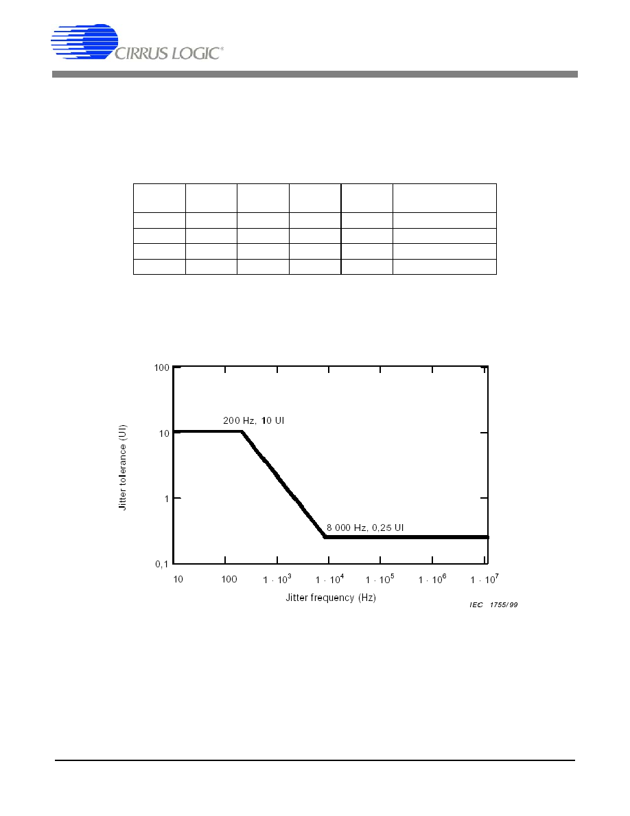
CS8427
DS477F3
57
19.3.3 Locking to the ILRCK Input
CS8427 parts that are configured to lock to the IL-
RCK input should use the external PLL component
values listed in Table 8. Note that parts that need
to lock to both ILRCK and RXP/RXN should use
these values. Values listed for the 32 to 96 kHz Fs
range will have the highest corner frequency jitter
attenuation curve, take the shortest time to lock,
and offer the best output jitter performance.
19.3.4 Jitter Tolerance
Shown in Figure 32 is the Receiver Jitter Tolerance
template as illustrated in the AES3 and IEC60958-
4 specification. CS8427 parts used with the appro-
priate external PLL component values (as noted in
Table 7) have been tested to pass this template.
Revision
Fs Range
(kHz)
R
FILT
(k
) C
FILT
(
µ
F) C
RIP
(nF) PLL Lock Time (ms)
A
8 to 96
1.3
2.7
62
120
A
32-96
5.1
0.15
3.9
70
A1/A2
8 to 96
0.3
1.0
100
120
A1/A2
32-96
0.6
0.22
22
70
Table 8. Locking to the ILRCK Input
Figure 32. Jitter Tolerance Template

CS8427
58
DS477F3
19.3.5 Jitter Attenuation
Shown in Figure 33, Figure 34, Figure 35, and Fig-
ure 36 are jitter attenuation plots for the various re-
visions of the CS8427 when used with the
appropriate external PLL component values (as
noted in Table 7). The AES3 and IEC60958-4
specifications do not have allowances for locking
to sample rates less than 32 kHz or for locking to
the ILRCK input. These specifications state a max-
imum of 2 dB jitter gain or peaking.
10
-1
10
0
10
1
10
2
10
3
10
4
10
5
-20
-15
-10
-5
0
5
Jitter Frequency (Hz)
Jitter Attenuation (dB)
10
-1
10
0
10
1
10
2
10
3
10
4
10
5
-20
-15
-10
-5
0
5
Jitter Frequency (Hz)
Jitter Attenuation (dB)
10
-1
10
0
10
1
10
2
10
3
10
4
10
5
-25
-20
-15
-10
-5
0
5
Jitter Frequency (Hz)
Jitter Attenuation (dB)
10
-1
10
0
10
1
10
2
10
3
10
4
10
5
-25
-20
-15
-10
-5
0
5
Jitter Frequency (Hz)
Jitter Attenuation (dB)
Figure 33. Revision A
Figure 34. Revision A1
Figure 35. Revision A2 using A1 values
Figure 36. Revision A2 using A2* values

CS8427
DS477F3
59
20. REVISION HISTORY
Release
Date
Changes
PP1
November 1999
1st Preliminary Release
PP2
November 2000
2nd Preliminary Release
PP3
May 2001
3rd Preliminary Release
PP4
February 2003
4th Preliminary Release
F1
January 2004
Final Release
Updated "Appendix C: PLL Filter" on page 54 to include information from errata
ER477E2
F2
July 2004
Add lead free ordering information
F3
January 2005
-Changed format of Figures 15 and 16 on page 23 and page 24.
-Corrected AES3 Direct format in figure 16 on page 24 and text reference to
AES3 Direct format on page 15.
-Changed description of DETC, EFTC, DETU,and EFTU bits in "Control Port
Register Bit Definitions" on page 32 and page 33.
Table 9. Revision History
Contacting Cirrus Logic Support
For all product questions and inquiries contact a Cirrus Logic Sales Representative.
To find the one nearest to you go to
www.cirrus.com
IMPORTANT NOTICE
Cirrus Logic, Inc. and its subsidiaries ("Cirrus") believe that the information contained in this document is accurate and reliable. However, the information is subject
to change without notice and is provided "AS IS" without warranty of any kind (express or implied). Customers are advised to obtain the latest version of relevant
information to verify, before placing orders, that information being relied on is current and complete. All products are sold subject to the terms and conditions of sale
supplied at the time of order acknowledgment, including those pertaining to warranty, indemnification, and limitation of liability. No responsibility is assumed by Cirrus
for the use of this information, including use of this information as the basis for manufacture or sale of any items, or for infringement of patents or other rights of third
parties. This document is the property of Cirrus and by furnishing this information, Cirrus grants no license, express or implied under any patents, mask work rights,
copyrights, trademarks, trade secrets or other intellectual property rights. Cirrus owns the copyrights associated with the information contained herein and gives con-
sent for copies to be made of the information only for use within your organization with respect to Cirrus integrated circuits or other products of Cirrus. This consent
does not extend to other copying such as copying for general distribution, advertising or promotional purposes, or for creating any work for resale.
CERTAIN APPLICATIONS USING SEMICONDUCTOR PRODUCTS MAY INVOLVE POTENTIAL RISKS OF DEATH, PERSONAL INJURY, OR SEVERE PROP-
ERTY OR ENVIRONMENTAL DAMAGE ("CRITICAL APPLICATIONS"). CIRRUS PRODUCTS ARE NOT DESIGNED, AUTHORIZED OR WARRANTED FOR USE
IN AIRCRAFT SYSTEMS, MILITARY APPLICATIONS, PRODUCTS SURGICALLY IMPLANTED INTO THE BODY, AUTOMOTIVE SAFETY OR SECURITY DE-
VICES, LIFE SUPPORT PRODUCTS OR OTHER CRITICAL APPLICATIONS. INCLUSION OF CIRRUS PRODUCTS IN SUCH APPLICATIONS IS UNDER-
STOOD TO BE FULLY AT THE CUSTOMER'S RISK AND CIRRUS DISCLAIMS AND MAKES NO WARRANTY, EXPRESS, STATUTORY OR IMPLIED,
INCLUDING THE IMPLIED WARRANTIES OF MERCHANTABILITY AND FITNESS FOR PARTICULAR PURPOSE, WITH REGARD TO ANY CIRRUS PRODUCT
THAT IS USED IN SUCH A MANNER. IF THE CUSTOMER OR CUSTOMER'S CUSTOMER USES OR PERMITS THE USE OF CIRRUS PRODUCTS IN CRITICAL
APPLICATIONS, CUSTOMER AGREES, BY SUCH USE, TO FULLY INDEMNIFY CIRRUS, ITS OFFICERS, DIRECTORS, EMPLOYEES, DISTRIBUTORS AND
OTHER AGENTS FROM ANY AND ALL LIABILITY, INCLUDING ATTORNEYS' FEES AND COSTS, THAT MAY RESULT FROM OR ARISE IN CONNECTION
WITH THESE USES.
Cirrus Logic, Cirrus, and the Cirrus Logic logo designs are trademarks of Cirrus Logic, Inc. All other brand and product names in this document may be trademarks
or service marks of their respective owners.
SPI is a trademark of Motorola Inc.
AC-3 is a registered trademark of Dolby Laboratories Liscencing, Inc.