 | –≠–ª–µ–∫—Ç—Ä–æ–Ω–Ω—ã–π –∫–æ–º–ø–æ–Ω–µ–Ω—Ç: CL-PD6710 | –°–∫–∞—á–∞—Ç—å:  PDF PDF  ZIP ZIP |

CL-PD6710/'22
Preliminary Data Sheet
Æ
May 1997
Version 3.1
OVERVIEW
FEATURES
s
Single-chip PC Card host adapters
s
Direct connection to ISA (PC AT) bus and one or two
PC Card sockets
s
Compliant with PC Card Standard, PCMCIA 2.1, and
JEIDA 4.1
s
82365SL-compatible register set,
ExCA
TM
-compatible
s
Automatic Low-Power Dynamic mode for lowest
active power consumption
s
Programmable Suspend mode
s
Hardware-enabled Super Suspend mode
s
Five programmable memory windows per socket
and two programmable I/O windows per socket
s
Programmable card access cycle timing
s
8- or 16-bit system bus interface
s
8- and 16-bit PC Card interface support
s
ATA disk interface support
s
DMA support (CL-PD6722)
s
Card-voltage sense support
s
PC Card activity indicator
s
Mixed-voltage operation (3.3/5.0 V)
s
Single-socket interface: 144-pin VQFP for smallest
form factor (CL-PD6710)
s
Dual-socket interface: 208-pin PQFP or VQFP
(CL-PD6722)
The CL-PD6710 and CL-PD6722 are single-chip PC
Card host adapter solutions capable of controlling
one (CL-PD6710) or two (CL-PD6722) PC Card
sockets. The chips are compliant with PC Card Stan-
dard, PCMCIA 2.1, and JEIDA 4.1 and are optimized
for use in notebook and handheld computers where
reduced form factor and low power consumption are
critical design objectives. With the CL-PD6710, a
complete PC Card solution with power-control logic
can occupy less than 1.5 square inches (excluding
the socket connector). With the CL-PD6722, a com-
plete dual-socket PC Card solution with power-con-
trol logic can occupy less than 2 square inches
(excluding socket connectors).
The chips employ energy-efficient mixed-voltage
technology that can reduce system power consump-
tion by over 50 percent. The chips also provide: a
Low-Power Dynamic mode, which automatically
stops the internal clock during periods of card inac-
tivity; a software-controlled Suspend mode, which
dramatically reduces power by disabling most of the
internal circuitry and stopping data transactions to
the PC Cards; and a hardware-controlled Super Sus-
pend mode, which reduces current to the
µ
A range.
ISA≠to≠PC-Card Host Adapters
System
Block Diagram
ISA (AT)
BUS
PC CARD SOCKET 1
PC CARD SOCKET 2
CL-PD6710
144-Pin
...............................
...............................
PC Car
d
...............................
...............................
PC Car
d
(CL-PD6722)
CL-PD6722
208-Pin
(cont.)
PRELIMINARY DATA SHEET v3.1
CL-PD6710/'22
ISA≠to≠PC-Card Host Adapters
May 1997
2
The chips provide fully buffered PC Card interfaces,
meaning that no external logic is required for buffer-
ing signals to/from the interface, and power con-
sumption can be controlled by limiting signal
transitions on the PC Card bus.
Personal computer applications typically access PC
Cards through a third-party socket/card-services
software interface. To assure full compatibility with
industry-standard socket/card-services software and
PC Card applications, the register set in the
CL-PD6710 and CL-PD6722 is a superset of the
Intel
Æ
82365SL register set.
Notebook Computer Design Priorities
Supporting Features
s
Small Form Factor
Ã
Single-chip solutions
Ã
No external buffers for host or socket
Ã
Efficient board layout
s
Minimum Power Consumption
Ã
Automatic Low-Power Dynamic mode
Ã
Hardware- and software-controlled Suspend modes
Ã
Mixed-voltage operation
s
High Performance
Ã
Write cache
Ã
Programmable timing supports more cards, faster
reads and writes
Ã
Automatic bus sizing for 8- or 16-bit
Ã
DMA available with the CL-PD6722
s
Compatibility
Ã
Compliant with PC Card Standard, PCMCIA 2.1, and
JEIDA 4.1
Ã
82365SL A-step register-compatible,
ExCA
TM
-compatible
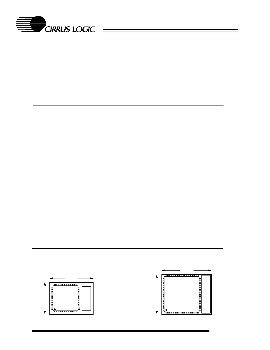
Host Adapter Form Factor
Card
1 3/8"
CL-PD6710
144-Pin VQFP
1"
VCC
VPP
and
Switch-
Cir-
CL-PD6722
208-Pin
ing
1 9/16"
1 1/4"
OVERVIEW
(cont.)
cuitry
Card
VCC
VPP
and
Switch-
Cir-
ing
cuitry
PQFP or VQFP

May 1997
3
PRELIMINARY DATA SHEET v3.1
CL-PD6710/'22
ISA≠to≠PC-Card Host Adapters
Table of Contents
1.
GENERAL CONVENTIONS.................. 7
2.
PIN INFORMATION ............................... 8
2.1
Pin Diagrams ..................................................... 9
2.2
Pin Description Conventions............................ 11
2.3
Pin Descriptions............................................... 12
2.4
Power-On Configuration Summary .................. 21
3.
INTRODUCTION.................................. 22
3.1
System Architecture......................................... 22
3.1.1
PC Card Basics ............................................ 22
3.1.2
CL-PD67XX Windowing Capabilities ............ 22
3.1.3
CL-PD67XX Functional Blocks ..................... 25
3.1.4
Interrupts ...................................................... 25
3.1.5
Alternate Functions of Interrupt Pins ............ 26
3.1.6
General-Purpose Strobe Feature ................. 26
3.1.7
Voltage Sense Pins....................................... 27
3.1.8
CL-PD67XX Power Management ................. 27
3.1.9
Socket Power Management Features........... 28
3.1.10 Write FIFO .................................................... 29
3.1.11 Bus Sizing..................................................... 29
3.1.12 Programmable PC Card Timing.................... 29
3.1.13 ATA Mode Operation..................................... 29
3.1.14 DMA Mode Operation for
the CL-PD6722............................................. 30
3.1.15 Selective Data Drive for I/O Windows ........... 30
3.2
Host Access to Registers................................. 30
3.3
Power-On Setup............................................... 31
4.
REGISTER DESCRIPTION
CONVENTIONS................................... 32
5.
OPERATION REGISTERS .................. 33
5.1
Index ................................................................ 33
5.2
Data ................................................................. 36
6.
CHIP CONTROL REGISTERS............ 37
6.1
Chip Revision................................................... 37
6.2
Interface Status................................................ 38
6.3
Power Control .................................................. 40
6.4
Interrupt and General Control .......................... 42
6.5
Card Status Change ........................................ 44
6.6
Management Interrupt Configuration ............... 45
6.7
Mapping Enable ............................................... 47
7.
I/O WINDOW MAPPING
REGISTERS ........................................ 49
7.1
I/O Window Control .......................................... 49
7.2
System I/O Map 0≠1 Start Address Low.......... 50
7.3
System I/O Map 0≠1 Start Address High......... 50
7.4
System I/O Map 0≠1 End Address Low ........... 51
7.5
System I/O Map 0≠1 End Address High .......... 51
7.6
Card I/O Map 0≠1 Offset Address Low ............52
7.7
Card I/O Map 0≠1 Offset Address High ...........52
8.
MEMORY WINDOW MAPPING
REGISTERS .........................................53
8.1
System Memory Map 0≠4 Start Address
Low ..................................................................53
8.2
System Memory Map 0≠4 Start Address
High..................................................................54
8.3
System Memory Map 0≠4 End Address
Low ..................................................................54
8.4
System Memory Map 0≠4 End Address
High..................................................................55
8.5
Card Memory Map 0≠4 Offset Address
Low ..................................................................56
8.6
Card Memory Map 0≠4 Offset Address
High..................................................................56
9.
EXTENSION REGISTERS ...................58
9.1
Misc Control 1 ..................................................58
9.2
FIFO Control ....................................................60
9.3
Misc Control 2 ..................................................61
9.4
Chip Information...............................................63
9.5
ATA Control ......................................................64
9.6
Extended Index ................................................65
9.7
Extended Data .................................................65
9.7.1
Data Mask 0≠1 .............................................66
9.7.2
Extension Control 1 (CL-PD6722 only,
formerly DMA Control) ..................................66
9.7.3
Maximum DMA Acknowledge Delay
(CL-PD6722 only) .........................................67
9.7.4
External Data (CL-PD6722 only, Socket A,
Index 2Fh).....................................................69
9.7.5
External Data (CL-PD6722 only, Socket A,
Index 6Fh).....................................................70
9.7.6
Extension Control 2 (CL-PD6722 only) ........71
10. TIMING REGISTERS ...........................72
10.1 Setup Timing 0≠1 .............................................72
10.2 Command Timing 0≠1......................................73
10.3 Recovery Timing 0≠1 .......................................74
11. ATA MODE OPERATION .....................75
12. USING GPSTB PINS FOR EXTERNAL
PORT CONTROL (CL-PD6722 only) ..77
12.1 Control of GPSTB Pins ....................................77
12.2 Example Implementations of GPSTB-Controlled
Read and Write Ports.......................................79
12.3 GPSTB in Suspend Mode................................80
13. VS1# AND VS2# VOLTAGE
DETECTION .........................................81

PRELIMINARY DATA SHEET v3.1
May 1997
4
CL-PD6710/'22
ISA≠to≠PC-Card Host Adapters
14. DMA OPERATION
(CL-PD6722 only)................................ 83
14.1 DMA Capabilities of the CL-PD6722 ............... 83
14.2 DMA-Type PC Card Cycles ............................. 83
14.3 ISA Bus DMA Handshake Signal..................... 84
14.4 Configuring the CL-PD6722 Registers for
a DMA Transfer ................................................ 84
14.4.1 Programming the DMA Request Pin from
the Card........................................................ 85
14.4.2 Configuring the Socket Interface for I/O ....... 86
14.4.3 Preventing Dual Interpretation of DMA
Handshake Signals....................................... 86
14.4.4 Turning On DMA System .............................. 86
14.5 The DMA Transfer Process .............................. 86
14.6 Terminal Count to Card at Conclusion
of Transfer ....................................................... 86
15. ELECTRICAL SPECIFICATIONS ....... 87
15.1 Absolute Maximum Ratings ............................. 87
15.2 DC Specifications ............................................ 87
15.3 AC Timing Specifications ................................. 91
15.3.1 ISA Bus Timing ............................................. 92
15.3.2 Reset Timing................................................. 94
15.3.3 System Interrupt Timing................................ 95
15.3.4 General-Purpose Strobe Timing
(CL-PD6722 only) ......................................... 96
15.3.5 Input Clock Specification .............................. 97
15.3.6 PC Card Bus Timing Calculations ................ 98
15.3.7 PC Card Socket Timing ................................ 99
16. PACKAGE SPECIFICATIONS........... 110
16.1 144-Pin VQFP Package ................................. 110
16.2 208-Pin PQFP Package ................................. 111
16.3 208-Pin VQFP Package ................................. 112
17. ORDERING INFORMATION
EXAMPLE .......................................... 113
A.
Using the Cirrus Logic BBS
and FTP Server................................. 114
B.
Register Summary Tables ............... 116
B.1
Operation Registers ....................................... 116
B.2
Chip Control Registers................................... 116
B.3
I/O Window Mapping Registers ..................... 118
B.4
Memory Window Mapping Registers ............. 119
B.5
Extension Registers ....................................... 120
B.6
Timing Registers ............................................ 123
INDEX ................................................ 124

CL-PD6710/'22
ISA≠to≠PC-Card Host Adapters
May 1997
5
PRELIMINARY DATA SHEET v3.1
TABLE OF CONTENTS
Version 3.1
Following are major changes between September 1995
and May 1997 versions of this data sheet:
General
The CL-PD6710 replaces the CL-PD6712, which was
taken out of production. This change is reflected through-
out this data sheet. Major differences of the CL-PD6710
from the CL-PD6712 include:
The CL-PD6710 does not support DMA.
Only a single voltage sense pin is available.
GPSTB functionality is not supported.
References to the CL-PD6720 were removed. Refer-
ences to the CL-PD672X were replaced with
CL-PD6722.
For the CL-PD6710, two pin names were changed from
the CL-PD6712 to reflect their different functionality:
VS1#/A_GPSTB is now 5V_DET.
VS2#/B_GPSTB is now a no connect.
Section
2.2
The General-Purpose Strobe/Voltage Sense pins
in the CL-PD6712 (
VS1#/A_GPSTB and
VS2#/B_GPSTB)
were replaced by the 5V_DET
in the CL-PD6710.
5.1
The Extended Index and Extended Data registers
(Scratchpad, Data Mask 0, Data Mask 1, Exten-
sion Control 1, Maximum DMA Acknowledge
Delay, Reserved, External Data, and Extension
Control 2) are only available on the CL-PD6722,
not on the CL-PD6710.
13
Voltage detection on the CL-PD6710 is provided
by the 5V_DET pin.
Version 3.0
Following are major changes between July 1994 and
September 1995 versions of this data sheet:
General
A new chip was added: the CL-PD6712, which
replaces the CL-PD6710.
Extended register set was expanded.
208-pin VQFP package option was added for the
CL-PD6720 and CL-PD6722.
Some windowing register names were changed
to specify either card or system.
References to PCMCIA card were changed to PC
Card.
The chips are compatible with PC Card Standard,
as R2 PC Card controllers.
For the CL-PD6712, two pin names are different
than the CL-PD6710 to reflect new functionality:
5V_DET became VS1#/A_GPSTB
N.C./RESERVED became VS2#/B_GPSTB
For the CL-PD672X, two pin names were
changed to reflect new functionality:
A_5V_DET became A_GPSTB
B_5V_DET became B_GPSTB
For the CL-PD67XX, four pin names were
changed to reflect their full functionality:
IRQ12 became IRQ12/LED_OUT*
IRQ15 became IRQ15/RI_OUT*
BVD1/-STSCHG became BVD1/-STSCHG/-RI
BVD2/-SPKR became BVD2/-SPKR/-LED
For the CL-PD67XX, two pin names were changed
to match other Cirrus Logic PC Card products:
SLOT_VCC became SOCKET_VCC
VDD became CORE_VDD
Section
2.2
I/O type codes changed.
2.3
Table columns rearranged, power control pins
placed in their own table.
Table added for general-purpose strobe / voltage
sense pins.
3.1.2
Windowing figures added.
3.1.3
Functional block figure added.
3.1.5
More information about LED_OUT*, RI_OUT*,
DACK*, and DRQ alternate functions of interrupt
pins added.
3.1.6
Section on general-purpose strobe added.
3.1.7
Section on voltage sense added.
3.2
Sample code for accessing registers added.
4
Read/Write Convention table added.
6.3
Auto-Power bit description changed.
6.4
IRQ Level bits name changed to Card IRQ Select.
6.6
Management IRQ bits name changed to Manage-
ment IRQ Select.
9.1
5V Detect (bit 0 of index 16h) is now Reserved.
9.4
Chip Identification (bits 7:6 of index 1Fh) is now
named Cirrus Logic Host-Adapter Identification.
9.7
External Data
and Extension Control 2 regis-
ters added.
LED Activity Enable bit added to Extension Con-
trol 1 register. Auto Power Clear bit name
changed to Auto Power Clear Disable.
10
`11' value of Prescalar Select bits of timing regis-
ters changed to 8192.
Document Revision History