CL-PS7111
Preliminary Data Book
September 1997
Version 2.0
Low-Power System-on-a-Chip
OVERVIEW
FEATURES
s
Ultra low power
-- Designed for applications that require long battery life
while using standard AA/AAA batteries
-- Average 45 mW/66 mW in normal operation (2.7 V/3.3 V,
13 MHz/18.432 MHz)
-- Average 15 mW in idle mode (clock to the CPU stopped,
everything else running)
-- Average 15
µ
A in standby mode (realtime clock on,
everything else stopped)
s
Performance matching 33-MHz Intel
Æ
'486-based PC
-- 15 Vax
TM
-MIPS (Dhrystone
Æ
) at 18 MHz
s
ARM710a microprocessor
-- ARM7 CPU
-- 8 Kbytes of four-way set-associative cache
-- MMU with 64-entry TLB (transition look-aside buffer)
s
DRAM controller
-- Supports both 16- and 32-bit-wide DRAMs
s
ROM/SRAM/flash memory control
-- Decodes 4, 5, or 6 separate memory segments of 256
Mbytes
The CL-PS7111 is designed for ultra-low-power
applications such as organizers/PDAs, two-way
pagers, smart phones, and hand-held internet appli-
ances. The core-logic functionality of the device is
built around an ARM710a microprocessor with 8
Kbytes of four-way set-associative unified cache.
A t 1 8 . 4 3 2 M H z ( fo r 3 . 3 - V o p e ra t i o n ) , t h e
CL-PS7111 delivers nearly 15 Vax-MIPS of perfor-
mance (based on Dhrystone
Æ
benchmark) --
roughly the same level of performance offered by
a 3 3 - M H z I n t e l
Æ
' 4 8 6 - b a s e d P C.
(cont.)
(cont.)
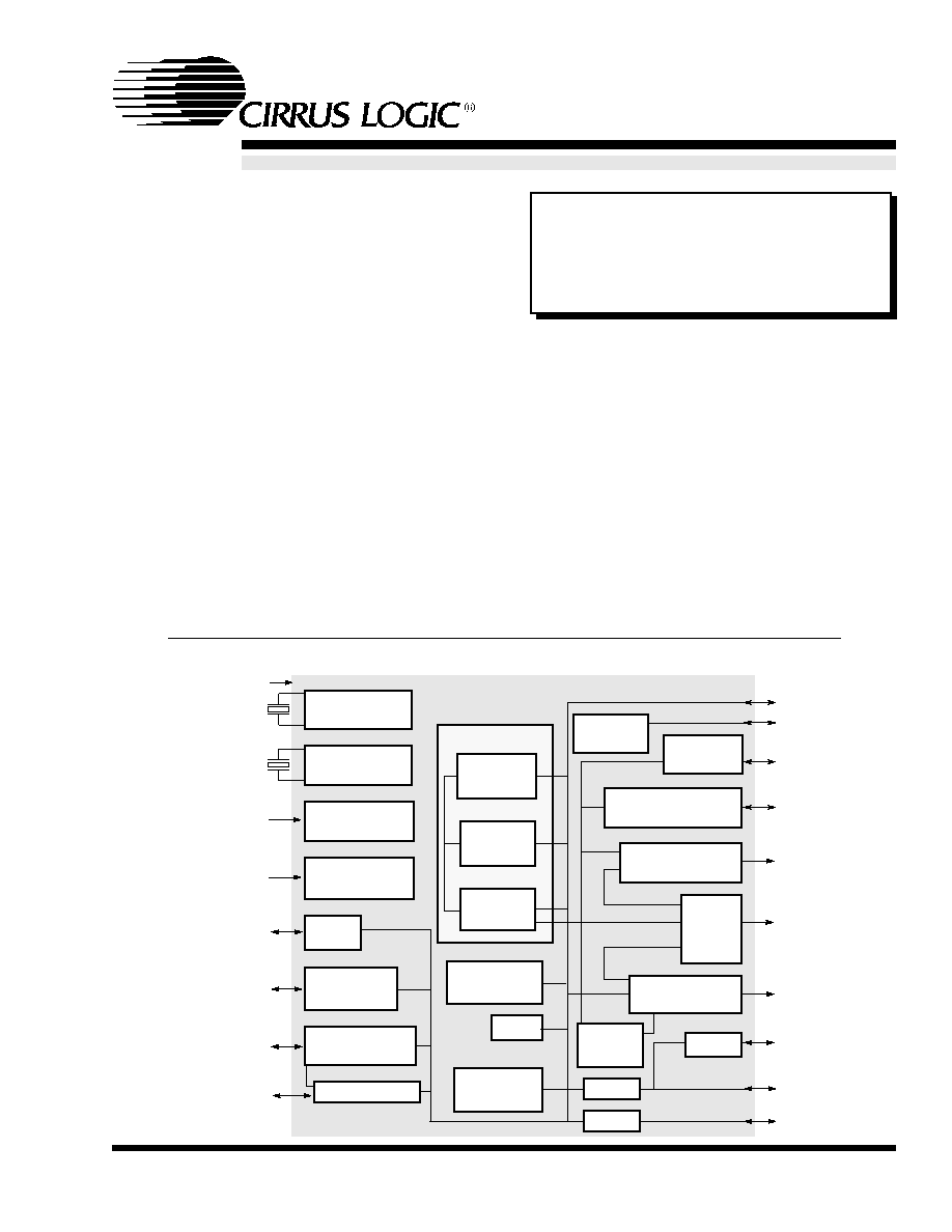
Functional Block Diagram
32.768-kHz
OSCILLATOR
18.432-MHz
PLL
INTERRUPT
CONTROLLER
POWER
MANAGEMENT
SYNC. SERIAL
INTERFACE
STATE
CONTROL
DRAM
CONTROLLER
LCD
CONTROLLER
ARM7
µ
P CORE
8-KBYTE
CACHE
MMU
COUNTERS
(2)
RTC
CODEC INTFC.
ARM710a
INTERNAL DATA BUS
PSU
CONTROL
3.6864 MHz
32.768 kHz
EINT[1≠3], FIQ,
MEDCHG
BATOK, EXTPWR
PWRFL, BATCHG
PORTS A, B, D (8-BIT)
PORT E (3-BIT)
KEYBOARD COLUMN
DRIVERS (0≠7)
BUZZER DRIVE
DC TO DC
ADCCLK, ADCIN,
ADCOUT, SMPCLK,
RXFS, TXFS
PCMCLK, PCMSYNC
PCMIN, PCMOUT
UART
MUX
IRDA
D0≠D31
POR, RUN,
RESET, WAKEUP
EXPCLK, WORD,
CD[0≠3], EXPRDY,
WRITE
MOE, MWE
RAS[0≠1], CAS[0≠3]
A[0≠27],
DRA[0≠12]
LCD DRIVE
LED AND
PHOTODIODE
ASYNC INTERFACE 2
INTERNAL
GPIO
ADDRESS BUS
13-MHz INPUT
ON-CHIP
BOOT ROM
ASYNC INTERFACE 1
SRAM
2 KBYTE
CL-PS6700
INTFC.
PB[0≠1], CS[4≠5]
ROM/EXPANSION
CONTROL
UART

PRELIMINARY DATA BOOK v2.0
September 1997
2
OVERVIEW
CL-PS7111
Low-Power System-on-a-Chip
OVERVIEW
(cont.)
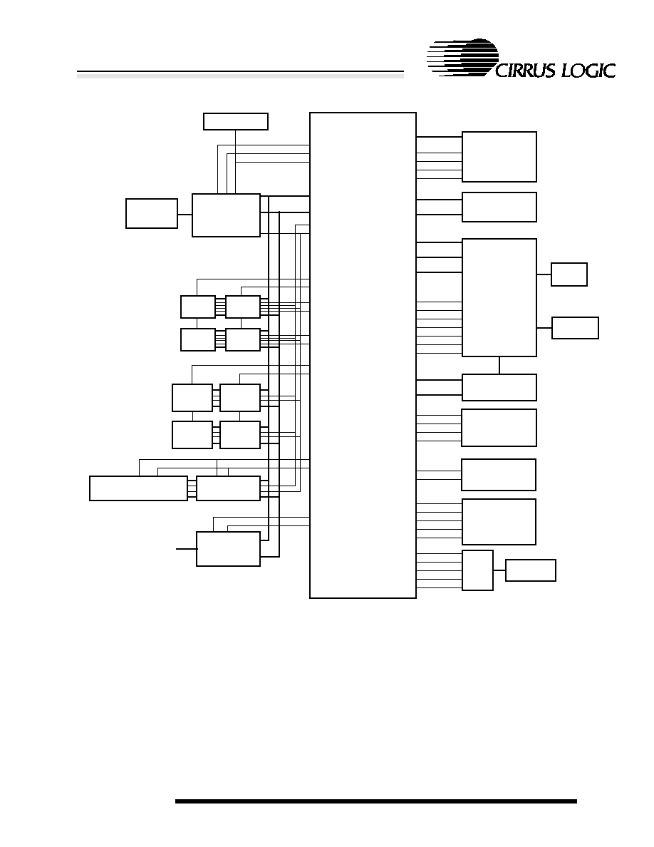
As shown in the system block diagram, simply add-
ing desired memory and peripherals to the highly
integrated CL-PS7111 completes a hand-held
organizer/PDA system board. All the interface logic
is integrated on-chip.
Memory Interface
There are two main external memory interfaces and
a DMA controller that fetches video display data for
the LCD controller from main DRAM memory.
The SRAM/ROM-style interface has programmable
wait-state timings and includes burst-mode capabil-
ity, with six chip selects decoding six 256-Mbyte
sections of addressable space. For maximum flexi-
bility, each bank can be specified to be 8, 16 or 32
bits wide to enable the use of low-cost memory in a
32-bit system. The system can have an 8-bit-wide
boot option to optimize memory size.
The programmable 16- or 32-bit-wide DRAM inter-
face allows direct connection of up to two banks of
DRAM, each bank containing up to 256 Mbytes. To
assure the lowest possible power consumption, the
CL-PS7111 supports self-refresh DRAMs, which
are placed in a low-power state by the device when
it enters low-power standby mode.
Serial Interface
For RS-232 serial communications, the CL-PS7111
includes two UARTs, both of which have two 16-
byte FIFOs for receive and transmit data. The
UARTs support bit rates of up to 115.2 kbps. An
IrDA SIR protocol encoder/decoder can be option-
ally switched into the Rx/Tx signals to/from one of
the UARTs to enable these signals to drive an infra-
red communication interface directly.
A full-duplex codec interface allows direct connec-
tion of a standard codec chip to the CL-PS7111,
allowing storage and playback of sound. A separate
synchronous serial interface supports two industry-
standard protocols (SPI
Æ
and Microwire
Æ
) for inter-
facing to standard devices such as an ADC, allow-
ing for peripheral expansion such as the use of a
digitizer pen.
FEATURES
(cont.)
Mbytes
-- Each segment can be configured as 8, 16, or 32 bits
wide and support page-mode access
-- Programmable access time for conventional
SRAM/ROM/flash memory
s
Support for up to two ultra-low-power CL-PS6700
PC Card controllers
s
2 Kbytes of on-chip SRAM for fast program
execution
s
On-chip boot ROM
s
Two synchronous serial interfaces
-- Supports SPI
Æ
1
or Microwire
Æ
2
-compatible
-- Audio codec
s
27-bit general-purpose I/O
-- Three 8-bit and one 3-bit GPIO port
-- Supports scanning keyboard matrix
1
SPI is a registered trademark of Motorola
Æ
.
2
Microwire is a registered trademark of National
Semiconductor
Æ
.
s
Two UARTs
-- Supports bit rates up to 115.2 kbps
-- Contains two 16-byte FIFOs for Tx and Rx
-- Supports modem control signals
s
SIR (slow -- up to 115.2 kbps -- infrared) encoder
-- IrDA (Infrared Data Association) SIR protocol encoder
can be optionally switched into Tx and Rx signals of
UART 1 up to 115 kbps
s
DC-to-DC converter interface
-- Provides two 96-kHz clock outputs with programmable
duty ratio (from 1-in-16 to 15-in-16)
s
LCD controller
-- Interfaces directly to a single-scan panel monochrome
LCD
-- Panel size is programmable from 16 to 1024 pixels in 16-
pixel increments
-- Video frame size programmable up to 128 Kbytes
-- Bits per pixel programmable from 1, 2, or 4
s
Timer and counters
s
3.3 V at 18.432 MHz and 2.7 V at 13 MHz
s
208-pin VQFP package
s
Evaluation kit available with BOM, schematics,
and design database
September 1997
3
PRELIMINARY DATA BOOK v2.0
OVERVIEW
CL-PS7111
Low-Power System-on-a-Chip
A CL-PS7111≠Based System
LCD MODULE
KEYBOARD
BATTERY
DC-TO-DC
CONVERTERS
ADC
DIGITIZER
IR LED AND
PHOTODIODE
2
◊
RS-232
TRANSEIVER
ADDITIONAL I/O
CL-PS6700 PC
CARD
CONTROLLER
PC CARD
SOCKETS
NCS[4]
PB0
EXPCLK
DD[3:0]
CL1
CL2
FRM
M
D[31:0]
A[27:0]
COL[7:0]
PA[7:0]
DC
INPUT
NMOE
WRITE
NRAS[1]
NRAS[0]
NCAS[0]
NCAS[1]
NCAS[2]
NCAS[3]
PB[7:0]
PD[7:0]
PE[2:0]
NPOR
NPWRFL
BATOK
NEXTPWR
NBATCHG
RUN
WAKEUP
NCS[0]
NCS[1]
DRIVE[1:0]
FB[1:0]
CL-PS7111
ADCCLK
NADCCS
ADCOUT
ADCIN
SMPCLK
LEDDRV
PHDIN
RxD1/2
TxD1/2
DSR
CTS
DCD
C S [n ]
WORD
NCS[2]
NCS[3]
◊
16
DRAM
◊
16
DRAM
◊
16
FLASH
◊
16
FLASH
◊
16
ROM
EXTERNAL MEMORY
MAPPED EXPANSION
BUFFERS
BUFFERS AND
LATCHES
◊
16
ROM
◊
16
DRAM
◊
16
DRAM
POWER
SUPPLY UNIT
AND
COMPARATORS
OSCILLATOR
CODEC
PCMSYNC
PCMOUT
PCMCLK
PCMIN
OVERVIEW
(cont.)
Power Management
The CL-PS7111 is designed for low-power opera-
tion. There are three basic power states:
q
Standby --
This state is equivalent to the com-
puter being switched off (no display), and the
main oscillator shut down.
q
Idle --
In this state
,
the device is functioning and
all oscillators are running, but the processor
clock is halted while waiting for an event such as
a key press.
q
Operating --
This state is the same as the idle
state, except that the processor clock is running.
Packaging
The CL-PS7111 is packaged in a 208-pin VQFP
package, with a body size of 28-mm square, a lead
pitch of 0.5 mm and thickness of 1.4 mm.

PRELIMINARY DATA BOOK v2.0
September 1997
4
OVERVIEW
CL-PS7111
Low-Power System-on-a-Chip
Table of Contents
1.
CONVENTIONS ...................................................................................................................... 6
2.
PIN INFORMATION ................................................................................................................ 8
2.1
Pin Diagram ........................................................................................................................................... 8
2.2
Pin Descriptions ..................................................................................................................................... 9
2.2.1
External Signal Functions ......................................................................................................... 9
2.2.2
Numeric Pin Listing ................................................................................................................. 12
3.
FUNCTIONAL DESCRIPTION ............................................................................................. 16
3.1
Main Functional Blocks ........................................................................................................................ 18
3.2
System Maximization ........................................................................................................................... 20
3.3
Endian Functionality............................................................................................................................. 21
3.4
CPU Core............................................................................................................................................. 22
3.5
Counters............................................................................................................................................... 22
3.5.1
Free-Running Mode ................................................................................................................ 23
3.5.2
Prescale Mode ........................................................................................................................ 23
3.6
Realtime Clock ..................................................................................................................................... 23
3.7
State Control ........................................................................................................................................ 23
3.8
Expansion and ROM Interface ............................................................................................................. 25
3.8.1
CL-PS7111 Boot ROM............................................................................................................ 26
3.8.2
CL-PS6700 PCMCIA controller interface ................................................................................ 27
3.9
DRAM Controller .................................................................................................................................. 30
3.10 LCD Controller ..................................................................................................................................... 33
3.11 Two Internal UARTs and SIR Encoder ................................................................................................. 34
3.12 Clocks .................................................................................................................................................. 35
3.13 Interrupt Controller ............................................................................................................................... 37
3.13.1 Interrupt Latencies in Different States..................................................................................... 38
3.14 Resets .................................................................................................................................................. 39
3.15 Two DC-to-DC Converters ................................................................................................................... 40
3.16 Serial Interface ..................................................................................................................................... 40
3.16.1 Codec Interface ....................................................................................................................... 41
3.16.2 ADC Interface -- Master-Mode Only SSI (Synchronous Serial Interface) .............................. 41
4.
MEMORY MAP ..................................................................................................................... 43
5.
REGISTER DESCRIPTIONS................................................................................................ 44
5.1
Port A Data Register -- PADR ............................................................................................................. 47
5.2
Port B Data Register -- PBDR............................................................................................................. 47
5.3
Port D Data Register -- PDDR ............................................................................................................ 47
5.4
Port A Data Direction Register -- PADDR ........................................................................................... 47
5.5
Port B Data Direction Register -- PBDDR........................................................................................... 47
5.6
Port D Data Direction Register -- PDDDR .......................................................................................... 47
5.7
Port E Data Register -- PEDR............................................................................................................. 47
5.8
Port E Data Direction Register -- PEDDR........................................................................................... 47
5.8.1
System Control Register 1 -- SYSCON1 ............................................................................... 48
5.9
System Status Flags Register 1 -- SYSFLG1 ..................................................................................... 50
5.10 Memory Configuration Register 1 -- MEMCFG1................................................................................. 53
5.10.1 Memory Configuration Register 2 -- MEMCFG2.................................................................... 54
5.11 DRAM Refresh Period Register -- DRFPR ......................................................................................... 57
5.12 Interrupt Status Register 1 -- INTSR1................................................................................................. 58
5.13 Interrupt Mask Register 1 -- INTMR1.................................................................................................. 60

September 1997
5
PRELIMINARY DATA BOOK v2.0
OVERVIEW
CL-PS7111
Low-Power System-on-a-Chip
5.14 LCD Control Register -- LCDCON ......................................................................................................60
5.15 Timer Counter 1 Data Register -- TC1D .............................................................................................62
5.16 Timer Counter 2 Data Register -- TC2D .............................................................................................62
5.17 Realtime Clock Data Register -- RTCDR ............................................................................................62
5.18 Realtime Clock Match Register -- RTCMR .........................................................................................62
5.19 Pump Control Register -- PMPCON ...................................................................................................63
5.20 Codec Interface Data Register -- CODR.............................................................................................64
5.21 UART Data Registers -- UARTDR1≠2 ................................................................................................64
5.22 UART Bit Rate and Line Control Registers -- UBRLCR1≠2................................................................65
5.23 Synchronous Serial ADC Interface Data Register --
SYNCIO ............................................................67
5.24 Least-Significant Word-LCD Palette Register -- PALLSW...................................................................68
5.25 Most-Significant Word-LCD Palette Register -- PALMSW...................................................................68
5.26 Clear All Start Up Reason Flags Location -- STFCLR........................................................................69
5.27 Battery Low End-of-Interrupt -- BLEOI................................................................................................69
5.28 Media Changed End-of-Interrupt -- MCEOI ........................................................................................69
5.29 Tick End-of-Interrupt Location -- TEOI ................................................................................................69
5.30 End--of-Interrupt Location -- TC1EOI TC1 ..........................................................................................69
5.31 End-of-Interrupt Location -- TC2EOI TC2 ...........................................................................................69
5.32 RTC Match End-of-Interrupt -- RTCEOI..............................................................................................69
5.33 UART1 Modem Status Changed End-of-Interrupt -- UMSEOI............................................................69
5.34 Codec End-of-Interrupt Location -- COEOI.........................................................................................69
5.35 Enter Idle State Location -- HALT .......................................................................................................69
5.36 Enter Standby State Location -- STDBY.............................................................................................69
5.37 LCD Frame Buffer Start Address -- FRBADDR ..................................................................................70
5.38 System Control Register 2 -- SYSCON2 ............................................................................................70
5.39 System Status Flags Register 2 -- SYSFLG2 .....................................................................................71
5.40 Interrupt Status Register 2 -- INTSR2.................................................................................................72
5.41 Interrupt Mask Register 2 -- INTMR2..................................................................................................72
5.42 Keyboard End-of-Interrupt Location -- KBDEOI ..................................................................................72
6.
ELECTRICAL SPECIFICATIONS .........................................................................................73
6.1
Absolute Maximum Ratings .................................................................................................................73
6.2
Recommended Operating Conditions ..................................................................................................73
6.3
DC Characteristics ...............................................................................................................................74
6.4
AC Characteristics ...............................................................................................................................75
6.5
I/O Buffer Characteristics .....................................................................................................................87
6.6
Test Modes...........................................................................................................................................87
6.6.1
Oscillator and PLL Bypass Mode ............................................................................................88
6.6.2
Functional (EPB) Test Mode....................................................................................................88
6.6.3
Oscillator and PLL Test Mode .................................................................................................88
6.6.4
Pin Test Mode..........................................................................................................................89
6.6.5
High-Z (System) Test Mode.....................................................................................................89
6.6.6
Software-Selectable Test Functionality....................................................................................90
7.
PACKAGE SPECIFICATIONS...............................................................................................91
7.1
208-Pin VQFP Package Outline Drawing .............................................................................................91
8.
ORDERING INFORMATION .................................................................................................92
A.
BOOT CODE..........................................................................................................................93
BIT INDEX..............................................................................................................................99
INDEX ..................................................................................................................................101