 | –≠–ª–µ–∫—Ç—Ä–æ–Ω–Ω—ã–π –∫–æ–º–ø–æ–Ω–µ–Ω—Ç: CPC1335P | –°–∫–∞—á–∞—Ç—å:  PDF PDF  ZIP ZIP |
Part #
Description
CPC1335P
8 Pin Flatpack (50/Tube)
CPC1335PTR
8 Pin Flatpack (1000/Reel)
CPC1335P
Units
Blocking Voltage
350
V
Load Current
100
mA
Max R
ON
35
LED Current to Operate
1.0
mA
www.clare.com
DS-CPC1335P-R2.0
CPC1335P
Single Pole OptoMOS
Æ
Relay with
Bi-directional Transient Protection
1
Applications
Features
Description
Approvals
Ordering Information
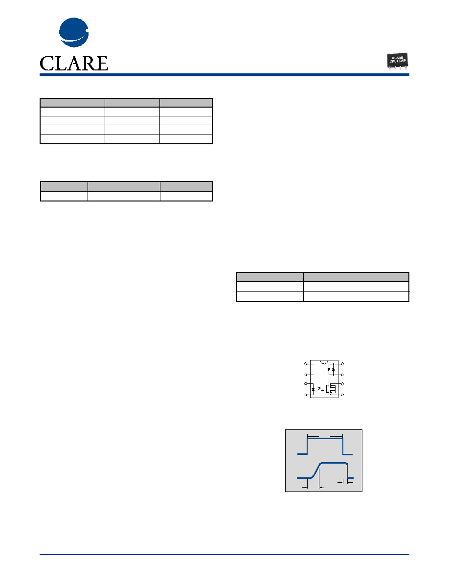
Pin Configuration
Switching Characteristics of
Normally Open (Form A) Devices
CONTROL
LOAD
10ms
10%
10%
90%
+
T
ON
T
OFF
+
+
∑
Security
∑
Aerospace
∑
Industrial Controls
∑
Small 8 Pin Surface Mount Package
∑
Low Drive Power Requirements (TTL/CMOS
Compatible)
∑
No Moving Parts
∑
High Reliability
∑
Arc-Free With No Snubbing Circuits
∑
3750V
RMS
Input/Output Isolation
∑
No EMI/RFI Generation
∑
Machine Insertable, Wave Solderable
∑
Tape & Reel Version Available
CPC1335P is a 1 Form-A solid state relay with
Bi-directional TVS relay protection. The efficient
MOSFET switches and photovoltaic die that use Clare's
patented OptoMOS
Æ
architecture to provide 3750 V
RMS
of input to output isolation. The optically coupled input
is controlled by highly efficient GaAIAs infrared LEDs.
The device is available in an 8 pin space saving sur-
face mount package. The transient voltage suppressor
is designed to meet the requirements of EN50130-4
(installation class 3).
∑
UL pending.
1
2
3
4
8
7
6
5
+ Control - Switch
– Control - Switch
TVS +/-
TVS +/-
Load - Switch
Load - Switch
CPC1335P Pinout
Relay Characteristics
Part Number
Peak Pulse Power
V
WM
CPC1335P
600W
40.2V
Transient Protection Characteristics
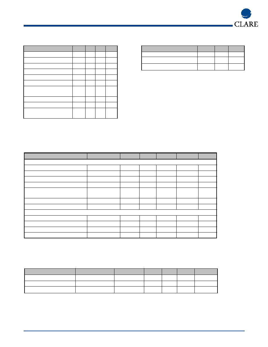
Parameter
Conditions
Symbol
Min
Typ
Max
Units
Output Characteristics @ 25∞C
Load Current (Continuous) AC Peak
1
I
F
=2mA
I
L
-
-
100
mA
Peak Load Current
10ms max
I
LPK
-
-
350
mA
On-Resistance
2
I
L
=100mA R
ON
-
25
35
Off-State Leakage Current
V
L
=350V
I
LEAK
-
-
1
µA
Switching Speeds
Turn-On
I
F
=2mA, V
L
=10V
T
ON
-
-
10
ms
Turn-Off
I
F
=2mA, V
L
=10V
T
OFF
-
-
10
ms
Output Capacitance
50V
RMS
; f=1MHz
C
OUT
-
25
-
pF
Input Characteristics @ 25∞C
Input Control Current
3
I
L
=100mA
I
F
1
-
50
mA
Input Voltage Drop
I
F
=5mA
V
F
0.9
1.2
1.4
V
Reverse Input Current
V
R
=5V
I
R
-
-
10
µA
Input to Output Capacitance
-
C
I/O
-
3
-
pF
1
Load current derates linearly from 100 mA @ 25∞C to 70ma @ 85∞C
2
Measurement taken within 1 second of on time
3
For applications requiring high temp operation (greater than 60∞C) a minimum LED drive current of 3mA is recommended.
Electrical Characteristics: Relay
Electrical Characteristics: TVS
Parameter
Min
Typ Max Units
Input Power Dissipation
-
-
150
1
mW
Input Control Current
-
-
50
mA
Peak (10ms)
-
-
1
A
Reverse Input Voltage
-
-
5
V
Total Power Dissipation
-
-
800
2
mW
Blocking Voltage
-
-
350
V
Isolation Voltage
Input to Output
3750
-
-
V
RMS
Operational Temperature
-40
-
+85
∞C
Storage Temperature
-40
-
+125
∞C
Soldering Temperature
(10 Seconds Max.)
-
-
+220
∞C
1
Derate Linearly 1.33 mw/∞C
2
Derate Linearly 6.67 mw/∞C
www.clare.com
2
CPC1335P
Rev. 2.0
Absolute Maximum Ratings are stress ratings. Stresses in
excess of these ratings can cause permanent damage to
the device. Functional operation of the device at these or
any other conditions beyond those indicated in the opera-
tional sections of this data sheet is not implied. Exposure
of the device to the absolute maximum ratings for an
extended period may degrade the device and effect its
reliability.
Absolute Maximum Ratings - Relay (@ 25∞ C)
Absolute Maximum Ratings
Symbol
Max
Units
Peak Pulse Power
(Ipp=9.3A, 10/1000µs pulse)
P
PP
600
W
Max Stand-Off/Working Voltage
V
WM
40.2
V
Absolute Maximum Ratings
Parameter
Conditions
Symbol
Min
Typ
Max
Units
Clamping Voltage
(Ipp=9.3A)
V
C
-
-
64.8
V
Reverse Breakdown Voltage
(I
BR
=1000 µA)
V
BR
44.4
-
-
V
Reverse Leakage Current
(V
WM
=40.2 V)
I
D
- -
5
µA

CPC1335P
www.clare.com
3
Rev. 2.0
*The Performance data shown in the graphs above is typical of device performance. For guaranteed parameters not indicated in the written specifications, please contact our application
department.
PERFORMANCE DATA*
CPC1335P
Typical LED Forward Voltage Drop
(Ambient Temperature = 25 C)
I
F
= 5mADC
35
30
25
20
15
10
5
0
1.17
1.19
1.21
1.23
1.25
LED Forward Voltage Drop (V)
Device Count (N)
o
CPC1335P
Typical On-Resistance Distribution
(Ambient Temperature = 25 C)
(Load Current = 120mA)
35
30
25
20
15
10
5
0
26
28
30
32
27
29
31
On-Resistance (
)
Device Count (N)
o
CPC1335P
Typical Blocking Voltage Distribution
(Ambient Temperature = 25 C)
35
30
25
20
15
10
5
0
377.5
399.5
421.5
443.5
388.5
410.5
432.5
Blocking Voltage (V)
Device Count (N)
o
CPC1335P
Typical I
F
for Switch Operation
(Ambient Temperature = 25 C)
(Load Current = 100mA)
0.35
0.45
0.55
0.30
0.40
0.50
0.60
LED Current (mA)
Device Count (N)
25
20
15
10
5
0
o
CPC1335P
Typical Turn-On Time
(Ambient Temperature = 25 C)
(Load Current = 100mA; I
F
= 5mA)
0.50
0.70
0.90
1.10
0.60
0.80
1.00
Turn-On (ms)
Device Count (N)
25
20
15
10
5
0
o
CPC1335P
Typical Turn-Off Time
(Ambient Temperature = 25 C)
(Load Current = 100mA; I
F
= 5mA)
0.26
0.30
0.34
0.38
0.36
0.32
0.28
Turn-Off (ms)
Device Count (N)
25
20
15
10
5
0
o
CPC1335P
Typical Load Current vs. Temperature
Temperature ( C)
Load Current (mA)
180
160
140
120
100
80
60
40
20
0
-40 -20
0
20
40
60
80
120
100
I =2mA
F
I =5mA
F
o
CPC1335P
Typical Leakage vs. Temperature
(Measured across Pins 5 & 6) I
L
= max rated
Temperature ( C)
Leakage (
µ
A)
-40
0.016
0.014
0.012
0.010
0.008
0.006
0.004
0.002
0
-20
0
20
40
60
80
100
o
CPC1335P
Typical Blocking Voltage
vs. Temperature
Temperature ( C)
Blocking Voltage (V
RMS
)
-40
430
425
420
415
410
405
400
395
-20
0
20
40
60
80
100
o
CPC1335P
Typical Turn-Off vs. Temperature
(Load Current = 50mA)
Temperature ( C)
Turn-Off (ms)
-40
1.000
0.900
0.800
0.700
0.600
0.500
0.400
0.300
0.200
0.100
0
-20
0
20
40
60
80
100
o
I =5mA
F
I =2mA
F
CPC1335P
Typical LED Forward Voltage Drop
vs. Temperature
Temperature ( C)
LED Forward Voltage Drop (V)
1.8
1.6
1.4
1.2
1.0
0.8
-40
-20
0
20
40
60
80
120
100
50mA
10mA
5mA
o
CPC1335P
Typical Turn-Off vs. LED Forward Current
(Load Current = 100mA)
LED Forward Current (mA)
Turn-Off (ms)
0
5
10
15
20
25
30
35
40
45
0.7
0.6
0.5
0.4
0.3
0.2
0.1
0
50
www.clare.com
4
CPC1335P
Rev. 2.0
*The Performance data shown in the graphs above is typical of device performance. For guaranteed parameters not indicated in the written specifications, please contact our application
department.
PERFORMANCE DATA*
CPC1335P
Typical On-Resistance vs. Temperature
(Load Current = 50mA; I
F
= 3mA)
Temperature ( C)
On-Resistance ( )
-40
60
50
40
30
20
10
0
-20
0
20
40
60
80
100
o
CPC1335P
Typical Load Current vs. Load Voltage
(Ambient Temperature = 25 C)
I
F
= 5mA
Load Voltage (V)
Load Current (mA)
150
100
50
0
-50
-100
-150
-3
-2
-1
0
1
2
3
o
CPC1335P
Energy Rating Curve
Time
Load Current (A)
10µs
1.0
0.9
0.8
0.7
0.6
0.5
0.4
0.3
0.2
0.1
0
1ms
100µs
100ms 1s
10ms
10s 100s
CPC1335P
www.clare.com
5
Rev. 2.0
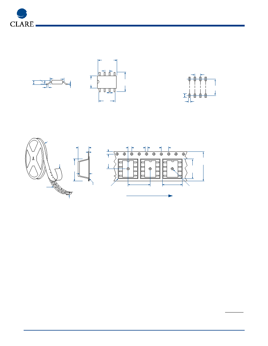
Dimensions
mm
(inches)
MECHANICAL DIMENSIONS
PC Board Pattern
(Top View)
2.540
± .127
(.100
± .005)
8.763
± .127
(.345
± .005)
1.193
(.047)
.787
(.031)
8 Pin Flatpack ("P" Suffix)
7.620
± .254
(.300
± .010)
2.159 TYP.
(.085)
2.286 MAX.
(.090)
9.398
± .127
(.370
± .005)
6.350
± .127
(.250
± .005)
9.652
± .381
(.380
± .015)
2.540
± .127
(.100
± .005)
8.077
± .127
(.318
± .005)
.457
± .076
(.018
± .003)
.203
(.008)
.635
± .127
(.025)
Tape and Reel Packaging for 8 Pin Flatpack Package
7.493
± .102
(.295
± .004)
12.090
(.476)
1.753
± 0.102
(.069
± .004)
3.987
± .102
(.157
± .004)
1.498
± .102
(.059
± .004)
6.731 MAX.
(.265)
.406 MAX.
(.016)
4.877
(.192)
Top Cover
Tape
2.007
± .102
(.079
± .004)
11.988
± .102
(.472
± .004)
User Direction of Feed
.050R TYP.
16.002
± .305
(.630
± .012)
10.287
(.405)
Embossment
Embossed Carrier
Top Cover
Tape Thickness
.102 MAX.
(.004)
10.287
± .102
(.405
± .004)
1.549
± .102
(.061
± .004)
330.2 DIA.
(13.00)
1
8

Clare, Inc. makes no representations or warranties with respect to the accuracy or completeness of the contents of this publication and reserves the right to make changes to specifications and product descriptions
at any time without notice. Neither circuit patent licenses nor indemnity are expressed or implied. Except as set forth in Clare's Standard Terms and Conditions of Sale, Clare, Inc. assumes no liability whatsoever, and
disclaims any express or implied warranty, relating to its products including, but not limited to, the implied warranty of merchantability, fitness for a particular purpose, or infringement of any intellectual property right.
The products described in this document are not designed, intended, authorized or warranted for use as components in systems intended for surgical implant into the body, or in other applications intended to sup-
port or sustain life, or where malfunction of Clare's product may result in direct physical harm, injury, or death to a person or severe property or environmental damage. Clare, Inc. reserves the right to discontinue or
make changes to its products at any time without notice.
For additional information please visit our website at: www.clare.com
Specification: DS-CPC1335P-R2.0
©Copyright 2002, Clare, Inc.
OptoMOS
Æ
is a registered trademark of Clare, Inc.
All rights reserved. Printed in USA.
11/19/02