
Voltage: 2.4 - 39 Volts
Power: 410 mWatts
CZR
W55C2V4 Thru 55C39
Features
Planar Die construction
410mW Power Dissipation
Zener Voltages from 2.4V - 39V
Ideally Suited for Automated Assembly
Processes
Mechanical data
Case: SOD-123, MoldedPlastic
Terminals: Solderable per MIL-STD-202,
Method 208
Approx. Weight: 0.008 gram
Surface Mount Zener Diodes
www.comchip.com.tw
COMCHIP
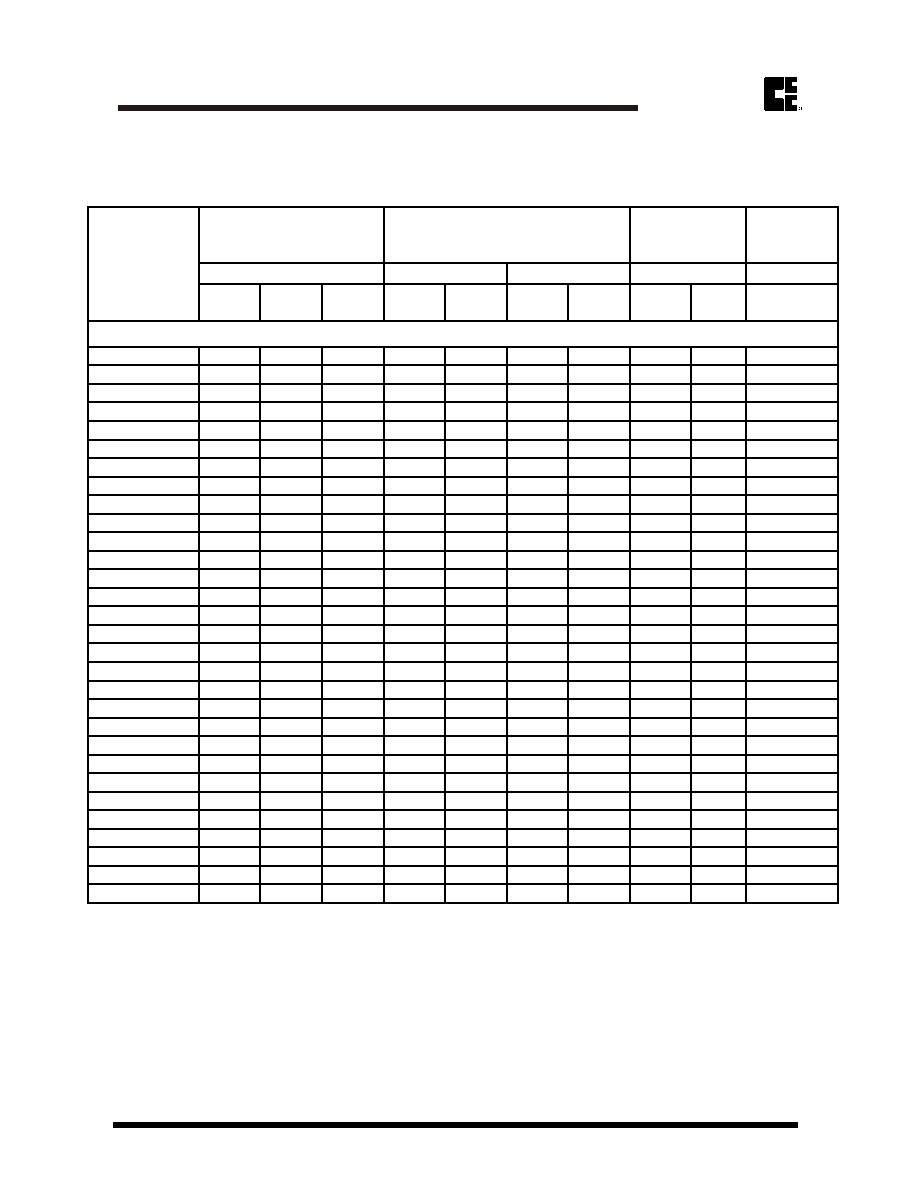
Maximum Ratings and Electrical Characterics
Parameter
Symbol
Value
Units
Power Dissipation (Note A) at 25∞C
P
D
410
mW
Peak Forward Surge Current Surge, 8.3ms Single
Half Sine-wave Superimposed on Rated Load
(JEDEC Method) (Note B)
I
FSM
2.0
Amps
Operating Junction and Storage Temperature Range
T
J
-55 to +150
∞C
Dimensions in inches and (millimeters)
SOD-123
MDS0302005A
Page 1
.154 (3.90)
.016 (.40)Min.
.005 (.12) MAX.
.098 (2.50)
.110 (2.80)
.141 (3.60)
.
037(0.95)
.
053(1.35)
.
008(0.20)
Max.
.
055(1.40)
.
071(1.80)
.
019(0.50)
.
028(0.70)
NOTES:
A. Mounted on 5.0mm
2
(.013mm thick) land areas.
B. Measured on 8.3ms, single half sine-wave or equivalent square wave, duty cycle = 4 pulses per minute maximum.
MDS0302005A
Page 2
Surface Mount Zener Diodes
www.comchip.com.tw
COMCHIP
I
ZM
@ T
A
Nom. V Min. V Max. V
Ohm
mA
Ohm
mA
nA
V
mA
CZRW55C2V4
2.4
2.28
2.56
85
5
600
1
100000
1
-
CZRW55C2V7
2.7
2.5
2.9
83
5
500
1
75000
1
134
CZRW55C3V0
3.0
2.8
3.2
95
5
500
1
50000
1
118
CZRW55C3V3
3.3
3.1
3.5
95
5
500
1
25000
1
109
CZRW55C3V6
3.6
3.4
3.8
95
5
500
1
15000
1
100
CZRW55C3V9
3.9
3.7
4.1
95
5
500
1
10000
1
92
CZRW55C4V3
4.3
4
4.6
95
5
500
1
5000
1
84
CZRW55C4V7
4.7
4.4
5
78
5
500
1
5000
1
76
CZRW55C5V1
5.1
4.8
5.4
60
5
480
1
100
0.8
67
CZRW55C5V6
5.6
5.2
6
40
5
400
1
100
1
59
CZRW55C6V2
6.2
5.8
6.6
10
5
200
1
100
2
54
CZRW55C6V8
6.8
6.4
7.2
8
5
150
1
100
3
49
CZRW55C7V5
7.5
7
7.9
7
5
50
1
100
5
44
CZRW55C8V2
8.2
7.7
8.7
7
5
50
1
100
6
40
CZRW55C9V1
9.1
8.5
9.6
10
5
50
1
100
7
36
CZRW55C10
10.0
9.4
10.6
15
5
70
1
100
7.5
33
CZRW55C11
11.0
10.4
11.6
20
5
70
1
100
8.5
30
CZRW55C12
12.0
11.4
12.7
20
5
90
1
100
9
28
CZRW55C13
13.0
12.4
14.1
25
5
110
1
100
10
25
CZRW55C15
15
13.8
15.6
30
5
110
1
100
11
23
CZRW55C16
16
15.3
17.1
40
5
170
1
100
12
20
CZRW55C18
18
16.8
19.1
50
5
170
1
100
14
18
CZRW55C20
20
18.8
21.2
50
5
220
1
100
15
17
CZRW55C22
22
20.8
23.3
55
5
220
1
100
17
16
CZRW55C24
24
22.8
25.6
80
5
220
1
100
18
13
CZRW55C27
27
25.1
28.9
80
5
250
1
100
20
12
CZRW55C30
30
28
32
80
5
250
1
100
22.5
10
CZRW55C33
33
31
35
80
5
250
1
100
25
9
CZRW55C36
36
34
38
90
5
250
1
100
27
9
CZRW55C39
39
37
41
90
5
300
1
100
29
8
I
R
@ V
R
Max Reverse
Leakage
Current
Max Zener
Current
NOTE:
1.Tolerance and Type Number Designation. The type numbers listed have a standard tolerance on the nominal zener voltage of ±5%.
2.Specials Available Include:
A. Nominal zener voltages between the voltages shown and tighter voltage tolerances.
B. Matched sets.
3.Zener Voltage (VZ) Measurement. Guarantees the zener voltage when measured at 90 seconds while maintaining the lead temperature (TL) at 30OC, from the diode body.
4.Zener Impedance (ZZ) Derivation. The zener impedance is derived from the 60 cycle ac voltage, which results when an AC current having an rms value equal to 10% of the dc zener
current (IZT or IZK) is superimposed on IZT or IZK.
5.Surge Current (IR) Non-Repetitive. The rating listed in the electrical characteristics table is maximum peak, non-repetitive, reverse surge current of 1/2 square wave or equivalent sine
wave pulse of 1/120 second duration superimposed on the test current, IZT, per JEDEC registration; however, actual device capability is as described in Figure 5.
Maximum Ratings and Electrical Characterics
(TA=25∞C unless otherwise noted) V
F
=1.2V max, I
F
=100mA for all types
Max. Zener Impedance
Nominal Zener Voltage
410 mWatts Zener Diodes
V
Z
@ I
ZT
Z
ZT
@ I
ZT
Z
ZK
@ I
ZK
Part Number

Rating and Characteristic Curves (CZRW55C2V4 Thru CZRW55C39)
MDS0302005A Page 3
Surface Mount Zener Diodes
www.comchip.com.tw
COMCHIP
TYPICAL REVERSE CURRENT
TEMPERA
TURE
COEFFICIENT
,mV
/
C
)
o
NOMINAL ZENER VOLTAGE, Volts
-1
0
1
2
3
4
5
6
7
8
12
11
10
9
8
7
6
5
4
3
2
-2
-3
100
10
1
1000
100
10
1
IZ = 1 mA
5 mA
20 mA
DYNAMIC
IMPEDANCE,
W
NORMAL ZENER VOLTAGE, Volts
T
J
=25 C
O
I
Z(AC)=0.1
I
F=1 kHZ
Z(DC)
FOR
W
ARD
CURRENT
,m
A
TYPICAL FORWARD VOLTAGE
FORWARD VOLTAGE, Volts
1.2
1.1
1.0
0.9
0.8
0.7
0.6
0.5
0.4
1000
100
10
1
75 C
O
5 C
O
25 C
O
150 C
O
100
1000
100
10
1
10
1
BIAS AT
50% OF VZ NOM
0 V BIAS
1 V BIAS
CAP
ACIT
ANCE,
pF
NOMINAL ZENER VOLTAGE, Volts
T =25 C
A
o
100
10
1
NOMINAL ZENER VOLTAGE, Volts
TEMPERA
TURE
COEFFICIENT
,mV
/
C
)
o
10
100
TEMPERATURE ( C)
o
POWER
DISSIP
A
TION,
W
atts
1.2
1.0
0.8
0.6
0.4
0.2
0
150
125
100
75
50
25
P
D V
.
S
. T
A
155

MDS0302005A Page 4
Surface Mount Zener Diodes
www.comchip.com.tw
COMCHIP
90
1000
100
10
1
0.1
0.01
0.001
0.0001
0.00001
80
70
60
50
40
30
20
10
0
LEAKAGE
CURRENT
(
A)
m
NOMINAL ZENER VOLTAGE, Vlots
+150 C
O
+25 C
O
-55 C
O
12
100
10
1
0.1
0.01
10
8
6
4
2
0
ZENER
CURRENT
,m
A
ZENER VOLTAGE, Volts
T =25 C
A
o
100
10
1
0.1
0.01
10
30
50
70
90
T =25 C
A
o
ZENER VOLTAGE, Volts
ZENER VOLTAGE V.S. ZENER CURRENT
ZENER
CURRENT
,m
A
Rating and Characteristic Curves (CZRW55C2V4 Thru CZRW55C39)