CYNTEC CO., LTD.
DOCUMENT : TBF2520245A1
REVISION : A0
PAGE : 1 OF 7
TBF-2520-245-A1 SERIES THIN FILM BAND PASS FILTER
1. Feature:
1. 2.45GHz Thin Film Band Pass Filter
2. For ISM Band applications like Wireless LAN & Bluetooth.
3. Lead Free
2. Part Number
TBF -- 2520 -- 245 --A1
--
XX
(1) (2) (3)
(4) (5)
Where
(1) TBF : Thin Film Band Pass Filter
(2)
Size
:
4 digits of number ≠≠2520 = 2.50◊2.00 mm
(3) Center Frequency :
245 = 2.45 GHz
(4)
Type
Refer to Table 3-1
(5)
XX
Internal Code
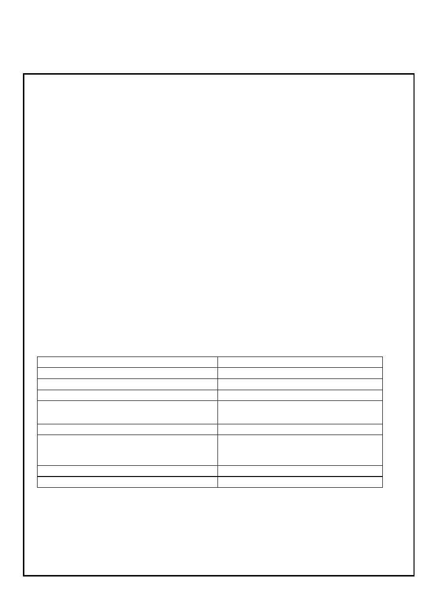
3. Ratings
3-1 Specifications
Part Number
TBF-2520-245-A1
Nominal Characteristics Impedance
50
Nominal Center Frequency
2450MHz
Bandwidth
2400 ~ 2500MHz
Insertion Loss
1.7 dB Max. at +25
1.9 dB max. at ≠40 ~ +85
Ripple in BW
0.5dB max.
Attenuation
25.0dB min. at 1750MHz
25.0dB min. at 2000 ~ 2100MHz
22.0dB min at 4800 ~ 5000MHz
VSWR in BW
2.0 Max.
Power Capacity
500mW Max.
3-2 Operation Temperature:
-40 to +85
3-3 Storage Temperature: +15 to +35

CYNTEC CO., LTD.
DOCUMENT : TBF2520245A1
REVISION : A0
PAGE : 2 OF 7
4. Outline Dimension
5. Electrical Performance
Code
Dimension Code Dimension
L 2.5
± 0.2
L1
2.0
± 0.1
W 2.0
± 0.2
Lt
1.2
± 0.1
T 0.5
± 0.1
Lw
0.2
± 0.1
W1
0.8
± 0.1
Wt
0.4
± 0.1
Ww
0.2
± 0.1
Unit : mm
Terminal Configuration:
Terminal No.
Terminal Name
(1) GND
(2) Output
(3) GND
(4) Input

CYNTEC CO., LTD.
DOCUMENT : TBF2520245A1
REVISION : A0
PAGE : 3 OF 7
6. Recommended Land Pattern
Line Width be designed to match 50ohm characteristic impedance, depending on PCB material
and thickness
Notes : All the technical data and information contained herein are subject to change without prior
notice

CYNTEC CO., LTD.
DOCUMENT : TBF2520245A1
REVISION : A0
PAGE : 4 OF 7
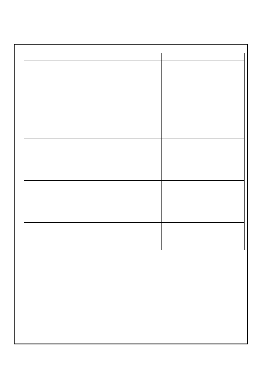
7. Reliability Test
7-1 Electrical
ITEM
Specification and Requirement
Test Method
Temperature
Characteristics
Satisfy electrical characteristics
Solder the sample on PCB.
Exposure at each temperature,
-40, -20, 0, +25, +50,
+85 for 30minutes
7-2 Mechanical
ITEM
Specification and Requirement
Test Method
Solderability
The Surface of terminal immersed shall
be minimum of 95% covered with a
new coating of solder
Solder bath :
After immersing in flux, dip in
245
± 5 molten solder bath
for 2
± 0.5 seconds
Resistance to solder
Heat
Satisfy electrical characteristics without
distinct deformation in appearance
(1) Pre-heat : 100 ~ 110 for
30 seconds
(2) Immersed at solder bath of
270
± 5 for 20 ± 1 seconds
Vibration
Satisfy electrical characteristics without
Mechanical damage such as break
Vibrate as apply 20 to 2,000Hz,
186m/s
2
(19G) acceleration 1.5mm
amplitude for 2 hours in each of three
(X, Y, Z) axis (total 6 hours).
Shock
Satisfy electrical characteristics without
mechanical damaged such as break
(1) Break value : 490 N
(2) Duration of pulse : 11ms
(3) 3 times in each positive and
negative direction of 3 mutual
perpendicular directions.
Bending Test
Satisfy electrical characteristics without
mechanical damage such as break
Bending value : 3mm for
30
± 1 seconds
Solvent Resistant
Marking should be legible without
mechanical and distinct damage in
appearance
(1)
Solvent : Trichloroethane or
Isopropyl alcohol.
(2) Immersed in solvent at room
temperature for 90 seconds
Drop Test
Satisfy electrical characteristics without
mechanical damage
Drop the sample from a height of 1m
to concrete ground for 10 times
CYNTEC CO., LTD.
DOCUMENT : TBF2520245A1
REVISION : A0
PAGE : 5 OF 7
7-3 Load Life
ITEM
Specification and Requirement
Test Method
Rapid change of
temperature
Satisfy Electrical Characteristics.
Without distinct damage.
Perform 5 cycles as follows :
-55 for 30minutes room
temperature for 3 minutes
+125 for 30minutes room
temperature for 3 minutes.
(Dwell time : 5 to 8 minutes)
Humidity Resistance
Test
Satisfy Electrical Characteristics.
Without distinct damage.
Precondition at +25 for 1hour.
Let stand at temperature +40
± 3,
90~95% relative humidity for 1,000
hours before taking final
measurements.
Low Temperature
Store
Satisfy Electrical Characteristics.
Without distinct damage.
Solder the sample on PCB.
Exposure at
-55 ± 3 for 1,000
hours.
1~2 hours exposure at room
temperature and humidity, prior to
measurement.
High Temperature
Store
Satisfy Electrical Characteristics.
Without distinct damage.
Solder the sample on PCB.
Exposure at +85
± 3 for 1,000
hours.
1~2 hours exposure at room
temperature and humidity, prior to
measurement.
Load Life
Satisfy Electrical Characteristics.
Without distinct damage.
Apply 16 Volt voltage at 70
± 2
ambient

CYNTEC CO., LTD.
DOCUMENT : TBF2520245A1
REVISION : A0
PAGE : 6 OF 7
8. Packaging
8-1 Material : Paper Carrier Tape
8-2 Dimensions
8-2-1 Tape packaging dimensions
Direction mark
Carries cavity
A
0.65 ± 0.10
B
A = 2.28 ± 0.10
B = 2.74 ± 0.10
P(PITCH) = 4.00 ± 0.10
+
1.5
-
P
1.75 ± 0.10
8.00 ± 0.30
P
Unit : mm
Sprocket hole
0.60 ± 0.10
2.00 ± 0.10
3.50 ± 0.10
0.1
8-2-2 Setting Direction
8-2-3 Reel dimensions
Unit : mm
10.0 ± 1.5
0.8 ± 0.2
2.0 ± 0.5
21 ± 0.8
13
.0 ± 0.
5
60
±
5.0
1
78 ± 2

CYNTEC CO., LTD.
DOCUMENT : TBF2520245A1
REVISION : A0
PAGE : 7 OF 7
8-3 Peel force of top cover tape
The peel speed shall be about 300 mm/minute
The peel force of top cover tape shall be between 10 to 70g
8-4 Numbers of taping
4,000 pieces/reel
8-5 Label marking
The following items shall be marked on the production and shipping
Label on the reel.
8-5-1 Production Label
(1) Part No.
(2) Description
(3) Quantity
(4) Taping No.
8-5-2 Shipping Label
(1) *Customer's name
(2) *Customer's part No.
(3) Manufacturer's part No.
(4) Manufacturer's name
(5) Manufacturer's country
*Note : Item (1) and (2) are listed by request