 | –≠–ª–µ–∫—Ç—Ä–æ–Ω–Ω—ã–π –∫–æ–º–ø–æ–Ω–µ–Ω—Ç: 27H010 | –°–∫–∞—á–∞—Ç—å:  PDF PDF  ZIP ZIP |
128K x 8 High-Speed CMOS EPROM
fax id: 3023
CY27H010
Cypress Semiconductor Corporation
∑
3901 North First Street
∑
San Jose
∑
CA 95134
∑
408-943-2600
August 1994 ≠ Revised March 1997
1CY 27H0 10
Features
∑ CMOS for optimum speed/power
∑ High speed
-- t
AA
= 25 ns max. (commercial)
-- t
AA
= 35 ns max. (military)
∑ Low power
-- 275 mW max.
-- Less than 85 mW when deselected
∑ Byte-wide memory organization
∑ 100% reprogrammable in thewindowed package
∑ EPROM technology
∑ Capable of withstanding >2001V static discharge
∑ Available in
-- 32-pin PLCC
-- 32-pin TSOP-I
-- 32-pin, 600-mil plastic or hermetic DIP
-- 32-pin hermetic LCC
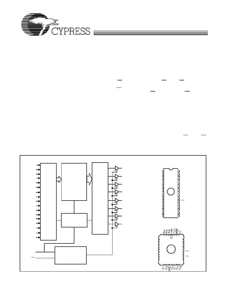
Functional Description
The CY27H010 is a high-performance, 1-megabit CMOS
EPROM organized in 128 Kbytes. It is available in indus-
try-standard 32-pin, 600-mil DIP, LCC, PLCC, and TSOP-I
packages. These devices offer high-density storage com-
bined with 40-MHz performance. The CY27H010 is available
in windowed and opaque packages. Windowed packages al-
low the device to be erased with UV light for 100% re-
programmability.
The CY27H010 is equipped with a power-down chip enable
(CE) input and output enable (OE). When CE is deasserted,
the device powers down to a low-power stand-by mode. The
OE pin three-states the outputs without putting the device into
stand-by mode. While CE offers lower power, OE provides a
more rapid transition to and from three-stated outputs.
The memory cells utilize proven EPROM floating-gate technol-
ogy and byte-wide intelligent programming algorithms. The
EPROM cell requires only 12.75 V for the supervoltage and
low programming current allows for gang programming. The
device allows for each memory location to be tested 100%,
because each location is written to, erased, and repeatedly
exercised prior to encapsulation. Each device is also tested
for AC performance to guarantee that the product will meet DC
and AC specification limits after customer programming.
The CY27H010 is read by asserting both the CE and the OE
inputs. The contents of the memory location selected by the
address on inputs A
16
≠A
0
will appear at the outputs O
7
≠O
0
.
Logic Block Diagram
Pin Configurations
1
2
3
4
5
6
7
8
9
10
11
14
19
20
24
23
22
21
25
28
27
26
Top View
DIP
12
13
29
32
31
30
16
15
17
18
GND
A
16
A
15
A
12
A
7
A
6
A
5
A
4
A
3
A
14
V
CC
PGM
A
13
A
8
A
9
O
7
O
6
O
5
O
4
A
2
V
PP
O
0
O
1
O
2
CE
OE
A
10
O
3
A
1
A
0
A
11
NC
H010≠1
H010≠2
12
O
0
31
4
5
6
7
8
9
10
3 2 1
30
13
14151617
26
25
24
23
22
21
11
A
7
A
6
A
5
A
4
A
3
A
2
A
1
A
10
A
13
A
8
A
9
OE
CE
O
7
Top View
LCC/PLCC
A
14
A
11
181920
27
28
29
32
H010≠3
A
0
PROGRAMMABLE
ARRAY
O
0
O
1
O
7
O
2
O
4
O
3
O
5
O
6
ADDRESS
DECODER
A
0
A
1
A
2
A
3
A
4
A
5
A
6
A
8
A
7
MULTIPLEXER
A
9
A
10
A
11
A
12
A
13
A
14
A
15
A
16
OUTPUT ENABLE
DECODER
CE
OE
POWER DOWN

CY27H010
2
Maximum Ratings
(Above which the useful life may be impaired. For user guide-
lines, not tested.)
Storage Temperature ................................. ≠65
∞
C to +150
∞
C
Ambient Temperature with
Power Applied............................................. ≠55
∞
C to +125
∞
C
Supply Voltage to Ground Potential ............... ≠0.5V to +7.0V
DC Voltage Applied to Outputs
in High Z State ............................................... ≠0.5V to +5.5V
DC Input Voltage............................................ ≠3.0V to +7.0V
Transient Input Voltage ................................≠3.0V for <20 ns
DC Program Voltage .....................................................13.0V
UV Erasure ................................................... 7258 Wsec/cm
2
Static Discharge Voltage ........................................... >2001V
(per MIL-STD-883, Method 3015)
Latch-Up Current ..................................................... >200 mA
Note:
1.
V
CC
= Max., I
OUT
= 0 mA, f=10 MHz.
2.
V
CC
= Max., CE = V
IH
.
3.
Contact a Cypress representative for industrial temperature range specification.
4.
T
A
is the "instant on" case temperature.
Pin Configurations (continued)
1
2
3
4
5
6
7
8
9
10
11
14
19
20
24
23
22
21
25
28
27
26
Top View
TSOP
12
13
29
32
31
30
16
15
17
18
A
11
A
9
A
8
A
13
A
14
NC
V
CC
V
PP
A
16
A
15
A
12
A
7
A
6
A
5
OE/VFY
A
10
CE
O
7
O
6
O
5
O
4
O
3
GND
O
2
O
1
A
0
O
0
A
1
A
4
PGM
A
2
A
3
H010≠4
Selection Guide
27H010≠25
27H010≠30
27H010≠35
Maximum Access Time (ns)
25
30
35
CE Access Time (ns)
Com'l
30
30
40
CE Access Time (ns)
Mil
40
OE Access Time (ns)
Com'l
12
20
20
OE Access Time (ns)
Mil
20
I
CC
[1]
(mA)
Power Supply Current
Com'l
75
75
50
Mil
85
I
SB
[2]
(mA)
Stand-by Current
Com'l
15
15
15
Mil
25
Operating Range
Range
Ambient
Temperature
V
CC
Commercial
0
∞
C to +70
∞
C
5V
±
10%
Industrial
[3]
≠40
∞
C to +85
∞
C
5V
±
10%
Military
[4]
≠55
∞
C to +125
∞
C
5V
±
10%

CY27H010
3
Electrical Characteristics
Over the Operating Range
[5, 6]
27H010≠25
27H010≠30
27H010≠35
Parameter
Description
Test Conditions
Min.
Max.
Min.
Max.
Unit
V
OH
Output HIGH
Voltage
V
CC
= Min., I
OH
= ≠4.0 mA
2.4
2.4
V
V
OL
Output LOW Voltage
V
CC
= Min., I
OL
= 12.0 mA
0.45
0.45
V
V
IH
Input HIGH Level
Guaranteed Input Logical HIGH
Voltage for All Inputs
2.0
V
CC
+0.5
2.0
V
CC
+0.5
V
V
IL
Input LOW Level
Guaranteed Input Logical LOW
Voltage for All Inputs
0.8
0.8
V
I
IX
Input Leakage
Current
GND < V
IN
< V
CC
≠10
+10
≠10
+10
µ
A
I
OZ
Output Leakage
Current
GND < V
OUT
< V
CC
,
Output Disable
≠10
+10
≠10
+10
µ
A
I
CC
Power Supply Current
V
CC
=Max.,
I
OUT
=0 mA,
f=10 MHz
Com'l
75
50
mA
Mil
85
mA
I
SB
Stand-By Current
V
CC
=Max.,
CE = V
IH
Com'l
15
15
mA
Mil
25
mA
Capacitance
[6]
Parameter
Description
Test Conditions
Max.
Unit
C
IN
Input Capacitance
T
A
= 25
∞
C, f = 1 MHz,
V
CC
= 5.0V
10
pF
C
OUT
Output Capacitance
12
pF
Notes:
5.
See the last page of this specification for Group A subgroup testing information.
6.
See Introduction to CMOS PROMs in this Data Book for general information on testing.
AC Test Loads and Waveforms
H010≠5
H010≠6
90%
10%
3.0V
GND
90%
10%
ALL INPUT PULSES
5V
OUTPUT
30 pF
INCLUDING
JIG AND
SCOPE
5V
OUTPUT
5 pF
INCLUDING
JIG AND
SCOPE
(a)
(b)
3 ns
3 ns
OUTPUT
R1 318
R2
197
121
Equivalent to:
TH…VENIN EQUIVALENT
1.91V
R1 318
R2
197
Switching Characteristics
Over the Operating Range
27H010≠25
27H010≠30
27H010≠35
Parameter
Description
Min.
Max.
Min.
Max.
Min.
Max.
Unit
t
AA
Address to Output Valid
25
30
35
ns
t
OE
OE Active to Output Valid
12
20
20
ns
t
HZOE
OE Inactive to High Z
12
20
20
ns

CY27H010
4
Erasure Characteristics
Wavelengths of light less than 4000 Angstroms begin to erase
the CY27H010 in the windowed package. For this reason, an
opaque label should be placed over the window if the EPROM
is exposed to sunlight or fluorescent lighting for extended pe-
riods of time.
The recommended dose of ultraviolet light for erasure is a
wavelength of 2537 Angstroms for a minimum dose (UV inten-
sity multiplied by exposure time) of 25 Wsec/cm2. For an ul-
traviolet lamp with a 12 mW/cm
2
power rating, the exposure
time would be approximately 35 minutes. The CY27H010
needs to be within 1 inch of the lamp during erasure. Perma-
nent damage may result if the EPROM is exposed to high-in-
tensity UV light for an extended period of time. 7258 Wsec/cm
2
is the recommended maximum dosage.
Programming Modes
Programming support is available from Cypress as well as
from a number of third-party software vendors. For detailed
programming information, including a listing of software pack-
ages, please see the PROM Programming Information located
at the end of this section. Programming algorithms can be ob-
tained from any Cypress representative.
t
CE
CE Active to Output Valid
30
30
40
ns
t
HZCE
CE Inactive to High Z
12
20
20
ns
t
PU
CE Active to Power-Up
0
0
0
ns
t
PD
CE Inactive to Power-Down
30
35
40
ns
t
OH
Output Data Hold
0
0
0
ns
Switching Characteristics
Over the Operating Range (continued)
27H010≠25
27H010≠30
27H010≠35
Parameter
Description
Min.
Max.
Min.
Max.
Min.
Max.
Unit
Switching Waveform
H010≠7
t
PU
t
CE
t
AA
t
PD
CE
O
0
≠ O
7
A
0
≠ A
16
OE
I
CC
ADDR A
ADDR B
t
AA
DATA A
DATA B
DATA B
t
HZOE
t
OE
t
HZCE
t
OH

CY27H010
5
Table 1. Programming Electrical Characteristics
Parameter
Description
Min.
Max.
Unit
V
PP
Programming Power Supply
12.5
13
V
I
PP
Programming Supply Current
50
mA
V
IHP
Programming Input Voltage HIGH
3.0
V
CC
V
V
ILP
Programming Input Voltage LOW
≠0.5
0.4
V
V
CCP
Programming V
CC
6.0
6.5
V
Table 2. Mode Selection
Pin Function
[7]
Mode
CE
OE
PGM
V
PP
A
0
A
9
Data
Read
V
IL
V
IL
X
X
A
0
A
9
Dout
Output Disable
X
V
IH
X
X
X
X
High Z
Stand-by
V
IH
X
X
X
X
X
High Z
Program
V
ILP
V
IHP
V
ILP
V
PP
A
0
A
9
Din
Program Verify
V
ILP
V
ILP
V
IHP
V
PP
A
0
A
9
Dout
Program Inhibit
V
IHP
X
X
V
PP
X
X
High Z
Signature Read (MFG)
[9]
V
IL
V
IL
X
V
IH
V
IL
V
HV
[8]
34H
Signature Read (DEV)
[9]
V
IL
V
IL
X
V
IH
V
IH
V
HV
[8]
1DH
Notes:
7.
X can be VIL
or V
IH
.
8.
V
HV
=12V
±
0.5V
9.
A
1
-
A
8
and A
10
-
A
16
= V
IL

CY27H010
6
Typical DC and AC Characteristics
CLOCK PERIOD (ns)
NORMALIZED SUPPLY CURRENT
vs. CYCLE PERIOD
NORMALIZED ACCESS TIME
vs. AMBIENT TEMPERATURE
NORMALIZED SUPPLY CURRENT
vs. SUPPLY VOLTAGE
SUPPLY VOLTAGE (V)
AMBIENT TEMPERATURE (
∞
C)
OUTPUT SOURCE CURRENT
vs. OUTPUT VOLTAGE
NORMALIZED ACCESS TIME
vs. SUPPLY VOLTAGE
120
100
60
40
20
0.0
1.0
2.0
3.0
4.0
0
80
OUTPUT SINK CURRENT
vs. OUTPUT VOLTAGE
V
CC
=5.0V
T
A
=25
∞
C
≠100
≠80
≠60
≠40
≠20
0.0
1.0
2.0
3.0
4.0
OUTPUT VOLTAGE (V)
OUTPUT SOURCE CURRENT vs.
OUTPUT VOLTAGE
0.0
5.0
SUPPLY VOLTAGE (V)
AMBIENT TEMPERATURE (
∞
C)
OUTPUT VOLTAGE (V)
H010≠8
1.1
1.0
0.9
0.8
0.7
0.6
0.0
50
100
150
200
0.5
250
1.7
1.3
1.1
0.7
0.6
4
4.5
5
5.5
6
0.5
V
CC
=5.5V
T
A
=25
∞
C
f = 10 MHz
T
A
=25
∞
C
0.8
0.9
1.0
1.2
1.4
1.5
1.6
1.25
1.2
1.1
1.0
0.9
0.85
≠100
≠50
0
50
100
0.8
150
V
CC
=5.5V
f = 10 MHz
0.95
1.05
1.15
1.15
1.1
1.0
0.95
0.9
4
4.5
5
5.5
6
0.85
1.05
T
A =
25
∞
C
1.2
1.25
1.4
1.3
1.2
1.1
1.0
0.9
≠100
≠50
0
50
100
0.8
150
V
CC
=4.5V

CY27H010
7
MILITARY SPECIFICATIONS
Group A Subgroup Testing
Document #: 38≠00171≠D
Ordering Information
[10]
Speed
(ns)
Ordering Code
Package
Name
Package Type
Operating
Range
25
CY27H010≠25JC
J65
32-Lead Plastic Leaded Chip Carrier
Commercial
CY27H010≠25ZC
Z32
32-Lead Thin Small Outline Package
30
CY27H010≠30JC
J65
32-Lead Plastic Leaded Chip Carrier
Commercial
CY27H010≠30PC
P19
32-Lead (600-Mil) Molded DIP
CY27H010≠30WC
W20
32-Lead (600-Mil) Windowed CerDIP
CY27H010≠30ZC
Z32
32-Lead Thin Small Outline Package
35
CY27H010≠35JC
J65
32-Lead Plastic Leaded Chip Carrier
Commercial
CY27H010≠35PC
P19
32-Lead (600-Mil) Molded DIP
CY27H010≠35WC
W20
32-Lead (600-Mil) Windowed CerDIP
CY27H010≠35ZC
Z32
32-Lead Thin Small Outline Package
CY27H010≠35WMB
W20
32-Lead (600-Mil) Windowed CerDIP
Military
CY27H010≠35QMB
Q55
32-Pin Windowed Rectangular Leadless Chip Carrier
Note:
10. Most of the above products are available in industrial temperature range. Contact a Cypress representative for specifications and product availability.
DC Characteristics
Parameter
Subgroups
V
OH
1, 2, 3
V
OL
1, 2, 3
V
IH
1, 2, 3
V
IL
1, 2, 3
I
IX
1, 2, 3
I
OZ
1, 2, 3
I
CC
1, 2, 3
I
SB
1, 2, 3
Switching Characteristics
Parameter
Subgroups
t
AA
7, 8, 9, 10, 11
t
OE
7, 8, 9, 10, 11
t
CE
7, 8, 9, 10, 11

CY27H010
8
Package Diagrams
32-Lead Plastic Leaded Chip Carrier J65
32-Pin Windowed Rectangular Leadless Chip Carrier
MIL-STD-1835 C-12
32-Lead (600-Mil) Molded DIP P19

CY27H010
© Cypress Semiconductor Corporation, 1997. The information contained herein is subject to change without notice. Cypress Semiconductor Corporation assumes no responsibility for the use
of any circuitry other than circuitry embodied in a Cypress Semiconductor product. Nor does it convey or imply any license under patent or other rights. Cypress Semiconductor does not authorize
its products for use as critical components in life-support systems where a malfunction or failure may reasonably be expected to result in significant injury to the user. The inclusion of Cypress
Semiconductor products in life-support systems application implies that the manufacturer assumes all risk of such use and in doing so indemnifies Cypress Semiconductor against all charges.
Package Diagrams
(continued)
32-Lead (600-Mil) Windowed CerDIP W20
32-Lead Thin Small Outline Package Z32