1K x 8 Registered PROM
CY7C235A
Cypress Semiconductor Corporation
∑
3901 North First Street
∑
San Jose
∑
CA 95134
∑
408-943-2600
Document #: 38-04002 Rev. *B
Revised December 27, 2002
1CY7C235A
Features
∑ CMOS for optimum speed/power
∑ High speed
-- 25 ns address set-up
-- 12 ns clock to output
∑ Low power
-- 495 mW (Commercial)
-- 660 mW (Military)
∑ Synchronous and asynchronous output enables
∑ On-chip edge-triggered registers
∑ Programmable asynchronous registers (INIT)
∑ EPROM technology, 100% programmable
∑ Slim, 300-mil, 24-pin plastic or hermetic DIP or 28-pin
LCC and PLCC
∑ 5V
±
10% V
CC
, commercial and military
∑ TTL-compatible I/O
∑ Direct replacement for bipolar PROMs
∑ Capable of withstanding greater than 2001V static
discharge
Functional Description
The CY7C235A is a high-performance 1024-word by 8-bit
electrically programmable read only memory packaged in a
slim 300-mil plastic or hermetic DIP, 28-pin leadless chip
carrier, or 28-pin plastic leaded chip carrier. The memory cells
utilize proven EPROM floating gate technology and byte-wide
intelligent programming algorithms.
The CY7C235A replaces bipolar devices pin for pin and offers
the advantages of lower power, superior performance, and
high programming yield. The EPROM cell requires only 12.5V
for the supervoltage, and low current requirements allow for
gang programming. The EPROM cells allow for each memory
location to be tested 100%, as each location is written into,
erased, and repeatedly exercised prior to encapsulation. Each
PROM is also tested for AC performance to guarantee that the
product will meet AC specification limits after customer
programming.
1
2
3
4
5
6
7
8
9
10
11
12
16
17
18
19
20
24
23
22
21
13
14
A
7
A
6
A
5
A
4
A
3
A
2
A
1
A
0
O
0
O
1
O
2
GND
V
CC
A
8
A
9
E
INIT
CP
O
7
O
6
O
4
O
5
O
3
A
8
A
7
A
6
A
5
A
4
A
3
A
2
A
1
A
0
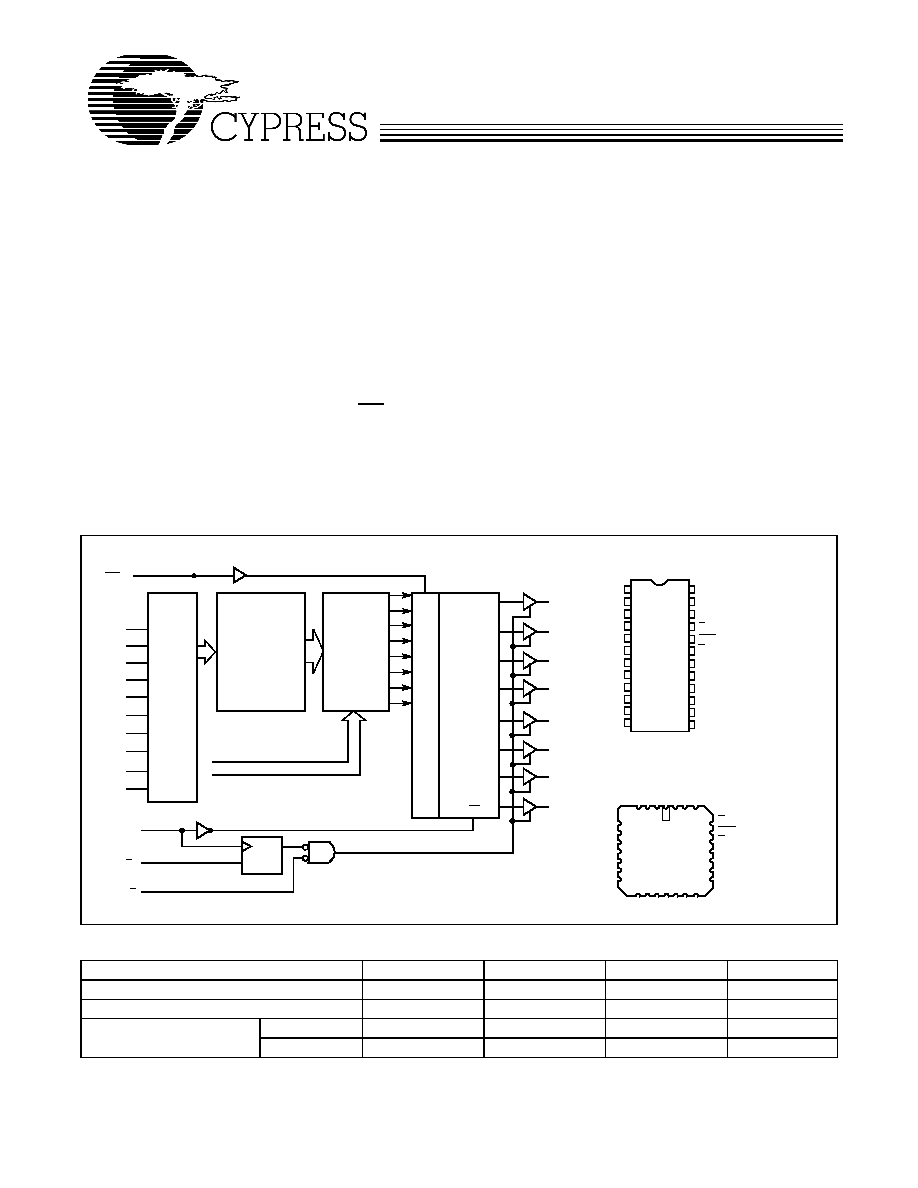
PROGRAMMABLE
ARRAY
MULTIPLEXER
COLUMN
ADDRESS
ROW
ADDRESS
15
8-BIT
EDGE-
REGISTER
TRIGGERED
O
7
O
6
O
5
O
4
O
3
O
2
O
1
O
0
CP
CP
E
S
E
E
S
28
4
5
6
7
8
9
10
3 2 1
27
1314151617
26
25
24
23
22
21
20
11
12
19
A
5
V
CC
GND
A
6
A
7
O
3
O
1
O
0
18
O
4
O
5
NC
A
0
A
4
A
3
E
NC
NC
NC
INIT
E
S
O
7
O
6
A
2
A
1
CP
O
2
A
8
A
9
INIT
INIT
IA
LIZ
E
W
O
RD
PRO
G
R
AM
M
ABL
E
A
9
DIP
LCC/PLCC
Top View
Top View
ADDRESS
DECODER
Logic Block Diagram
Pin Configuration
Selection Guide
7C235A-25
7C235A-30
7C235A-40
Unit
Minimum Address Set-Up Time
25
30
40
ns
Maximum Clock to Output
12
15
20
ns
Maximum Operating
Current
Commercial
90
90
90
mA
Military
120
mA

CY7C235A
Document #: 38-04002 Rev. *B
Page 2 of 10
Maximum Ratings
[1]
(Above which the useful life may be impaired. For user guide-
lines, not tested.)
Storage Temperature
..................................... -
65
∞
C to +150
∞
C
Ambient Temperature with
Power Applied
.................................................. -
55
∞
C to +125
∞
C
Supply Voltage to Ground Potential
(Pin 24 to Pin 12 for DIP)
.................................. -
0.5V to +7.0V
DC Voltage Applied to Outputs
in High Z State
.................................................... -
0.5V to +7.0V
DC Input Voltage
.................................................-
3.0V to +7.0V
DC Program Voltage (Pins 7, 18, 20 for DIP) ............... 13.0V
Static Discharge Voltage............................................ >2001V
(per MIL-STD-883, Method 3015)
Latch-Up Current..................................................... >200 mA
Operating Range
Range
Ambient
Temperature
V
CC
Commercial
0
∞
C to +70
∞
C
5V
±
10%
Military
[2]
-
55
∞
C to +125
∞
C
5V
±
10%
Electrical Characteristics
Over Operating Range
[3]
Parameter
Description
Test Conditions
Min.
Max.
Unit
V
OH
Output HIGH Voltage
V
CC
= Min., I
OH
=
-
4.0 mA
V
IN
= V
IH
or V
IL
2.4
V
V
OL
Output LOW Voltage
V
CC
= Min., I
OL
= 16 mA
V
IN
= V
IH
or V
IL
0.4
V
V
IH
Input HIGH
Level
Guaranteed Input Logical HIGH Voltage for All
Inputs
[4]
2.0
V
V
IL
Input LOW Level
Guaranteed Input Logical LOW Voltage for All
Inputs
[4]
0.8
V
I
IX
Input Leakage Current
GND < V
IN
< V
CC
-
10
+10
µ
A
V
CD
Input Clamp Diode Voltage
Note 5
I
OZ
Output Leakage Current
GND < V
OUT
< V
CC
Output Disabled
[4]
-
10
+10
µ
A
I
OS
Output Short Circuit Current
V
CC
= Max., V
OUT
= 0.0V
[6]
-
20
-
90
mA
I
CC
Power Supply Current
I
OUT
= 0 mA,
V
CC
= Max.
Commercial
90
mA
Military
120
V
PP
Programming Supply Voltage
12
13
V
I
PP
Programming Supply Current
50
mA
V
IHP
Input HIGH Programming Voltage
3.0
V
V
ILP
Input LOW Programming Voltage
0.4
V
Capacitance
[5]
Parameter
Description
Test Conditions
Max.
Unit
C
IN
Input Capacitance
T
A
= 25
∞
C, f = 1 MHz, V
CC
=5.0V
10
pF
C
OUT
Output Capacitance
10
pF
Notes:
1.
The volatge on any input or I/O pin cannot exceed the power pin during power-up.
2.
T
A
is the "instant on" case temperature.
3.
See the last page of this specification for Group A subgroup testing information.
4.
For devices using the synchronous enable, the device must be clocked after applying these voltages to perform this measurement.
5.
See Introduction to CMOS PROMs in this Data Book for general information on testing.
6.
For test purposes, not more than one output at a time should be shorted. Short circuit test duration should not exceed 30 seconds.

CY7C235A
Document #: 38-04002 Rev. *B
Page 3 of 10
a
Operating Modes
The CY7C235A incorporates a D-type, master-slave register
on chip, reducing the cost and size of pipelined micropro-
grammed systems and applications where accessed PROM
data is stored temporarily in a register. Additional flexibility is
provided with synchronous (E
S
) and asynchronous (E) output
enables and asynchronous initialization (INIT).
Upon power-up, the synchronous enable (ES) flip-flop will be
in the set condition causing the outputs (O
0
-
O
7
) to be in the
OFF or high-impedance state. Data is read by applying the
memory location to the address input (A
0
-
A
9
) and a logic LOW
to the enable (E
S
) input. The stored data is accessed and
loaded into the master flip-flops of the data register during the
address set-up time. At the next LOW-to-HIGH transition of the
clock (CP), data is transferred to the slave flip-flops, which
drive the output buffers, and the accessed data will appear at
the outputs (O
0
-
O
7
), provided the asynchronous enable (E) is
also LOW.
The outputs may be disabled at any time by switching the
asynchronous enable (E) to a logic HIGH, and may be
returned to the active state by switching the enable to a logic
LOW.
Regardless of the condition of E, the outputs will go to the OFF
or high-impedance state upon the next positive clock edge
after the synchronous enable (E
S
) input is switched to a HIGH
level. If the synchronous enable pin is switched to a logic LOW,
the subsequent positive clock edge will return the output to the
active state if E is LOW. Following a positive clock edge, the
address and synchronous enable inputs are free to change
since no change in the output will occur until the next
LOW-to-HIGH transition of the clock. This unique feature
allows the CY7C235A decoders and sense amplifiers to
access the next location while previously addressed data
remains stable on the outputs.
System timing is simplified in that the on-chip edge-triggered
register allows the PROM clock to be derived directly from the
system clock without introducing race conditions. The on-chip
register timing requirements are similar to those of discrete
registers available in the market.
The CY7C235A has an asynchronous initialize input (INIT).
The initialize function is useful during power-up and time-out
sequences and can facilitate implementation of other sophis-
ticated functions such as a built-in "jump start" address. When
activated the initialize control input causes the contents of a
user programmed 1025th 8-bit word to be loaded into the
on-chip register. Each bit is programmable and the initialize
function can be used to load any desired combination of 1s
and 0s into the register. In the unprogrammed state, activating
INIT will generate a register CLEAR (all outputs LOW). If all
the bits of the initialize word are programmed, activating INIT
performs a register PRESET (all outputs HIGH).
Applying a LOW to the INIT input causes an immediate load
of the programmed initialize word into the master and slave
flip-flops of the register, independent of all other inputs,
including the clock (CP). The initialize data will appear at the
device outputs after the outputs are enabled by bringing the
asynchronous enable (E) LOW.
When power is applied the (internal) synchronous enable
flip-flop will be in a state such that the outputs will be in the
high-impedance state. In order to enable the outputs, a clock
must occur and the ES input pin must be LOW at least a set-up
time prior to the clock LOW-to-HIGH transition. The E input
may then be used to enable the outputs.
When the asynchronous initialize input, INIT, is LOW, the data
in the initialize byte will be asynchronously loaded into the
output register. It will not, however, appear on the output pins
until they are enabled, as described in the preceding
paragraph.
AC Test Loads and Waveforms
[5]
3.0V
5V
OUTPUT
R1 250
R2
167
50 pF
INCLUDING
JIG AND
SCOPE
GND
90%
10%
90%
10%
5 ns
5 ns
5V
OUTPUT
5 pF
INCLUDING
JIG AND
SCOPE
(b) High-ZLoad
OUTPUT
2.0V
Equivalent to:
TH
…VENIN EQUIVALENT
100
R1 250
(a) NormalLoad
R2
167
ALL INPUT PULSES

CY7C235A
Document #: 38-04002 Rev. *B
Page 4 of 10
Switching Waveforms
[5]
Programming Information
Programming support is available from Cypress as well as
from a number of third-party software vendors. For detailed
programming information, including a listing of software
packages, please see the PROM Programming Information
located at the end of this section. Programming algorithms can
be obtained from any Cypress representative.
Switching Characteristics
Over Operating Range
[3, 5]
7C235A-25
7C235A-30
7C235A-40
Parameter
Description
Min.
Max.
Min.
Max.
Min.
Max.
Unit
t
SA
Address Set-Up to Clock HIGH
25
30
40
ns
t
HA
Address Hold from Clock HIGH
0
0
0
ns
t
CO
Clock HIGH to Valid Output
12
15
20
ns
t
PWC
Clock Pulse Width
12
15
20
ns
t
SES
E
S
Set-Up to Clock HIGH
10
10
15
ns
t
HES
E
S
Hold from Clock HIGH
5
5
5
ns
t
DI
Delay from INIT to Valid Output
25
25
35
ns
t
RI
INIT Recovery to Clock HIGH
20
20
20
ns
t
PWI
INIT Pulse Width
20
20
25
ns
t
COS
Inactive to Valid Output from Clock HIGH
[7]
20
20
25
ns
t
HZC
Inactive Output from Clock HIGH
[7]
20
20
25
ns
t
DOE
Valid Output from E LOW
20
20
25
ns
t
HZE
Inactive Output from E HIGH
20
20
25
ns
Note:
7.
Applies only when the synchronous (E
S
) function is used.
t
DI
t
CO
t
DOE
t
HZE
t
HZC
t
SA
t
HA
t
HES
t
SES
t
PWC
t
PWC
t
PWC
t
PWC
t
PWC
t
PWC
t
HA
t
CO
t
COS
O
0
-
O
7
A
0
-
A
10
INIT
CP
E
S
E
t
RI
t
PWI
t
HES
t
SES
t
HES
t
SES

CY7C235A
Document #: 38-04002 Rev. *B
Page 5 of 10
Table 1. Mode Selection
Pin Function
[8]
Read or Output Disable
A
0
, A
3
-
A
9
A
1
A
2
CP
E
S
E
INIT
O
7
-
O
0
Mode
Other
A
0
, A
3
-
A
9
A
1
A
2
PGM
VFY
E
V
PP
D
7
-
D
0
Read
A
0
, A
3
-
A
9
A
1
A
2
X
V
IL
V
IL
V
IH
O
7
-
O
0
Output Disable
A
0
, A
3
-
A
9
A
1
A
2
X
V
IH
X
V
IH
High Z
Output Disable
A
0
, A
3
-
A
9
A
1
A
2
X
X
V
IH
V
IH
High Z
Initialize
A
0
, A
3
-
A
9
A
1
A
2
X
X
V
IL
V
IL
Init Byte
Program
A
0
, A
3
-
A
9
A
1
A
2
V
ILP
V
IHP
V
IHP
V
PP
D
7
-
D
0
Program Verify
A
0
, A
3
-
A
9
A
1
A
2
V
IHP
V
ILP
V
IHP
V
PP
O
7
-
O
0
Program Inhibit
A
0
, A
3
-
A
9
A
1
A
2
V
IHP
V
IHP
V
IHP
V
PP
High Z
Intelligent Program
A
0
, A
3
-
A
9
A
1
A
2
V
ILP
V
IHP
V
IHP
V
PP
D
7
-
D
0
Program Initialize Byte
A
0
, A
3
-
A
9
V
PP
V
ILP
V
ILP
V
IHP
V
IHP
V
PP
D
7
-
D
0
Blank Check
A
0
, A
3
-
A
9
A
1
A
2
V
IHP
V
ILP
V
IHP
V
PP
Zeros
Note:
8.
X = "don't care" but not to exceed V
CC
±5%.
Figure 1. Programming Pinouts
1
2
3
4
5
6
7
8
9
10
11
12
16
17
18
19
20
24
23
22
21
13
14
A
8
A
7
A
6
A
5
A
4
A
3
A
2
A
1
A
0
D
0
D
1
D
2
GND
V
CC
D
7
D
6
D
4
D
5
D
3
15
A
9
E
V
PP
VFY
PGM
28
4
5
6
7
8
9
10
3 2 1
27
1314151617
26
25
24
23
22
21
20
11
12
19
A
5
V CC
GND
A
6
A
7
D
3
D
1
D
0
18
D
4
D
5
NC
A
0
A
4
A
3
A
8
NC
NC
D
7
D
6
A
2
A
1
D
2
E
V
PP
VFY
PGM
NC
A
9
DIP
LCC/PLCC
Top View
Top View

CY7C235A
Document #: 38-04002 Rev. *B
Page 6 of 10
Typical DC and AC Characteristics
1.4
1.6
1.0
0.8
4.0
4.5
5.0
5.5
6.0
-
55
25
125
1.2
1.1
1.6
4.0
4.5
5.0
5.5
6.0
N
O
R
M
AL
IZ
ED
C
L
O
C
K
-
T
O
-O
U
T
PU
T
TI
ME
SUPPLY VOLTAGE (V)
NORMALIZED SUPPLY CURRENT
vs. SUPPLY VOLTAGE
NORMALIZED SUPPLY CURRENT
vs. AMBIENT TEMPERATURE
AMBIENT TEMPERATURE (
∞
C)
SUPPLY VOLTAGE (V)
CLOCK TO OUTPUT TIME
vs. V
CC
0.6
1.2
1.6
1.4
1.2
1.0
0.8
-
55
125
NORMA
L
I
Z
E
D
S
E
T
-
UP
T
I
ME
AMBIENT TEMPERATURE (
∞
C)
CLOCK TO OUTPUT TIME
vs. TEMPERATURE
150
175
125
75
50
25
0.0
1.0
2.0
3.0
OUT
P
U
T
S
I
NK
CURRE
NT
(m
A
)
0
100
OUTPUT VOLTAGE (V)
OUTPUT SINK CURRENT
vs. OUTPUT VOLTAGE
1.0
0.9
0.8
NO
RM
A
L
I
Z
E
D
I
CC
NORM
A
L
IZ
E
D
I
CC
V
CC
=5.0V
T
A
=25
∞
C
T
A
=25
∞
C
0.6
0.6
1.02
1.00
0.98
0.96
0.94
0.92
0
25
50
75
CLOCK PERIOD (ns)
30.0
25.0
20.0
15.0
10.0
5.0
0
200
400
600
800
D
E
L
T
A t
(
n
s
)
AA
CAPACITANCE (pF)
TYPICAL ACCESS TIME CHANGE
vs. OUTPUT LOADING
100
0.0
1000
T
A
=25
∞
C
V
CC
=4.5V
T
A
=25
∞
C
f = f
MAX
25
0.88
NORMALIZED SUPPLY CURRENT
vs. CLOCK PERIOD
4.0
1.4
1.2
1.0
0.8
1.6
1.4
1.2
1.0
0.8
-
55
125
N
O
R
M
ALI
Z
ED
SE
T
-
U
P
0.6
25
AMBIENT TEMPERATURE (
∞
C)
NORMALIZED SET-UP TIME
vs. TEMPERATURE
1.2
4.0
4.5
5.0
5.5
6.0
NORMA
L
I
Z
E
D
CLOCK
-
T
O
-OUT
P
U
T
T
I
ME
0.4
SUPPLY VOLTAGE (V)
NORMALIZED SET-UP TIME
vs. SUPPLY VOLTAGE
T
A
=25
∞
C
1.0
0.8
0.6
C235A-10
NORM
A
L
IZ
E
D
I
CC
0.90
V
CC
=5.5V
T
A
=25
∞
C

CY7C235A
Document #: 38-04002 Rev. *B
Page 7 of 10
MILITARY SPECIFICATIONS
Group A Subgroup Testing
Ordering Information
Speed
(ns)
Package
Name
Operating Range
t
SA
t
CO
Ordering Code
Package Type
25
12 CY7C235A-25PC
P13
24-Lead (300-Mil) Molded DIP
Commercial
30
15 CY7C235A-30JC
J64
28-Lead Plastic Leaded Chip Carrier
40
20 CY7C235A-40PC
P13
24-Lead (300-Mil) Molded DIP
CY7C235A-40DMB
D14
24-Lead (300-Mil) CerDIP
Military
CY7C235A-40LMB
L64
28-Square Leadless Chip Carrier
DC Characteristics
Parameter
Subgroups
V
OH
1, 2, 3
V
OL
1, 2, 3
V
IH
1, 2, 3
V
IL
1, 2, 3
I
IX
1, 2, 3
I
OZ
1, 2, 3
I
CC
1, 2, 3
Switching Characteristics
Parameter
Subgroups
t
SA
7, 8, 9, 10, 11
t
HA
7, 8, 9, 10, 11
t
CO
7, 8, 9, 10, 11
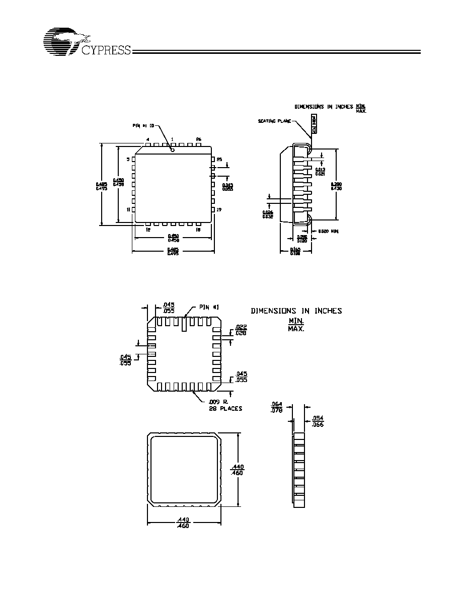
Package Diagrams
24-Lead (300-Mil) CerDIP D14
MIL-STD-1835 D- 9 Config.A
51-80031-**
CY7C235A
Document #: 38-04002 Rev. *B
Page 8 of 10
Package Diagrams
(continued)
28-Lead Plastic Leaded Chip Carrier J64
51-85001-*A
28-Square Leadless Chip Carrier L64
MIL-STD-1835 C-4
51-80051-**

CY7C235A
Document #: 38-04002 Rev. *B
Page 9 of 10
© Cypress Semiconductor Corporation, 2002. The information contained herein is subject to change without notice. Cypress Semiconductor Corporation assumes no responsibility for the use
of any circuitry other than circuitry embodied in a Cypress Semiconductor product. Nor does it convey or imply any license under patent or other rights. Cypress Semiconductor does not authorize
its products for use as critical components in life-support systems where a malfunction or failure may reasonably be expected to result in significant injury to the user. The inclusion of Cypress
Semiconductor products in life-support systems application implies that the manufacturer assumes all risk of such use and in doing so indemnifies Cypress Semiconductor against all charges.
All product and company names mentioned in this document may be the trademarks of their respective holders.
Package Diagrams
(continued)
51-85013-A
24-Lead (300-Mil) Molded DIP P13

CY7C235A
Document #: 38-04002 Rev. *B
Page 10 of 10
Document History Page
Document Title: CY7C235A 1K x 8 Registered PROM
Document Number: 38-04002
REV.
ECN NO.
Issue
Date
Orig. of
Change
Description of Change
**
113857
03/06/02
DSG
Change from Spec number: 38-00229 to 38-04002
*A
118893
10/09/02
GBI
Update ordering information
*B
122243
12/27/02
RBI
Add power up requirements to maximum ratings information.