
192-Macrocell MAX
Æ
EPLD
CY7C341
Cypress Semiconductor Corporation
∑
3901 North First Street
∑
San Jose
∑
CA 95134
∑
408-943-2600
Document #: 38-03034 Rev. *A
Revised December 11, 2001
41
Features
∑ 192 macrocells in 12 logic array blocks (LABs)
∑ Eight dedicated inputs, 64 bidirectional I/O pins
∑ 0.8-micron double-metal CMOS EPROM technology
∑ Programmable interconnect array
∑ 384 expander product terms
∑ Available in 84-pin HLCC, PLCC, and PGA packages
Functional Description
The CY7C341 is an Erasable Programmable Logic Device
(EPLD) in which CMOS EPROM cells are used to configure
logic functions within the device. The MAX
Æ
architecture is
100% user-configurable, allowing the devices to accom-
modate a variety of independent logic functions.
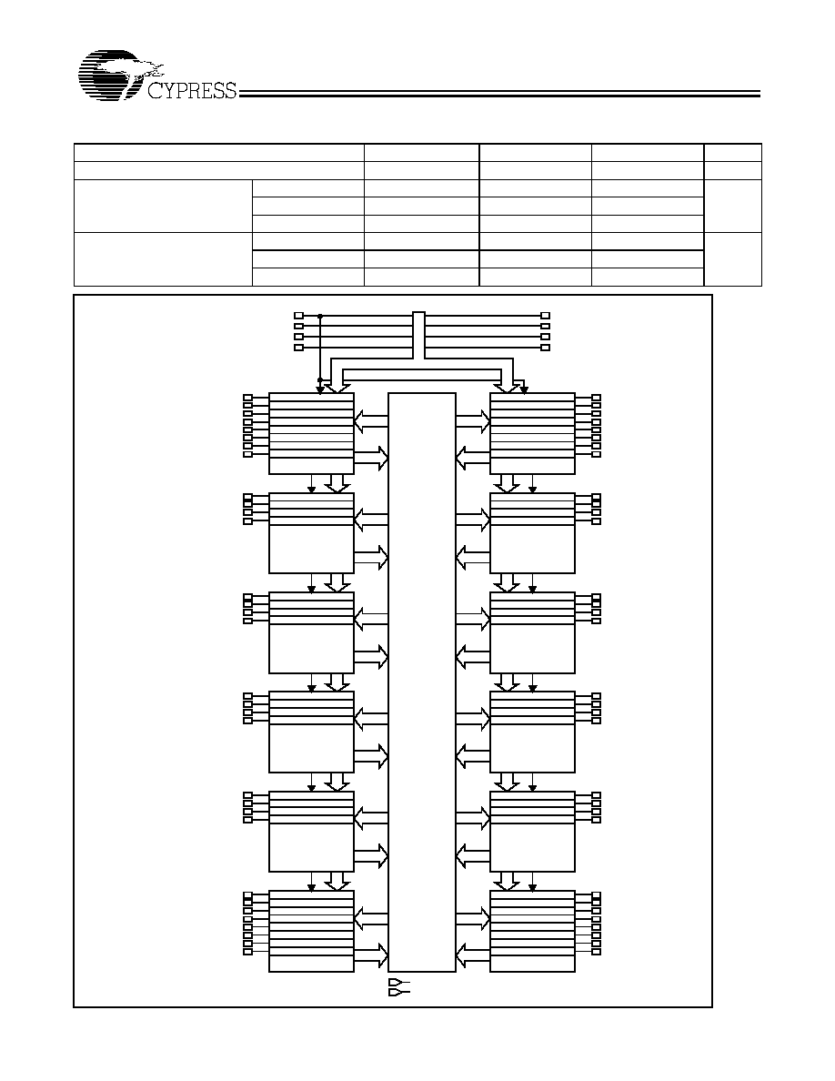
The 192 macrocells in the CY7C341 are divided into 12 LABs,
16 per LAB. There are 384 expander product terms, 32 per
LAB, to be used and shared by the macrocells within each
LAB. Each LAB is interconnected with a programmable inter-
connect array, allowing all signals to be routed throughout the
chip.
The speed and density of the CY7C341 allows them to be
used in a wide range of applications, from replacement of large
amounts of 7400-series TTL logic, to complex controllers and
multifunction chips. With greater than 37 times the function-
ality of 20-pin PLDs, the CY7C341 allows the replacement of
over 75 TTL devices. By replacing large amounts of logic, the
CY7C341 reduces board space and part count, and increases
system reliability.
Each LAB contains 16 macrocells. In LABs A, F, G, and L, eight
macrocells are connected to I/O pins and eight are buried,
while for LABs B, C, D, E, H, I, J, and K, four macrocells are
connected to I/O pins and 12 are buried. Moreover, in addition
to the I/O and buried macrocells, there are 32 single product
term logic expanders in each LAB. Their use greatly enhances
the capability of the macrocells without increasing the number
of product terms in each macrocell.
Logic Array Blocks
There are 12 logic array blocks in the CY7C341. Each LAB
consists of a macrocell array containing 16 macrocells, an
expander product term array containing 32 expanders, and an
I/O block. The LAB is fed by the programmable interconnect
array and the dedicated input bus. All macrocell feedbacks go
to the macrocell array, the expander array, and the program-
mable interconnect array. Expanders feed themselves and the
macrocell array. All I/O feedbacks go to the programmable
interconnect array so that they may be accessed by macro-
cells in other LABs as well as the macrocells in the LAB in
which they are situated.
Externally, the CY7C341 provides eight dedicated inputs, one
of which may be used as a system clock. There are 64 I/O pins
that may be individually configured for input, output, or bidirec-
tional data flow.
Programmable Interconnect Array
The Programmable Interconnect Array (PIA) solves inter-
connect limitations by routing only the signals needed by each
logic array block. The inputs to the PIA are the outputs of every
macrocell within the device and the I/O pin feedback of every
pin on the device.
Unlike masked or programmable gate arrays, which induce
variable delay dependent on routing, the PIA has a fixed delay.
This eliminates undesired skews among logic signals, which
may cause glitches in internal or external logic. The fixed
delay, regardless of programmable interconnect array config-
uration, simplifies design by assuring that internal signal
skews or races are avoided. The result is ease of design imple-
mentation, often in a single pass, without the multiple internal
logic placement and routing iterations required for a program-
mable gate array to achieve design timing objectives.
Timing Delays
Timing delays within the CY7C341 may be easily determined
using WarpTM, Warp ProfessionalTM, or Warp EnterpriseTM
software. The CY7C341 has fixed internal delays, allowing the
user to determine the worst case timing delays for any design.
Design Recommendations
For proper operation, input and output pins must be
constrained to the range GND < (V
IN
or V
OUT
) < V
CC
. Unused
inputs must always be tied to an appropriate logic level (either
V
CC
or GND). Each set of V
CC
and GND pins must be
connected together directly at the device. Power supply
decoupling capacitors of at least 0.2
µ
F must be connected
between V
CC
and GND. For the most effective decoupling,
each V
CC
pin should be separately decoupled to GND, directly
at the device. Decoupling capacitors should have good
frequency response, such as monolithic ceramic types.
Design Security
The CY7C341 contains a programmable design security
feature that controls the access to the data programmed into
the device. If this programmable feature is used, a proprietary
design implemented in the device cannot be copied or
retrieved. This enables a high level of design control to be
obtained since programmed data within EPROM cells is
invisible. The bit that controls this function, along with all other
program data, may be reset simply by erasing the device. The
CY7C341 is fully functionally tested and guaranteed through
complete testing of each programmable EPROM bit and all internal
logic elements thus ensuring 100% programming yield.
The erasable nature of these devices allows test programs to
be used and erased during early stages of the production flow.
The devices also contain on-board logic test circuitry to allow
verification of function and AC specification once encapsu-
lated in non-windowed packages.
CY7C341
Document #: 38-03034 Rev. *A
Page 2 of 15
Selection Guide
7C341-25
7C341-30
7C341-35
Unit
Maximum Access Time
25
30
35
ns
Maximum Operating Current
Commercial
380
380
380
mA
Industrial
480
480
480
Military
480
480
480
Maximum Standby Current
Commercial
360
360
360
mA
Industrial
435
435
435
Military
435
435
435
P
I
A
MACROCELL 1
MACROCELL 2
MACROCELL 3
MACROCELL 4
MACROCELL 5
MACROCELL 6
MACROCELL 7
MACROCELL 8
MACROCELL 97
MACROCELL 98
MACROCELL 99
MACROCELL 100
MACROCELL 101
MACROCELL 102
MACROCELL 103
MACROCELL 104
MACROCELL 9≠16
MACROCELL 105≠112
MACROCELL 17
MACROCELL 18
MACROCELL 19
MACROCELL 20
MACROCELL 113
MACROCELL 114
MACROCELL 115
MACROCELL 116
MACROCELL 21≠32
MACROCELL 117≠128
MACROCELL 33
MACROCELL 34
MACROCELL 35
MACROCELL 36
MACROCELL 129
MACROCELL 130
MACROCELL 131
MACROCELL 132
MACROCELL 37≠48
MACROCELL 133≠144
MACROCELL 49
MACROCELL 50
MACROCELL 51
MACROCELL 52
MACROCELL 145
MACROCELL 146
MACROCELL 147
MACROCELL 148
MACROCELL 53≠64
MACROCELL 149≠160
MACROCELL 65
MACROCELL 66
MACROCELL 67
MACROCELL 68
MACROCELL 161
MACROCELL 162
MACROCELL 163
MACROCELL 164
MACROCELL 69≠80
MACROCELL 165≠176
MACROCELL 81
MACROCELL 82
MACROCELL 83
MACROCELL 84
MACROCELL 85
MACROCELL 86
MACROCELL 87
MACROCELL 88
MACROCELL 177
MACROCELL 178
MACROCELL 179
MACROCELL 180
MACROCELL 181
MACROCELL 182
MACROCELL 183
MACROCELL 184
MACROCELL 89≠96
MACROCELL 185≠192
INPUT
(C6) 84
INPUT
(C7) 83
INPUT
(L7) 44
INPUT
(J7) 43
1 (A6)
INPUT/CLK
2 (A5)
INPUT
41 (K6)
INPUT
42 (J6)
INPUT
4
(C5)
5
(A4)
6
(B4)
7
(A3)
8
(A2)
9
(B3)
10
(A1)
11
(B2)
12 (C2)
13 (B1)
14 (C1)
15 (D2)
16
(D1)
17
(E3)
20
(F2)
21
(F3)
22 (G3)
23 (G1)
25
(F1)
26
(H1)
27
(H2)
28
(J1)
29
(K1)
30
(J2)
31
(L1)
32
(K2)
33
(K3)
34
(L2)
35
(L3)
36
(K4)
37
(L4)
38
(J5)
46 (L6)
47 (L8)
48 (K8)
49 (L9)
50 (L10)
51 (K9)
52 (L11)
53 (K10)
54 (J10)
55 (K11)
56 (J11)
57 (H10)
58 (H11)
59 (F10)
62 (G9)
63 (F9)
64 (F11)
65 (E11)
67 (E9)
68 (D11)
69 (D10)
70 (C11)
71 (B11)
72 (C10)
73 (A11)
74 (B10)
75 (B9)
76 (A10)
77 (A9)
78 (B8)
79 (A8)
80 (B6)
SYSTEMCLOCK
3, 24, 45, 66 (B5, G2, K7, E10)
18, 19, 39, 40, 60, 61, 81, 82 (E1, E2, K5, L5, G10, G11, A7, B7)
V
CC
GND
() ≠ PERTAIN TO 84-PIN PGA PACKAGE
LAB A
LAB B
LAB C
LAB D
LAB E
LAB F
LAB G
LAB H
LAB I
LAB J
LAB K
LAB L
C341-1
Logic Block Diagram

CY7C341
Document #: 38-03034 Rev. *A
Page 3 of 15
Pin Configurations
I/O
Top View
PLCC/HLCC
9 8
6
7
5
13
14
12
11 10
49
48
58
59
60
23
24
26
25
27
15
16
47
46
4 3
28
33
20
21
19
18
17
22
34 35
37
36
38 39
42
41
43 44 45
40
66
65
63
64
62
61
V
CC
7C341
C341-2
67
68
69
74
72
73
71
70
84 83
81
82
80
2 1
79
I/O
INP
U
T
I/O
INP
U
T
/
CLK
INP
U
T
INP
U
T
GND
GND
I/O
I/O
I/O
I/O
I/O
I/O
I/O
I/O
I/O
I/O
I/O
I/O
I/O
I/O
I/O
I/O
GND
I/O
I/O
I/O
I/O
V
CC
V
CC
INP
U
T
GND
GND
INP
U
T
I/O
I/O
I/O
I/O
I/O
I/O
I/O
I/O
I/O
I/O
I/O
I/O
I/O
I/O
I/O
I/O
I/O
I/O
GND
I/O
V
CC
I/O
I/O
I/O
I/O
I/O
I/O
I/O
I/O
I/O
I/O
V
CC
INPUT
INPUT/
CLK
GND
I/O
I/O
I/O
I/O
V
CC
I/O
I/O
I/O
GND
GND
I/O
I/O
I/O
I/O
I/O
I/O
I/O
I/O
I/O
I/O
I/O
V
CC
INPUT
I/O
GND
GND
I/O
I/O
I/O
I/O
I/O
I/O
I/O
I/O
I/O
I/O
V
CC
I/O
I/O
I/O
GND
GND
I/O
I/O
I/O
I/O
I/O
I/O
PGA
Bottom View
7C341
C341-3
INPUT
GND
I/O
I/O
I/O
I/O
I/O
I/O
I/O
L
K
J
H
G
F
E
D
C
B
A
1
2
3
4
5
6
7
8
9
10
11
I/O
I/O
I/O
I/O
I/O
INPUT INPUT
INPUT
INPUT
I/O
I/O
I/O
I/O
I/O
I/O
I/O
I/O
53
52
51
50
30
29
31
32
I/O
I/O
I/O
I/O
I/O
I/O
I/O
I/O
54
55
56
57
I/O
I/O
I/O
I/O
77
78
76 75
I/O
I/O
I/O
I/O
I/O
GND
INP
U
T
INP
U
T
GND
I/O
Figure 1. CY7C341 Internal Timing Model
LOGIC ARRAY
CONTROL DELAY
t
LAC
EXPANDER
DELAY
t
EXP
CLOCK
DELAY
t
IC
t
RD
t
COMB
t
LATCH
INPUT
DELAY
t
IN
PIA
DELAY
t
PIA
REGISTER
OUTPUT
DELAY
t
OD
t
XZ
t
ZX
LOGIC ARRAY
DELAY
t
LAD
LOGIC ARRAY
DELAY
t
FD
I/O DELAY
t
IO
INPUT/
OUTPUT
INPUT
C341-4
SYSTEM CLOCK DELAY t
ICS
t
RH
t
RSU
t
PRE
t
CLR

CY7C341
Document #: 38-03034 Rev. *A
Page 4 of 15
Maximum Ratings
(Above which the useful life may be impaired. For user guide-
lines, not tested.)
Storage Temperature
.......................................-
65
∞
C to +150
∞
C
Ambient Temperature with
Power Applied.................................................... 0
∞
C to +70
∞
C
Maximum Junction Temperature
(Under Bias)................................................................. 150
∞
C
Supply Voltage to Ground Potential
.................-
2.0V to +7.0V
Maximum Power Dissipation...................................2500 mW
DC V
CC
or GND Current......................................................500 mA
DC Output Current, per Pin
........................ -
25 mA to +25 mA
DC Input Voltage
[1]
................................................-
3.0V to +7.0V
DC Program Voltage .................................................... 13.0V
Static Discharge Voltage
..................................................>
1100V
(per MIL-STD-883, method 3015)
Operating Range
Range
Ambient Temperature
V
CC
Commercial
0
∞
C to +70
∞
C
5V
±
5%
Industrial
≠40
∞
C to +85
∞
C
5V
±
10%
Military
≠55
∞
C to +125
∞
C (Case)
5V
±
10%
Electrical Characteristics
Over the Operating Range
[2]
Parameter
Description
Test Conditions
Min.
Max.
Unit
V
OH
Output HIGH Voltage
V
CC
= Min., I
OH
= ≠4.0 mA
2.4
V
V
OL
Output LOW Voltage
V
CC
= Min., I
OL
= 8 mA
0.45
V
V
IH
Input HIGH Level
2.2
V
CC
+ 0.3
V
V
IL
Input LOW Level
-
0.3
0.8
V
I
IX
Input Current
GND
V
IN
V
CC
-
10
+10
µ
A
I
OZ
Output Leakage Current V
O
= V
CC
or GND
-
40
+40
µ
A
I
OS
Output Short
Circuit Current
V
CC
= Max., V
OUT
= GND
[3, 4]
-
30
-
90
mA
I
CC1
Power Supply Current
(Standby)
V
I
= V
CC
or GND (No Load)
Commercial
360
mA
Military/Industrial
435
mA
I
CC2
Power Supply Current
[5]
V
I
= V
CC
or GND (No Load)
f = 1.0 MHz
[3, 5]
Commercial
380
mA
Military/Industrial
480
mA
t
R
(Recom-
mended)
Input Rise Time
100
ns
t
F
(Recom-
mended)
Input Fall Time
100
ns
Capacitance
[6]
Parameter
Description
Test Conditions
Max.
Unit
C
IN
Input Capacitance
T
A
= 25
∞
C, f = 1 MHz, V
CC
= 5.0V
10
pF
C
OUT
Output Capacitance
20
pF
Notes:
1.
Minimum DC input is ≠0.3V. During transitions, the inputs may undershoot to ≠2.0V for periods less than 20 ns.
2.
Typical values are for T
A
= 25
∞
C and V
CC
= 5V.
3.
Guaranteed but not 100% tested.
4.
No more than one output should be tested at a time. Duration of the short circuit should not be more than one second. V
OUT
= 0.5V has been chosen to avoid
test problems caused by tester ground degradation.
5.
This parameter is measured with device programmed as a 16-bit counter in each LAB and is tested periodically by sampling production material.
6.
Part (a) in AC Test Load and Waveforms is used for all parameters except t
ER
and t
XZ
, which is used for part (b) in AC Test Load and Waveforms. All external timing
parameters are measured referenced to external pins of the device.

CY7C341
Document #: 38-03034 Rev. *A
Page 5 of 15
AC Test Loads and Waveforms
3.0V
5V
OUTPUT
R1 464
R2
250
50 pF
INCLUDING
JIG AND
SCOPE
GND
90%
10%
90%
10%
< 6 ns
< 6 ns
5V
OUTPUT
R1 464
R2
250
(a)
(b)
OUTPUT
1.75V
Equivalent to:
TH…
VENIN EQUIVALENT (commercial/military)
C341-5
C341-6
ALL INPUT PULSES
t
R
t
F
5 pF
163
External Synchronous Switching Characteristics Over the Operating Range
[6]
Parameter
Description
7C341-25
7C341-30
7C341-35
Min.
Max
Min.
Max
Min.
Max
Unit
t
PD1
Dedicated Input to Combinatorial
Output Delay
[7]
Com'l
25
30
35
ns
Mil
25
30
35
t
PD2
I/O Input to Combinatorial
Output Delay
[8]
Com'l
40
45
55
ns
Mil
40
45
55
t
PD3
Dedicated Input to Combinatorial
Output Delay with Expander Delay
[9]
Com'l
37
44
55
ns
Mil
37
44
55
t
PD4
I/O Input to Combinatorial Output
Delay with Expander Delay
[3, 10]
Com'l
52
59
75
ns
Mil
52
59
75
t
EA
Input to Output Enable Delay
[3, 7]
Com'l
25
30
35
ns
Mil
25
30
35
t
ER
Input to Output Disable Delay
[6]
Com'l
25
30
35
ns
Mil
25
30
35
t
CO1
Synchronous Clock Input to
Output Delay
Com'l
14
16
20
ns
Mil
14
16
20
t
CO2
Synchronous Clock to Local
Feedback to Combinatorial
Output
[3, 11]
Com'l
30
35
42
ns
Mil
30
35
42
t
S1
Dedicated Input or Feedback Set-up
Time to Synchronous Clock
Output
[6, 12]
Com'l
15
20
25
ns
Mil
15
20
25
t
S2
I/O Input Set-up Time to
Synchronous Clock Input
[8]
Com'l
30
39
45
ns
Mil
30
39
45
Notes:
7.
This specification is a measure of the delay from input signal applied to a dedicated input to combinatorial output on any output pin. This delay assumes that
no expander terms are used to form the logic function. When this note is applied to any parameter specification it indicates that the signal (data, asynchronous
clock, asynchronous clear, and/or asynchronous preset) is applied to a dedicated input only and no signal path (either clock or data) employs expander logic.
If an input signal is applied to an I/O pin an additional delay equal to t
PIA
should be added to the comparable delay for a dedicated input. If expanders are used, add the
maximum expander delay t
EXP
to the overall delay for the comparable delay without expanders.
8.
This specification is a measure of the delay from input signal applied to an I/O macrocell pin to any output. This delay assumes no expander terms are used
to form the logic function.
9.
This specification is a measure of the delay from an input signal applied to a dedicated input to combinatorial output on any output pin. This delay assumes
expander terms are used to form the logic functions and includes the worst-case expander logic delay for one pass through the expander logic.
10. This specification is a measure of the delay from an input signal applied to an I/O macrocell pin to any output. This delay assumes expander terms are used
to form the logic function and includes the worst-case expander logic delay for one pass through the expander logic. This parameter is tested periodically by
sampling production material.
11. This specification is a measure of the delay from synchronous register clock to internal feedback of the register output signal to the input of the LAB logic array
and then to a combinatorial output. This delay assumes no expanders are used, register is synchronously clocked and all feedback is within the same LAB.
This parameter is tested periodically by sampling production material.
12. If data is applied to an I/O input for capture by a macrocell register, the I/O pin set-up time minimums should be observed. These parameters are t
S2
for
synchronous operation and t
AS2
for asynchronous operation.