
PRELIMINARY
256K x 16 Static RAM
CY7C1041AV33/
GVT73256A16
Cypress Semiconductor Corporation
∑
3901 North First Street
∑
San Jose
∑
CA 95134
∑
408-943-2600
June 15, 2000
33
Features
∑ Fast access times: 10, 12 ns
∑ Fast OE access times: 5, 6, and 7 ns
∑ Single +3.3V ±0.3V power supply
∑ Fully static--no clock or timing strobes necessary
∑ All inputs and outputs are TTL-compatible
∑ Three state outputs
∑ Center power and ground pins for greater noise
immunity
∑ Easy memory expansion with CE and OE options
∑ Automatic CE power-down
∑ High-performance, low power consumption, CMOS
double-poly, double-metal process
∑ Packaged in 44-pin, 400-mil SOJ and 44-pin, 400-mil
TSOP
Functional Description
The CY7C1049AV33\GVT73512A8 is organized as a 262,144
x 16 SRAM using a four-transistor memory cell with a high-per-
formance, silicon gate, low-power CMOS process. Cypress
SRAMs are fabricated using double-layer polysilicon, dou-
ble-layer metal technology.
This device offers center power and ground pins for improved
performance and noise immunity. Static design eliminates the
need for external clocks or timing strobes. For increased sys-
tem flexibility and eliminating bus contention problems, this de-
vice offers Chip Enable (CE), separate Byte Enable controls
(BLE and BHE) and Output Enable (OE) with this organization.
The device offers a low-power standby mode when chip is not
selected. This allows system designers to meet low standby
power requirements.
Functional Block Diagram
CE#
ADDRESS BUFFER
ROW DECODER
COLUMN DECODER
MEMORY ARRAY
512 ROWS X 256 X 16
COLUMNS
I/O CONTROL
WE#
OE#
DQ8
DQ1
POWER
DOWN
A16
A0
DQ16
DQ9
BHE#
BLE#
VCC
VSS
Top View
SOJ/TSOP II
WE
1
2
3
4
5
6
7
8
9
10
11
14
31
32
36
35
34
33
37
40
39
38
12
13
41
44
43
42
16
15
29
30
V
CC
A
5
A
6
A
7
A
8
A
0
A
1
OE
V
SS
A
17
DQ
16
A
2
CE
DQ
3
DQ
1
DQ
2
BHE
A
3
A
4
18
17
20
19
DQ
4
27
28
25
26
22
21
23
24
V
SS
A
16
A
15
BLE
V
CC
DQ
15
DQ
14
DQ
13
DQ
12
DQ
11
DQ
10
DQ
9
A
14
A
13
A
12
A
11
A
9
A
10
NC
DQ
5
DQ
6
DQ
7
DQ
8
Pin Configuration
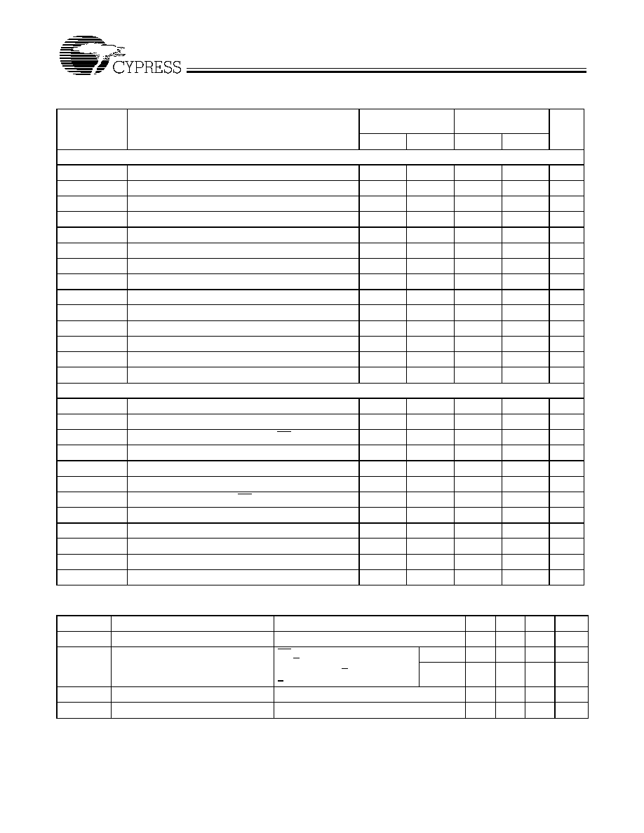
Selection Guide
CY7C1049AV33-10/
GVT73512A8-10
CY7C1049AV33-12/
GVT73512A8-12
Maximum Access Time (ns)
10
12
Maximum Operating Current (mA)
240
210
Maximum CMOS Standby Current (mA)
Com'l/Ind'l
10
10
Com'l
L
3.0
3.0

CY7C1041AV33/
GVT73256A16
PRELIMINARY
2
Maximum Ratings
(Above which the useful life may be impaired. For user guide-
lines, not tested.)
Voltage on V
CC
Supply Relative to V
SS
......... ≠0.5V to +4.6V
V
IN
...........................................................≠0.5V to V
CC
+0.5V
Storage Temperature (plastic)........................≠55∞C to +125∞
Junction Temperature ..................................................+125∞
Power Dissipation ......................................................... 1.0W
Short Circuit Output Current ....................................... 50 mA
Note:
1.
T
A
is the "Instant On" case temperature.
Truth Table
Mode
CE
WE
OE
BLE
BHE
DQ
1
≠D
8
DQ
9
≠D
16
POWER
Low Byte Read (DQ
1
≠DQ
8
)
L
H
L
L
H
Q
High-Z
Active
High Byte Read (DQ
9
≠DQ
16
)
L
H
L
H
L
High-Z
Q
Active
Word Read (DQ
1
≠DQ
16
)
L
H
L
L
L
Q
Q
Active
Low Byte Write (DQ
1
≠DQ
8
)
L
L
X
L
H
D
High-Z
Active
High Byte Write (DQ
9
≠DQ
16
)
L
L
X
H
L
High-Z
D
Active
Word Write (DQ
1
≠DQ
16
)
L
L
X
L
L
D
D
Active
Output Disable
L
X
X
H
H
High-Z
High-Z
Active
L
H
H
X
X
High-Z
High-Z
Active
Standby
H
X
X
X
X
High-Z
High-Z
Standby
Pin Descriptions
SOJ & TSOP
Pin Numbers
Pin Name
Type
Description
1, 2, 3, 4, 5, 18, 19,
20, 21, 22, 23, 24, 25,
26, 27, 42, 43, 44
A
0
≠A
17
Input
Addresses Inputs: These inputs determine which cell is addressed.
17
WE
Input
Write Enable: This input determines if the cycle is a READ or WRITE cycle. WE
is LOW for a WRITE cycle and HIGH for a READ cycle.
6
CE
Input
Chip Enable: This active LOW input is used to enable the device. When CE is
LOW, the chip is selected. When CE is HIGH, the chip is disabled and automati-
cally goes into standby power mode.
39, 40
BLE, BHE
Input
Byte Enable: These active LOW inputs allow individual bytes to be written or read.
When BLE is LOW, the data is written to or read from the lower byte (DQ
1
≠DQ
8
).
When BHE is LOW, the data is written to or read from the higher byte (DQ
9
≠DQ
16
).
41
OE
Input
Output Enable: This active LOW input enables the output drivers.
7, 8, 9, 10, 13, 14,
15, 16, 29, 30, 31, 32,
35, 36, 37, 38
DQ
1
≠DQ
16
Input/
Output
SRAM Data I/O: Data inputs and data outputs. Lower byte is DQ
1
≠DQ
8
and upper
byte is DQ
9
≠DQ
16
.
11, 33
V
CC
Supply
Power Supply: 3.3V ±0.3V%.
12, 34
V
SS
Supply
Ground.
Operating Range
Range
Ambient
Temperature
[1]
V
CC
Commercial
0
∞
C to +70
∞
C
3.3V
±
0.3V
Industrial
≠40
∞
C to +85
∞
C

CY7C1041AV33/
GVT73256A16
PRELIMINARY
3
Electrical Characteristics
Over the Operating Range
Parameter
Description
Conditions
Min.
Max.
Unit
V
IH
Input High (Logic 1) Voltage
[2, 3]
2.2
V
CC
+0.5
V
V
Il
Input Low (Logic 0) Voltage
[2, 3]
≠0.5
0.8
V
IL
I
Input Leakage Current
0V <
V
IN
< V
CC
≠5
5
µ
A
IL
O
Output Leakage Current
Output(s) disabled, 0V < V
OUT
< V
CC
≠5
5
µ
A
V
OH
Output High Voltage
[2]
I
OH
= ≠4.0 mA
2.4
V
V
OL
Output Low Voltage
[2]
I
OL
= 8.0 mA
0.4
V
V
CC
Supply Voltage
[2]
3.0
3.6
V
Parameter
Description
Conditions
Power
Typ.
-10
-12
Unit
I
CC
Power Supply
Current: Operating
[4, 5]
Device selected; CE < V
IL
; V
CC
= Max.;
f = f
MAX
; outputs open
std.
90
240
210
mA
low
240
210
I
SB1
TTL Standby
[5]
CE > V
IH
; V
CC
= Max.; f = f
MAX
std.
25
70
60
mA
low
70
60
I
SB2
CMOS Standby
[5]
CE1 > V
CC
≠ 0.2; V
CC
= Max.;
all other inputs < V
SS
+ 0.2 or > V
CC
≠ 0.2;
all inputs static; f = 0
std.
0.1
10
10
mA
low
3.0
3.0
Capacitance
[6]
Parameter
Description
Test Conditions
Max.
Unit
C
I
Input Capacitance
T
A
= 25
∞
C, f = 1 MHz,
V
CC
= 3.3V
6
pF
C
I/O
Input/Output Capacitance
(DQ)
8
pF
Note:
2.
All voltages referenced to V
SS
(GND).
3.
Overshoot: V
IH
< +6.0V for t <
t
RC
/2.
Undershoot: V
IL
< ≠2.0V for t < t
RC
/2
4.
I
CC
is given with no output current. I
CC
increases with greater output loading and faster cycle times.
5.
Typical values are measured at 3.3V, 25∞C, and 20 ns cycle time.
6.
This parameter is sampled.
AC Test Loads and Waveforms
90%
10%
3.3V
0V
90%
10%
ALL INPUT PULSES
(a)
(b)
Rise Time:
1.5 ns
Vt = 1.5V
30 pF
D Q
Z
0
= 50
50
D Q
3.3V
317
351
5 pF
1V/ns
Fall Time:
1V/ns
CY7C1041AV33/
GVT73256A16
PRELIMINARY
4
Switching Characteristics
[5]
Over the Operating Range
7C1041AV33-10/
GVT73256A16-10
7C1041AV33-12/
GVT73256A16-12
Parameter
Description
Min.
Max.
Min.
Max.
Unit
READ CYCLE
t
RC
READ Cycle Time
10
12
ns
t
AA
Address Access Time
10
102
ns
t
ACE
Chip Enable Access Time
10
12
ns
t
OH
Output Hold from Address Change
3
3
ns
t
LZCE
Chip Enable to Output in Low-Z
[6, 7]
3
3
ns
t
HZCE
Chip Disable to Output in High-Z
[6, 7, 8]
5
6
ns
t
AOE
Output Enable Access Time
5
6
ns
t
LZOE
Output Enable to Output in Low-Z
0
0
ns
t
HZOE
Output Enable to Output in High-Z
[6, 8]
5
6
ns
t
ABE
Byte Enable Access Time
5
6
ns
t
LZBE
Byte Enable to Output in Low-Z
[6, 7]
0
0
ns
t
HZBE
Byte Disable to Output in High-Z
[6, 7, 8]
5
6
ns
t
PU
Chip Enable to Power-up Time
[6]
0
0
ns
t
PD
Chip Disable to Power-down Time
[6]
10
12
ns
WRITE CYCLE
t
WC
WRITE Cycle Time
10
12
ns
t
CW
Chip Enable to End of Write
8
8
ns
t
AW
Address Valid to End of Write, with OE HIGH
8
8
ns
t
AS
Address Set-up Time
0
0
ns
t
AH
Address Hold from End of Write
0
0
ns
t
WP2
WRITE Pulse Width
10
10
ns
t
WP1
WRITE Pulse Width, with OE HIGH
8
8
ns
t
DS
Data Set-up Time
5
6
ns
t
DH
Data Hold Time
0
0
ns
t
LZWE
Write Disable to Output in Low-Z
[6, 7]
3
4
ns
t
HZWE
Write Enable to Output in High-Z
[6, 7, 8]
5
6
ns
t
BW
Byte Enable to End of Write
8
8
ns
Data Retention Characteristics
Over the Operating Range (For L version only)
Parameter
Description
Conditions
Min.
Typ.
Max.
Unit
V
DR
V
CC
for Data Retention
2.0
V
I
CCDR
[9]
Data Retention Current
CE > V
CC
≠ 0.2V;
all other inputs < V
SS
+ 0.2 or
>V
CC
≠ 0.2; all inputs static; f = 0
V
CC
= 2V
0.2
1.6
mA
V
CC
= 3V
0.3
2.4
mA
t
CDR
[6]
Chip Deselect to Data Retention Time
0
ns
t
R
[6, 10]
Operation Recovery Time
t
RC
ns
Notes:
7.
At any given temperature and voltage condition, t
HZCE
is less than t
LZCE
and t
HZWE
is less than t
LZWE
.
8.
Output loading is specified with C
L
=5 pF as in AC Test Loads. Transition is measured ±500mV from steady state voltage.
9.
Capacitance derating applies to capacitance different from the load capacitance shown in AC Test Loads.
10. t
RC
= Read Cycle Time.

CY7C1041AV33/
GVT73256A16
PRELIMINARY
5
Low V
CC
Data Retention Waveform
Switching Waveforms
Read Cycle No. 1
[11, 12]
Read Cycle No. 2
[7, 11, 13, 14]
Notes:
11. WE is HIGH for read cycle.
12. Device is continuously selected. Chip Enable and Output Enables are held in their active state.
13. Address valid prior to or coincident with latest occurring chip enable.
14. Chip Enable and Write Enable can initiate and terminate a write cycle.
V
C C
CE#
D A T A R E T E N T I O N M O D E
V
D R
3 . 0 V
3 . 0 V
V
IH
V
IL
t
R C
t
C D R
ADDR
VALID
t
RC
DATA VALID
t
OH
t
AA
PREVIOUS DATA VALID
Q
CE#
t
RC
DATA VALID
t
LZCE
t
ACE
OE#
HIGH Z
t
AOE
t
LZOE
t
HZCE
t
HZOE
BLE#
BHE#
Q
UNDEFINED
DON'T CARE
t
HZBE
t
LZBE
t
ABE

CY7C1041AV33/
GVT73256A16
PRELIMINARY
6
Write Cycle No. 1 (WE Controlled with OE Active LOW)
[9, 7, 14]
Write Cycle No. 2 (WE Controlled with OE Inactive HIGH)
[9, 14]
Switching Waveforms
(continued)
A D D R
t
W C
t
A H
t
D S
D A T A V A L I D
CE#
W E #
D
Q
t
D H
t
W P 2
t
A S
t
A W
t
C W
H I G H Z
t
H Z W E
t
L Z W E
BLE#
B H E #
t
B W
A D D R
t
W C
t
A H
t
D S
D A T A V A L I D
H I G H Z
CE#
W E #
D
Q
t
D H
t
W P 1
t
A S
t
A W
t
C W
BLE#
B H E #
t
B W

CY7C1041AV33/
GVT73256A16
PRELIMINARY
7
Write Cycle No. 3 (CE Controlled)
[9, 14]
Write Cycle No. 4 (Byte Enable Controlled)
[9, 14]
Switching Waveforms
(continued)
A D D R
t
W C
t
AH
t
D S
D O N ' T C A R E
DATA VALID
C E #
W E #
D
Q
t
D H
t
W P 1
t
A W
t
C W
HIGH Z
B L E #
B H E #
t
B W
t
AS
A D D R
t
W C
t
AH
t
D S
D O N ' T C A R E
DATA VALID
C E #
W E #
D
Q
t
D H
t
W P 1
t
A W
t
B W
HIGH Z
B L E #
B H E #
t
C W
t
AS

CY7C1041AV33/
GVT73256A16
PRELIMINARY
8
Document #: 38≠00997-**
Ordering Information
Speed
(ns)
Ordering Code
Package
Name
Package Type
Operating
Range
10
CY7C1041AV33-10VC
V36
36-Lead (400-Mil) Molded SOJ
Commercial
GVT73256A16J-10C
CY7C1041AV33-10ZC
Z44
44-Pin TSOP II
GVT73256A16TS-10C
CY7C1041AV33L-10VC
V36
36-Lead (400-Mil) Molded SOJ
GVT73256A16J-10LC
CY7C1041AV33L-10ZC
Z44
44-Pin TSOP II
GVT73256A16TS-10LC
12
CY7C1041AV33-12VC
V36
36-Lead (400-Mil) Molded SOJ
Commercial
GVT73256A16J-12C
CY7C1041AV33-12ZC
Z44
44-Pin TSOP II
GVT73256A16TS-12C
CY7C1041AV33L-12VC
V36
36-Lead (400-Mil) Molded SOJ
GVT73256A16J-12LC
CY7C1041AV33L-12ZC
Z44
44-Pin TSOP II
GVT73256A16TS-12LC
Package Diagrams
44-Lead (400-Mil) Molded SOJ V34
51-85082-B

CY7C1041AV33/
GVT73256A16
PRELIMINARY
© Cypress Semiconductor Corporation, 2000. The information contained herein is subject to change without notice. Cypress Semiconductor Corporation assumes no responsibility for the use
of any circuitry other than circuitry embodied in a Cypress Semiconductor product. Nor does it convey or imply any license under patent or other rights. Cypress Semiconductor does not authorize
its products for use as critical components in life-support systems where a malfunction or failure may reasonably be expected to result in significant injury to the user. The inclusion of Cypress
Semiconductor products in life-support systems application implies that the manufacturer assumes all risk of such use and in doing so indemnifies Cypress Semiconductor against all charges.
Package Diagrams
(continued)
44-Pin TSOP II Z44
51-85087-A