 | –≠–ª–µ–∫—Ç—Ä–æ–Ω–Ω—ã–π –∫–æ–º–ø–æ–Ω–µ–Ω—Ç: C9835CTT | –°–∫–∞—á–∞—Ç—å:  PDF PDF  ZIP ZIP |

Low-EMI Clock Generator for IntelÆ
Mobile 133-MHz/3 SO-DIMM Chipset Systems
C9835
Cypress Semiconductor Corporation
∑
3901 North First Street
∑
San Jose
∑
CA 95134
∑
408-943-2600
Document #: 38-07303 Rev. **
Revised April 5, 2002
Features
∑ Meets Intel's
Mobile 133.3MHz Chipset
∑ Three CPU Clocks (66.6/100/133.3 MHz, 2.5V)
∑ Six SDRAM Clocks, 1-DCLK (100/133.3 MHz, 3.3V)
∑ Seven PCI Clocks (33MHz, 3.3V), one free running
∑ Two IOAPIC clocks, synchronous to CPU clock (33.3
MHz, 2.5V)
∑ One REF Clock
∑ Two 48-MHz fixed non-SSCG clocks (USB and DOT)
∑ Three 3V66 clocks (66.6 MHz, 3.3V) ICH, HUBLINK, and
AGP memory
∑ One selectable frequency for VCH video channel clock
(48-MHz non-SSCG, 66.6-MHz CPU-SSCG, 3.3V)
∑ Power management using power-down, CPU stop, and
PCI stop pins
∑ Three function select pins (include test-mode select)
∑ Cypress Spread Spectrum for best electromagnetic
interference (EMI) reduction
∑ SMBUS support with readback
∑ 56-pin SSOP and TSSOP packages
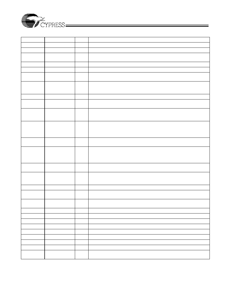
Note:
1.
These are the frequencies that are selectable after power up using the SEL1 and SEL0 hardware pins. Other frequencies may be chosen using the devices
SMBUS interface. See the expanded frequency for a complete listing of all of the availible frequencies.
2.
Will be set to 133MHz, when SMBUS Byte3, Bit 0 is set to logic 1.
Table 1. Function Table
[1]
TEST#
SEL1
SEL0
CPU(0:2)
SDRAM(0:5)
DCLK
3V66(0:2)
PCIF(1:6)
48M(0:1)
REF
IOAPIC(0:10)
0
X
0
Hi-Z
Hi-Z
Hi-Z
Hi-Z
Hi-Z
Hi-Z
Hi-Z
0
X
1
TCLK/2
TCLK/2
TCLK/3
TCLK/6
TCLK/2
TCLK
TCLK/6
1
0
0
66.6
100.0
[2]
66.6
33.3
48
14.318
33.3
1
0
1
100.0
100.0
[2]
66.6
33.3
48
14.318
33.3
1
1
0
133.3 133.3
66.6
33.3
48
14.318
33.3
1
1
1
133.3 100.0
[2]
66.6
33.3
48
14.318
33.3
Block Diagram
Pin Configuration
V D D C
V D D S
V D D
V D D P
V D D I
V D D
V D D S
P L L 1
R i n
i 2 c - c l k
i 2 c - d a t a
I O A P I C
t r i s t a t e
P D #
s 0
C P U
S D R A M
3 V 6 6
P C I
P L L 2
R i n
4 8
P D #
i 2 c - c l k
i 2 c - d a t a
3 6 p F
3 6 p F
3
6
3
6
2
2
1
1
V D D
X I N
X O U T
C P U ( 0 : 2 )
S D R A M ( 0 : 5 )
3 V 6 6 ( 0 : 2 )
P C I ( 1 : 6 )
I O A P I C ( 0 , 1 )
S D A T A
S C L K
P D #
S E L 0 , 1
T E S T #
4 8 M ( 0 , 1 )
D C L K
R E F
V C H _ C L K
C P U _ S T P #
P C I _ S T P #
1
V D D
V D D P
P C I _ F
1
2
3
4
5
6
7
8
9
10
11
12
13
14
15
16
17
18
19
20
21
22
23
24
29
30
31
32
33
34
35
36
37
38
39
40
41
42
43
44
45
46
47
48
XIN
V D D
S E L 1
XO U T
V S S
V S S
3V 6 6_0
3 V 66_ 1
3 V 66 _2(A G P )
P C I_F
P C I1
V S S
P C I3
V D D P
V D D
P C I2
P C I4
P C I5
V S S
A V D D
A V S S
V S S
T E S T #
C P U _S T P #
V D D
V C H _C L K
V D D S
S D R A M 5
D C LK
V S S
S D R A M 2
V D D S
S D R A M 0
V S S
C P U 2
C P U 1
S D R A M 4
S D R A M 3
S D R A M 1
V S S
V D D C
C P U 0
V D D I
IO A P IC 1
IO A P IC 0
V S S
P C I6
C
9
8
3
5
25
26
27
R E F
4 8M 0(U S B )
48 M 1(D O T )
28
V D D
S E L 0
S D A T A
S C LK
P D #
49
50
51
52
53
54
55
56
P C I_S T P #
C9835
Document #: 38-07303 Rev. **
Page 2 of 18
Note:
3.
A bypass capacitor (0.1
µ
F) should be placed as close as possible to each positive power pin. If these bypass capacitors are not close to the pins their
high-frequency filtering characteristic will be cancelled by the lead inductance of the traces.
Pin Description
[
3]
Pin
Name
PWR
Description
1
REF
VDD
3.3V 14.318 MHz clock output
3
XIN
VDD
Oscillator buffer input. Connect to a crystal or to an external clock.
4
XOUT
VDD
Oscillator buffer output. Connect to a crystal. Do not connect when an external
clock is applied at X
IN
.
49, 50, 52
CPU(0:2)
VDDC 2.5V Host bus clock outputs
7, 8, 9
3V66(0:2)
VDD
3.3V Fixed 66.6 MHz clock outputs
12
PCI_F
VDDP
3.3V PCI clock output. This clock continues to run when PCI_STP# is at a logic
low level.
13, 15, 16, 18,
19, 20
PCI (1:6)
VDDP
3.3V PCI clock outputs. These clocks synchronously stop in a low state when
PCI_STP# is brought to a logic low level. They synchronously resume running
when PCI_STP# is brought to a logic high state.
25, 26
48M(0,1)
VDD
3.3V Fixed 48 MHz clock outputs
36
VCH_CLK
VDD
3.3V selectable 66.6 MHz or 48 MHz clock output to VCH. Spread spectrum
applies only when 66.6 MHz is selected. Select via SMBUS, byte 4 bit7.
34
CPU_STP#
VDD
CPU0 stop clock control input. Stops only CPU0 in a low state when asserted
low. Using this pin to start and stop CPU0 clock insures synchronous (no short or
long clocks) transitioning of this clock.
11
PCI_STP#
VDD
PCI stop clock control input. When this signal is at a logic low level (0), all PCI
clocks (except PCI_F) stop at a logic low level. Using this pin to start and stop PCI
clocks insures synchronous (no short or long clocks) transitioning of these clocks.
This pin has no effect on the PCI_F clock.
28, 29
SEL(0,1)
VDD
3.3V LVTTL inputs for logic selection. These pins have Internal pull-ups,
typically 250k (range 200k to 800k).
30
SDATA
VDD
Serial data input pin. Conforms to the SMBUS specification of a Slave
Receive/Transmit device. This pin is an input when receiving data. It is an open
drain output when acknowledging or transmitting data. See 2-Wire SMBUS
Control Interface on page 7.
31
SCLK
VDD
Serial clock input pin. Conforms to the SMBUS specification. See 2-Wire
SMBUS Control Interface on page 7.
32
PD#
VDD
3.3V LVTTL-compatible input. When held LOW, the device enters a power down
mode. This pin has an Internal Pull-Up. See Power Management Functions on
page 3.
33
TEST#
VDD
3.3V LVTTL compatible input for selecting test mode. See Table 1.
38
DCLK
VDDS
3.3V SDRAM feedback clock output. See Table 1 for frequency selection. See
Figure 4 for timing relationship.
39, 40, 42, 43,
45, 46
SDRAM(0:5)
VDDS 3.3V SDRAM clock outputs
54, 55
IOAPIC(0,1)
VDDI
2.5V IOAPIC clock outputs. See Figure 4 for timing relationships.
37, 44
VDDS
3.3V Power for SDRAM and DCLK clock output buffers
17
VDDP
3.3V Power for PCI clock output buffers
53
VDDI
2.5V Power for IOAPIC clock output buffers
51
VDDC
2.5V Power for CPU clock output buffers
2, 10, 27, 35
VDD
3.3V Common power supply
22
AVDD
Analog power
23
AVSS
Analog ground
5, 6, 14, 21, 24,
41, 47, 48, 56
VSS
Common ground pins

C9835
Document #: 38-07303 Rev. **
Page 3 of 18
Power Management Functions
Power management on this device is controlled by the PD#,
CPU_STP# and PCI_STP# pins. When PD# is high (default)
the device is in normal running mode and all signals are active.
The PD# signal is used to bring all clocks to a low level in an
orderly fashion prior to power (all except AVDD) being
removed from the part. When PD# is asserted (forced) low, the
device transitions to a shutdown (power down) mode and all
power supplies (3.3V and 2.5V except for AVDD) may then be
removed. When PD# is sampled low by two consecutive rising
edges of the CPU clock, then all affected clocks are stopped
in a low state on their next high-to-low transition. The REF and
USB clocks are stopped in a low state as soon as possible.
When in power down (and before power is removed), all
outputs are synchronously stopped in a low state (see
Figure 1), all PLLs are shut off, and the crystal oscillator is
disabled. When the device is shutdown, the I≤C function is
also disabled.
At power-up, using the PD# select pin, all clocks are started in
such a manner as to guarantee a glitch-free operation, no
partial clock pulses.
Notes:
4.
Extended frequencies are only available via SMBUS interface. They are accessable via SMBUS Byte 5 bits 0,1.
5.
48M(0,1) clocks are constant at 48 MHz and REF is constant at 14.31818 MHz for all table selections.
6.
Will be set to 133 MHz and boosted accordingly, when Byte3,Bit 0 is set to logic 1.
Table 2. Expanded Frequency Selection (MHz)
[4, 5, 6]
TEST#
ESEL
ESEL
SEL
SEL
CPU(0:2)
SDRAM(0:5),
DCLK
3V66(0:2)
PCI_F,
PCI(1:6)
Notes
1
0
0
0
0
66.7
100
[6]
66.6
33
0% extension
(Default)
0
0
0
1
100
100
[6]
66.6
33
0
0
1
0
133.3
133.3
66.6
33
0
0
1
1
133.3
100
[6]
66.6
33
0
1
0
0
70
105
[6]
70
35
5% extension
0
1
0
1
105
105
[6]
70
35
0
1
1
0
140
140
70
35
0
1
1
1
140
105
[6]
70
35
1
0
0
0
73.3
110
[6]
73.3
36.6
10% extension
1
0
0
1
110
110
[6]
73.3
36.6
1
0
1
0
146.7
146.7
73.3
36.6
1
0
1
1
146.7
110
[6]
73.3
36.6
1
1
0
0
80
120
[6]
80
40
20% extension
1
1
0
1
120
120
[6]
80
40
1
1
1
0
160
160
80
40
1
1
1
1
160
120
[6]
80
40

C9835
Document #: 38-07303 Rev. **
Page 4 of 18
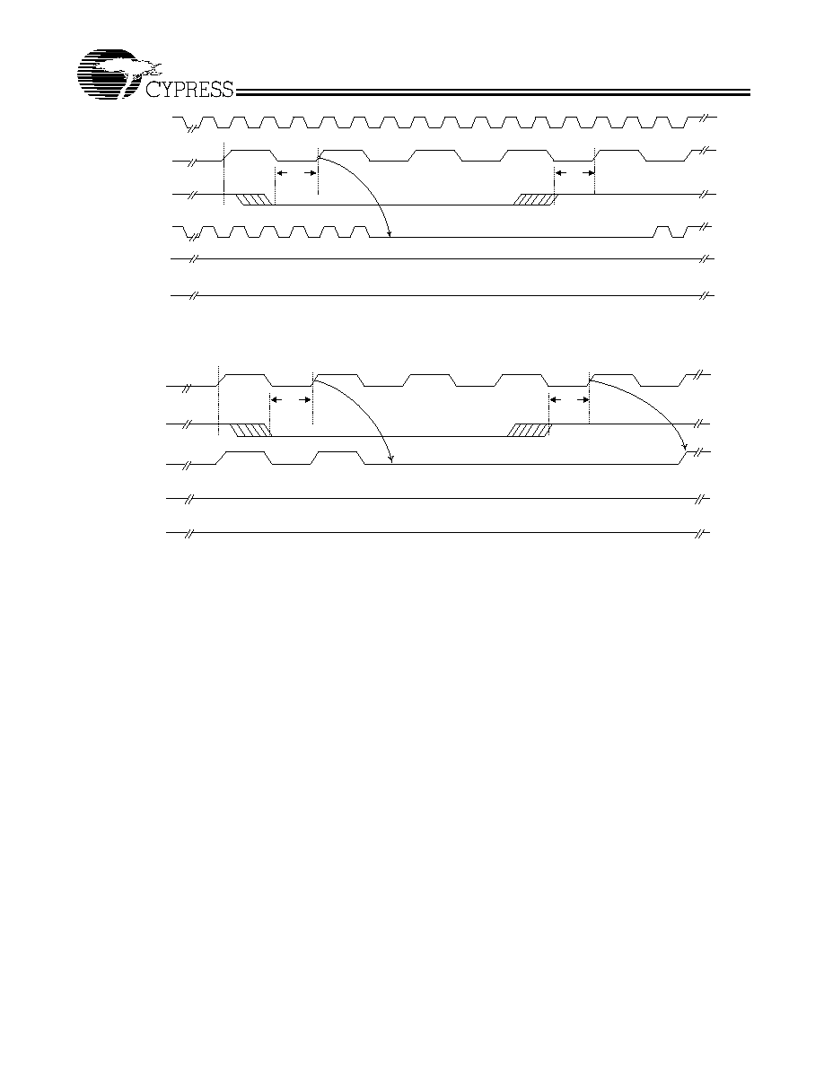
Power Management Timing
When exiting the power-down mode, the application must
supply power to the V
DD
pins a minimum of 200 ms before
releasing the PD# pin high to insure that an orderly startup will
occur and that the initial clocks that the device produces are
full and correctly compliant with data sheet specified phase
relationships.
CPU_STP# Timing
CPU_STP# is an input to the clock generator. CPU_STP# is
asserted asynchronously by the external clock control logic
and is internally synchronized to the external PCI_F output. All
other clocks will continue to run while the CPU0 clock is
disabled. The CPU0 is always stopped in a low state and
started in such a manner as to guarantee that the high pulse
width is a full pulse. Only one rising edge of PCI_F occurs after
the clock control logic is switched for the CPU0 output to
become enabled/disabled.
PCI_STP# Timing
PCI_STP# is an input to the clock generator and is made
synchronous to the clock driver PCI_F output. It is used to turn
off the PCI clocks for low power operation. PCI clocks are
stopped in a low state and started such that a full high pulse
width is guaranteed. ONLY one rising edge of PCI_F occurs
after the clock control logic switched for the PCI outputs to
become enabled/disabled.
Note:
7.
All internal timing is referenced to the CPU clock.
8.
CPU_STP# signal is an input signal that is made synchronous to free-running PCI_F.
9.
Diagrams shown with respect to 133 MHz. Similar operation when CPU is 100 MHz.
Table 3. Power Management Current
Conditions
Maximum 2.5V Current Consumption
(V
DDC
= V
DDI
= 2.625)
Maximum 3.3V Current Consumption
(V
DD
= AV
DD
= V
DDS
= 3.465V)
Power-down (PD# = LOW)
1
mA
1
mA
CPU = 66 MHz @ max loads
60 mA
295 mA
CPU = 100 MHz @ max loads
75 mA
295 mA
CPU = 133 MHz @ max loads
90 mA
295 mA
0ns
10ns
20ns
30ns
40ns
50ns
60ns
CPU 100 MHz
3V66 66 MHz
PCI 33 MHz
IOAPIC 33 MHz
PD#
SDRAM 100 MHz
REF 14.3 MHz
VCH_CLK , 48M (0,1)
Figure 1.
C9835
Document #: 38-07303 Rev. **
Page 5 of 18
Note:
10. All the internal timing is referenced to the CPU clock
11. PCI_STP# signal is an input signal that must be made synchronous to PCI_F output.
12. All other clocks continue to run undisturbed.
13. PD# is understood to in a high state.
14. Diagrams shown with respect to 133 MHz. Similar operation when CPU is 100 MHz
CPU(1,2)
PCI_F
CPU_STP#
CPU0
PCI_STP#
(High)
PWR_DWN#
Tsu
Tsu
(High)
Figure 2. CPU_STP Timing Diagram
PCI_STP#
PCI_F
(High)
(High)
PCI(1:6)
CPU_STP#
PD#
Tsu
Tsu
Figure 3. PCI_STP# Timing Diagram
[[10,11,12,13,14]